Note: Descriptions are shown in the official language in which they were submitted.
CA 02718339 2015-07-31
CARBON NANOTUBE-TRANSPARENT CONDUCTIVE INORGANIC
NANOPARTICLES HYBRID THIN FILMS FOR TRANSPARENT
CONDUCTIVE APPLICATIONS
COPYRIGHT NOTICE
[0001] This patent disclosure may contain material that is subject to
copyright
protection. The copyright owner has no objection to the facsimile reproduction
by
anyone of the patent document or the patent disclosure as it appears in the
U.S.
Patent and Tradcmark Office patent file or records, but otherwise reserves any
and
all copyright rights.
[0002] Deleted.
CROSS REFERENCE TO RELATED APPLICATIONS
[0003] This application claims thc benefit of U.S. Patent Application No.
61/036,755, filed on March 14, 2008
BACKGROUND OF THE INVENTION
[0004] The disclosed subject matter is in the field of transparent
conductive
coatings for display and touch screen applications.
[0005] Indium tin oxide (ITO) coatings on polyester films (like PET) are
commercially available and face a major technical hurdle in their
implementation
with flexible display applications due to the poor mechanical strength of the
ITO
film and its rapid mechanical failure on flexing.
[0006] On the other hand carbon nanotube (CNTs) based fihns have been
gaining importance in recent times as potential replacement for ITO in
transparent
conductive applications. Thc major advantage of carbon nanotubes is their
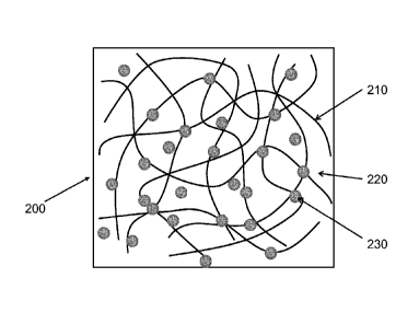
electrical
1
CA 02718339 2010-09-10
WO 2009/154830
PCT/US2009/037259
conductance, even in the form of a few nanometers thick film, coupled with
their
extreme mechanical flexibility. Since robust CNT films can be made at
extremely
small thicknesses, e.g., a CNT monolayer, the resulting films can be
transparent and
conductive. However, dense CNT networks cannot be made except with a loss in
the optical transparencies because CNTs are intrinsically light absorbing in
the
visible and UV regions.
[0007] Depositing a single dispersion of transparent conductive oxide
particles
with carbon nanotubes have been proposed. However, realization of such
methodology is thought to be extremely difficult due to flocculation of the
various
species during dispersion formation and/or during coating.
[0008] Laminates of transparent conductive oxide layers with carbon
nanotubes
layers have also been proposed. However, such structure nevertheless suffers
from
the respective problems associated with the single carbon nanotube (e.g., poor
optical transparencies) and single transparent conductive oxide films (e.g.,
poor
mechanical strengths) noted above.
SUMMARY
[0009] A carbon nanotube-transparent conductive inorganic nanoparticle
(CNT-
TCIN) hybrid film is provided that inherits the relative advantages of each of
the
individual components while overcoming the technical disadvantages of both the
films.
[0010] For example, while transparent conductive oxide (TCO) films
exhibit
poor mechanical strength, CNT-TCIN hybrid films exhibit excellent mechanical
strength. While TCO films exhibit a narrow electrical conductance range (e.g.,
films
having more than 5,000 ohms/square are non-uniform), CNT-TCIN hybrid films
exhibit wide range of electrical conductance (e.g., 1 ¨ 1010 ohms/square).
While
TCO films are not color neutral, CNT-TCIN hybrid films are color neutral.
While
TCO films are expensive and difficult to form because they are formed via
sputtering, CNT-TCIN hybrid films can be formed via simple, inexpensive
solution
deposition techniques. While TCO films exhibit poor RF absorption properties,
- 2 -
CA 02718339 2010-09-10
WO 2009/154830
PCT/US2009/037259
CNT-TCIN hybrid films exhibit good RF absorption properties and are useful in
military applications, antennas, and tags. While TCO films exhibit poor
environmental stability and many adhesion failures occur due to moisture and
temperature, CNT-TCIN hybrid films exhibit good stability at extreme moisture
and
temperatures without suffering adhesion failures. Lastly, while TCO films
exhibit
low charge carrier mobility (in the range of 1-100 cm2/(V s)), CNT-TCIN hybrid
films can exhibit high charge carrier mobility in optoelectronic devices and
transparent field effect transistors because the intrinsic hole mobility of
CNT films
can be as high as 105 cm2/(V s).
[0011] Moreover, while the visible light transmittance is acceptable for
only a
certain number of applications in CNT films, CNT-TCIN hybrid films exhibit
good
visible light transmittance for many applications. While infrared reflectance
is poor
for CNT films and excellent for TCO films, CNT-TCIN hybrid films can be tuned
for applications ranging from heat mirrors in buildings to optical modulators.
While
the surface roughness for CNT films typically cannot be decreased to a RMS
roughness of less than about 3.5 nm due to the bundling of the CNTs, CNT-TCIN
hybrid films can exhibit lower surface roughness.
[0012] The present invention further describes methods for forming a CNT-
TCIN hybrid film.
[0013] In one aspect, a conductive carbon nanotube layer includes a layer
of
carbon nanotubes deposited on a substrate to form a conductive and transparent
CNT network, hybridized by a population of TCINs distributed throughout the
network in an amount and at a location to provide a conductive transparent
layer.
[0014] In one or more embodiments, the layer further includes a coating
of
colloidal transparent conductive inorganic nanoparticles disposed on the upper
surface of the layer, said colloidal transparent conductive nanoparticles
having a
particle size less than the transparent conductive inorganic nanoparticles.
[0015] In another aspect, a method of preparing a composite carbon
nanotube
layer includes providing a first suspension of carbon nanotubes in a first
solvent;
providing a second suspension of transparent conductive inorganic
nanoparticles in a
second solution; applying the carbon nanotubes to a substrate to form a carbon
-3 -
CA 02718339 2010-09-10
WO 2009/154830
PCT/US2009/037259
nanotube network; and applying the colloidal transparent conductive inorganic
nanoparticles to the substrate to form a carbon nanotube network/transparent
conductive inorganic nanoparticles hybrid layer.
BRIEF DESCRIPTION OF THE DRAWINGS
[0016] The above and other objects and advantages of the present
invention will
be apparent upon consideration of the following detailed description, taken in
conjunction with the accompanying drawings, in which like reference characters
refer to like parts throughout, and in which:
[0017] Figure 1 is a schematic drawing of a monolayer of carbon
nanotubes, thin
bundles, deposited on a transparent substrate;
[0018] Figure 2 is a schematic cross sectional view of a monolayer of
carbon
nanotubes deposited on a transparent substrate;
[0019] Figure 3 is a schematic drawing of a monolayer of carbon nanotubes
deposited on a transparent substrate followed the deposition of transparent
conductive inorganic nanoparticle monolayer (TCIN);
[0020] Figure 4 is a schematic cross sectional view of a monolayer of
carbon
nanotubes deposited on a transparent substrate followed the deposition of
transparent conductive inorganic nanoparticle monolayer (TCIN);
[0021] Figure 5 is a schematic cross sectional view of carbon nanotubes-
TCIN
hybrid films formed on a transparent substratethrough multiple depositions;
[0022] Figure 6 is a schematic cross sectional view of a carbon nanotubes-
TCIN
hybrid film formed on a transparent substrate through multiple
depositionsfollowed
by deposition of a top most layer of transparent conductive oxide colloids
(TCOC)
in the size range of < 2 nm;
[0023] Figure 7 is a schematic representation of an assembly process in
accordance with certain embodiments of the present invention, where an
- 4 -
CA 02718339 2010-09-10
WO 2009/154830
PCT/US2009/037259
intermediate polyelectrolyte is used to bond CNT and ITO nanoparticles that
carry
the same charge and dispersed in their respective solvents;
[0024] Figure 8 is a schematic representation of an assembly process in
accordance with certain embodiments of the present invention, where no
intermediate polyelectrolyte is used to bond oppositely charged CNT and ITO
nanoparticles dispersed in their respective solvents;
[0025] Figure 9 shows the decrease of sheet resistance as a function of
successive coatings of the CNT film and a CNT-ITO hybrid film fabricated in
accordance with certain embodiments of the present invention;
[0026] Figure 10 is a comparison of sheet resistance and transmittance
for a
CNT film made from as produced carbon nanotubes and a CNT-ITO hybrid film
fabricated in accordance with certain embodiments of the present invention;
[0027] Figure 11 a shows Scanning Electron Micrograph (40,000X) of a CNT-
ITO hybrid film assembled in accordance with certain embodiments of the
present
invention;
[0028] Figure 12 shows a Scanning Electron Micrograph (60,000X) of a CNT-
ITO hybrid film assembled in accordance with certain embodiments of the
present
invention;
[0029] Figure 13 shows a comparison of the sheet resistance and
transmittance
for a CNT film and a CNT-ITO hybrid film made from purified carbon nanotubes
assembled in accordance with certain embodiments of the present invention; and
[0030] Figure 14 shows the photograph of a CNT ¨ITO hybrid film coated on
a
flexible PET substrate.
DETAILED DESCRIPTION OF THE INVENTION
[0031] The formation of carbon nanotube-transparent conductive oxide
hybrid
coatings on flexible plastic substrates, rigid plastic substrates and glass
substrates is
described.
[0032] Figure 1 is a schematic illustration of a monolayer of carbon
nanotubes,
thin bundles deposited on a transparent substrate and is illustrative of
conventional
conductive transparent CNT films. Figure 2 is a cross sectional view of the
same
CNT layer deposited on a transparent substrate. The thin film system 100
includes a
-5 -
CA 02718339 2010-09-10
WO 2009/154830
PCT/US2009/037259
transparent substrate layer 110 onto which a monolayer of carbon nanotubes 120
are
deposited. The layer can be very thin, for example, a CNT monolayer can be
about
1.35 nm thick.
STRUCTURE OF CNT-TCIN HYBRID FILMS
[0033] Flexible thin films of high conductivity and optical transmission
are
provided by introduction of TCINs into the CNT network. Figure 3 is a top view
and Figure 4 is a cross sectional view of a hybrid layer 200 including a
monolayer of
carbon nanotubes 210, as part of the hybrid, arranged in thin bundles,
deposited on a
transparent substrate 220. The hybrid layer further includes small transparent
conductive inorganic nanoparticles (TCINs) 230 that are distributed throughout
the
CNT monolayer 210. In one or more embodiments, the introduction of the TCINs
occurs after the deposition of the CNT monolayer. A single hybrid layer can
have a
thickness up to about 20 nm, and can be up to 10 nm in thickness and is for
example
about 2-5 nm thick.
[0034] Figure 5 is a schematic cross sectional view a CNT-TCIN hybrid
film
500 of increased thickness. The hybrid multilayers can range from moderately
thick
to very thin. For example, the films can have a thickness between about 5 nm
to
about 100 nm. In a preferred embodiment, the films can have a thickness
between
about 20 nm to about 25 nm.
[0035] As shown in Figures 3-5, the hybrid film contains a nanoscale
hybrid of
nanoparticles of transparent conductive oxides (TCO) (e.g., 2 nm ¨ 100 nm size
range) connected to each other through the network of carbon nanotubes.
[0036] The TCINs are located throughout the layer and may be in contact
with
one or more nanotubes. The size of the TCIN can be selected to be commensurate
with the thickness of the hybrid layer. For example, the TCINs have a particle
size
of up to about 20 nm, such as, about 2-5 nm.
[0037] In certain embodiments, the upper surface of the hybrid film can
further
be deposited with transparent conductive oxide colloids (TCOC) in the size
range of
1-2 nm. The TCOC may be prepared from In203:Sn, ZnO:F, Cd2Sn04, ZnO:Al,
5n02:F, ZnO:Ga, ZnO:B, 5n02:Sb, ZnO:In, and the like. In certain embodiments,
- 6 -
CA 02718339 2010-09-10
WO 2009/154830
PCT/US2009/037259
the TCOC may not form a continuous film across the upper portion of the hybrid
layer, but serve only to fill in certain regions that appear similar to voids
to
smoothen out the any surface roughness that may be present on the hybrid film.
In
certain embodiments, the mean thickness of the TCOC deposited on the upper
portion of the hybrid layer may be of a sufficient thickness so that the
mechanical
strength (brittleness) is at an acceptable range (e.g., 1-2 nm thick).
[0038] Figure 6 is a cross sectional view of the schematic of such a
structure
showing TCOC 600 in the size range of < 2 nm as the uppermost layer. The small
particle size of the TCOC permits the colloidal particles to penetrate into
the upper
portion of the hybrid layer and to form a smooth upper surface. Such layer of
TCOC
can be utilized to reduce the RMS surface roughness of the hybrid film. For
example, in OLED applications, it is desirable to have a surface roughness of
less
than 2 rms.
[0039] In one or more embodiments, instant films also have volume
resistances
in the range of about 10-2 ohms-cm to about 1010 ohms-cm. In other
embodiments,
the film has a surface resistance in the range of less than about 1010
ohms/square.
Preferably, the film has a surface resistance in the range of about 100-101
ohms/square. In other embodiments, the film has a surface resistance in the
range of
less than about 2000 or less than about 1000 ohms/square. For example, the
film
has a surface resistance in the range of about 10 to about 2000 ohms/square.
[0040] In one or more embodiments, devices including the hybrid layer
demonstrate excellent transparency and low haze. For example, the instant film
has
a total transmittance of at least about 60% or 70% (such as 75-95%) and a haze
value of visible light of about 2.0% or less. In some embodiments, the instant
films
have a haze value of 0.5% or less. Total light transmittance refers to the
percentage
of energy in the electromagnetic spectrum with wavelengths less than 1x10⁻² cm
that
passes through the films, thus necessarily including wavelengths of visible
light.
[0041] Without wishing to be bound by theory, such hybrid layer having
discrete
TCIN connected through a three-dimensional network of carbon nanotubes may
offer significant advantages over other morphologies, such as a multilayer
films
having a separate carbon nanotube layer and a separate TCO layer. For example,
the
- 7 -
CA 02718339 2010-09-10
WO 2009/154830
PCT/US2009/037259
TCINs can increase the conductivity of the layer due to their inherent
conductivity
and/or by creating an electrical shunt across high contact resistance CNT-CNT
junctions without causing any loss of optical transmission in the conductive
film.
[0042] In contrast, in a multilayered structure having distinct CNT
layers and
ITO layers, electric current would tend to flow through the least resistive
layer,
mostly ignoring the more resistive layer. Such effect would negate any
synergistic
advantages that may be obtained by the hybrid layer of the present invention.
Secondly, the ITO layer would suffer from the poor mechanical strength of
individual ITO films. The ITO layer could further develop cracks, defects, pin
holes, and the like and change the properties of the laminated stack in an
undesirable
way. Moreover, the optical and electrical properties of TCIN are heavily
dependent
on their mean particle size. Therefore, efforts to match the optical and
electrical
properties of the TCO layer with that of adjoining CNT layer poses a
significant
challenge because the resulting layer will inevitably have a different
optical/electrical properties from that of the starting TCIN.
SUITABLE MATERIALS FOR FORMING CNT-TCIN HYBRID FILMS
[0043] To make the hybrid transparent conductive films with one component
being carbon nanotubes, any conductive material having sufficient electrical
conductivity even at nanoscale dimensions and optical transparency may be
used.
By way of example, suitable TCINs include ITO, ZnO, Cd25n04, ZnSn03, among
others. Exemplary conductive metal oxides are listed below in Table 1.
Mixtures of
different TCINs may be used. In particular, the transparent conductive
inorganic
nanoparticle can be ITO.
- 8 -
CA 02718339 2010-09-10
WO 2009/154830
PCT/US2009/037259
Table 1. Metal oxides and their electrical and optical properties.
Material Sheet Resistance Visible Absorption
OM) Coefficient
In203:Sn 6 0.04
ZnO:F 5 0.03
Cd2SnO4 7.2 0.02
ZnO:Al 3.8 0.05
Sn02:F 8 0.04
ZnO: Ga 3 0.12
ZnO:B 8 0.06
Sn02:Sb 20 0.12
ZnO:In 20 0.20
Source: R.G.Gordon, MRS Bulletin, August 2000
[0044] The bulk resistivity of the transparent conductive oxides in their
nanoparticle form can be more than 3 orders larger than their bulk resistivity
in the
macroscopic solid or thin film form. The bulk resistivity range of the optical
transparent conductors may be in the range of 1-1000 gf2.cm and their plasma
wavelength can be as low as below 0.4 gm to more than > 1 gm.
[0045] The plasma frequency is the frequency above which the charge
carriers
do not respond to the electromagnetic radiation and the material behaves as a
transparent dielectric. Below the plasma frequencies, the TCO reflects and
absorbs
the incident radiation. For most transparent conductive materials, the plasma
frequency falls in the near-IR region of the electromagnetic radiation
(R.G.Gordan,
MRS Bulletin, Aug 2000).
[0046] In certain embodiments, TCINs diameters can range from few ten
nanometers to few microns. In other embodiments, the TCINs can be monodisperse
in size.
[0047] In some other embodiments, the TCINs can have any desirable
shapes,
such as spherical, oblong, prismatic, ellipsoidal, irregular objects, or in
the form of
nanorods. In the form of a nanorod the diameter of the rods can range from a
few
- 9 -
CA 02718339 2010-09-10
WO 2009/154830
PCT/US2009/037259
nanometers to several tens of nanometers. Their aspect ratio can be as low as
5 to
few thousand.
[0048] In certain embodiments, certain TCINs having an aspect ratio that
is
larger than 1 can lower the percolative conduction threshold for
interconnection of
the TCINs through a carbon nanotube network, thus improving optical
transparency
further.
[0049] The TCINs can be formed in the form of oxide sols by the
hydrolysis of
the corresponding metal-organic precursors. The mean diameter, size
dispersity, and
aspect ratios of the TCINs can be controlled by various factors like
concentrations,
temperature and duration of the reaction.
[0050] In certain embodiments, the interactions between CNT and TCIN can
be
tailored to exhibit certain attractive interactions with each other through
van der
Waals interactions, covalent interactions, electrostatic interactions, ionic
interactions, and/or any other suitable interactions.
[0051] For example, the CNTs and TCIN can be derivatized to carry
electrical
charges of specific polarity (e.g., positive or negative charges). For
example,
silylation of the surface of the TCINs with aminopropyl trimethoxy silane can
form
an amine terminated surface that is negatively charged. In contrast,
derivatizing the
TCIN with alkyl bromide terminal groups can render them positively charged.
[0052] In some other embodiments, TCINs can be functionalized with a
significant concentration of surface chemical species like hydroxyl groups
that can
then be used for the organic derivatization of the TCINs. The TCINs can be
modified further to impart other chemical functionalities, as would be readily
apparently to one of ordinary skill in the art. Some non-limiting examples of
chemical functionalities that may appear natively, or those that can be
prepared on
surfaces of the TCINs include ¨OH, -COOH, -NH2, ether, ester, amide, -C1, -Br,
and
the like functional groups
[0053] In some other embodiments, the surface chemistry of the
transparent
conductive oxide can be tailored to tether to the surface of the single walled
carbon
nanotubes through a covalent bonding.
[0054] In one or more embodiments, the nanotubes comprise single walled
carbon-based SWNT-containing material. SWNTs can be formed by a number of
- 10 -
CA 02718339 2015-07-31
techniques, such as laser ablation of a carbon target, combustion of
hydrocarbon
fuels, decomposing a hydrocarbon, and setting up an arc between two graphite
electrodes. For example, U.S. Pat. No. 5,985,232 to Howard et al. describes a
method for the production of nanotubes, in which unsaturated hydrocarbon fuel
and
oxygen are combusted in a burner chamber at a sub-atmospheric pressure,
thereby
establishing a flame. For example, U.S. Pat. No. 5,424,054 to Bethune et al.
describes a process for producing single-walled carbon nanotubes by contacting
carbon vapor with cobalt catalyst. The carbon vapor is produced by electric
arc
heating of solid carbon, which can be amorphous carbon, graphite, activated or
decolorizing carbon or mixtures thereof. Other techniques of carbon heating
are
contemplated, for instance laser heating, electron beam heating and RF
induction
heating. Smalley (Guo, T., Nikoleev, P., Thess, A., Colbert, D. T., and
Smally, R.
E., Chem. Phys. Lett. 243: 1-12 (1995)) describes a method of producing single-
walled carbon nanotubes wherein graphite rods and a transition metal are
simultaneously vaporized by a high-temperature laser. Smalley (Thess, A., Lee,
R.,
Nikolaev, P., Dai, H., Petit, P., Robert, J., Xu, C., Lee, Y. H., Kim, S. G.,
Rinzler, A.
G., Colbert, D. T., Scuseria, G. E., Tonarek, D., Fischer, J. E., and Smalley,
R. E.,
Science, 273: 483-487 (1996)) also describes a process for production of
single-
walled carbon nanotubes in which a graphite rod containing a small amount of
transition metal is laser vaporized in an oven at about 1200 C. Single-wall
nanotubes were reported to be produced in yields of more than 70%. U.S. Pat.
No.
6,221,330.
methods of producing single-walled carbon nanotubes which employs gaseous
carbon feedstocks and unsupported catalysts.
[0055] In certain embodiments, the CNT networks can be formed using long
nanotubes, such as nanotubes having a length longer than 1, 2, 3, 4, or 5
microns. In
other embodiments, the CNT networks can be formed using predominantly metallic
nanotubes or predominantly semiconducting nanotubes, or a mixture thereof. In
some other embodiments, the nanotubes can be selected so that the work
function
(i.e., the minimum energy required to remove an electron from the surface of a
particular material) of the nanotubes are matched with the work function of
the
TCINs.
- 11 -
CA 02718339 2010-09-10
WO 2009/154830
PCT/US2009/037259
[0056] Carbon nanotubes may also be obtained in the form of a dispersion
to
provide a CNT ink. Examples of such CNT dispersions are commercially available
from Brewer Science, Rolla, MO and Carbon Solutions, Inc., Riverside, CA among
others. Alternately the CNT dispersions can be tailor made by prior art
methods or
proprietary custom methods starting from raw carbon nanotubes.
[0057] The electronic structure of the single walled carbon nanotubes and
their
affinity to the coated substrate and the transparent conductive oxide
nanoparticles
can also be modified by chemical derivatization with one or more of organic
functional groups of similar or different types.
[0058] The substrate can be any conductive or non-conductive material,
for
example, metals, silicon, silicon oxide, plastics, organic polymers, inorganic
polymers, glasses, crystals, composite material, etc. The substrate for
example,
maybe, transparent, semi-transparent, translucent, or opaque.
METHODS FOR FORMING CNT-TCIN HYBRID FILMS
[0059] The CNT-TCIN hybrid films can be applied to a substrate from
suspension using any suitable solvent. The CNT-TCIN hybrid films can be formed
by an alternating deposition of CNT and TCINs from their respective
dispersions.
[0060] In certain embodiments, the CNT dispersion having from about 0.005
wt% to 1 wt% CNT in a suitable solvent can be utilized. In certain
embodiments,
TCIN dispersions having about 0.005wt% to 1 wt% TCIN in a suitable solvent can
be utilized. As would e readily apparent to one of ordinary skill in the art,
a suitable
dispersion/solution concentration may be utilized as would be readily apparent
to
one of ordinary skill in the art.
[0061] The number of depositions alternating between the CNT and TCINs
can
be controlled as desired. For example, the proportion of CNT:TCIN may range
from
about 10:90 to 90:10 by weight. When low amounts of CNTs are present, the film
may lose some of the flexibility and mechanical strength that are provided by
the
carbon nanotubes. When the amount of TCINs in the hybrid layer is low, the
conductivity enhancement of the material is compromised. Therefore, the
- 12 -
CA 02718339 2010-09-10
WO 2009/154830
PCT/US2009/037259
appropriate balance of materials is selected to provide the desired balance of
mechanical and electrical properties in the layer.
[0062] The number of layers and the density of each layer may be selected
to
obtain a target surface coverage. In one or more embodiments, the relative
surface
coverage of the CNTs and the TCINs can range from about 10:90 to 90:10, and in
some embodiments the surface coverage may be about 1:1. Total surface coverage
may range from about 10% to about 100%. A typical monolayer may provide up to
about 15% (of the CNT and TCIN combined) surface coverage.
[0063] If thicker layers are desired for lowering of the overall surface
resistance,
multiple hybrid layers can be applied to the substrate to achieve a thicker
hybrid film
(e.g., see Figure 5).
[0064] Additional binder materials can be utilized to assemble the
desired CNT-
TCIN structures. Figure 7 shows one embodiment to assemble the CNT-TCIN
hybrid film of the present invention. As shown therein, a transparent
substrate 700
can be pretreated with a binder material 710, such as a polymer, oligomer, a
small
organic molecule, a large organic molecule or a polyelectrolyte carrying one
particular charge (e.g., positively charged). After a rinse and dry cycle, the
substrate
having the binder can be immersed into a CNT solution 730 (step 720), where
the
CNTs may be charged oppositely to that of the binder material (e.g.,
negatively
charged). After a rinse and dry cycle, the CNT coated substrate can then be
immersed in the binder material 710 again (step 740), followed by another
rinse and
dry cycle. Thereafter, the coated substrate can be immersed in a TCIN solution
760
(step 750), where the TCINs may be charged oppositely to that of the binder
material (e.g., negatively charged, followed by a rinse and dry cycle. These
steps
can be repeated in a cyclic process as desired and as shown in Figure 7. Such
an
embodiment may be particularly useful when the CNTs and TCINs both carry same
electrical charge and the binder material carries an opposite charge.
[0065] In another embodiment, where CNT and TCINs carry opposite charges
in
their respective solutions, the CNT-TCIN hybrid film can be formed without the
use
of any binder materials, as exemplified in Figure 8. As shown therein, a
transparent
substrate 700 can be can be immersed into a CNT solution 800 , where the CNTs
may be charged positively or negatively. After a rinse and dry cycle, the CNT
coated
- 13 -
CA 02718339 2010-09-10
WO 2009/154830
PCT/US2009/037259
substrate can then be immersed in TCIN solution 810, where the TCINs are
charged
oppositely to that of the charge of the CNT in solution 800. After a rinse and
dry
cycle, these steps can be repeated in a cyclic process as desired and as shown
in
Figure 8.
[0066] As illustrated, numerous different embodiments are within the
scope of
one of ordinary skill in the art to form the CNT-TCIN hybrid film of the
present
invention.
[0067] Without wishing to be bound by theory, the hybrid layer thus
formed is
distinguished from a hybrid layer formed by depositing from a single
dispersion
because:
(a) the conditions required for forming stable dispersions of TCINs can
be distinct from conditions required for forming stable dispersions of CNT
(e.g.,
choice of solvent, pH, ionic strength, concentrations, etc.). The conditions
required
for each dispersion may be incompatible, leading to instant flocculation of
one or the
other species on standing; and
(b) the conditions for the application of a coating of transparent
conductive inorganic nanoparticles from a solution may be incompatible with
the
conditions required for application of a coating of CNT from a stable
dispersions
(e.g., surface treatment, temperature, flow stability, etc.). The incompatible
conditions may lead to flocculation of one or the other species during
coating.
[0068] Furthermore, without wishing to be bound by theory, the successive
deposition steps described in Figures 7 and 8 can be carried out under
suitable
conditions (e.g., at certain concentration of inks, deposition rate,
temperature,
viscosity,etc.) that advantageously form the morphology of the present
invention
(e.g., see Figures 3 and 4) rather than the multilayer films described in the
conventional art. For instance, by using charged TCINs, the TCIN can be made
to
repel each other and the low solution concentrations utilized can ensure
preventing
agglomeration of the TCINs to prevent formation of a continuous layer as in
the
conventional art. Such a technique of the present invention is distinguished
from the
various spray painting, spin coating, knife coating, ink jet printing and the
like
techniques that would generally form continuous films.
- 14 -
CA 02718339 2010-09-10
WO 2009/154830
PCT/US2009/037259
APPLICATIONS
[0069] The wavelength range for consideration of the optical properties
of the
CNT-TCIN hybrid films thus fabricated may be deep UV-UV (190-400nm), visible
(400-800nm), or infrared radiations 800-1800nm) or their combinations in
continuous or discrete segments. The CNT-TCIN hybrid films may have numerous
applications ranging from OLED, heat mirrors in buildings, optical modulators,
touchscreens, RF antennas, RF tags, and numerous other commercial and military
applications.
EXAMPLES
EXAMPLE 1: PREPARATION OF THE CNT INK FROM AS-PRODUCED CNT
[0070] The CNT ink consisting of negatively charged, unpurified carbon
nanotubes was prepared by adding 100 mg of as produced commercial single
walled
carbon nanotubes to a solution of 200 mg of polystyrene sulfonate in 100 ml of
deionized water. The mixture was sonicated for 12h in a bath sonicator. The
mixture
was left untouched for 48 hours and the supernatant liquid was decanted and
bottled.
EXAMPLE 2:PREPARATION OF CNT-INK FROM PURIFIED CNT
[0071] The CNT ink consisting of negatively charged, purified CNT, was
prepared by adding 50 mg of commercial single walled carbon nanotubes obtained
as purified to a solution of 200 mg of polystyrene sulfonate in 100 ml of
deionized
water. The mixture was sonicated for 12h in a bath sonicator. The mixture was
left
untouched for 48 hours and the supernatant liquid was decanted and bottled.
EXAMPLE 3: PREPARATION OF ITO-INK
[0072] The ITO ink consisting of negatively charged ITO nanoparticles was
prepared by adding 50 mg of as received commercial ITO nanoparticles having an
average size of 50 nm (Alfa-Aesar) to 100 ml of deionized water. The pH of the
solution was adjusted to 3 by the addition of hydrochloric acid. The mixture
was
sonicated in a bath sonicator for lh and it formed a shelf stable suspension.
The
mixture was used as such with no further centrifugation or decanting steps.
- 15 -
CA 02718339 2010-09-10
WO 2009/154830
PCT/US2009/037259
EXAMPLE 4: PREPARATION OF POLYMER ADHESIVE INK
[0073] The polymer ink, with a positively charged polymer to serve as a
binder
material between the CNT and ITO nanoparticles, was prepared by dissolving a
0.1% by weight portion of 2-hydroxy ethylcellulose (M.Wt 1,300,000) in
deionized
water.
EXAMPLE 5: PREPARATION OF 6-5 LAYER STACK USING CNT INK
FROM AS PRODUCED CNT.
[0074] The schematics of the layer by layer deposition of ITO and CNT is
shown in Figure 7. A precleaned glass substrate (700) was dipped in the
polymer
ink for two minutes, followed by rinsing in DI water, followed by dipping for
two
minutes in CNT ink (730), followed by rinsing in DI water. The substrate was
dried
with a gentle blow of air after each DI water rinse. Then, the coated
substrate was
dipped in the polymer ink again, followed by dipping for two minutes in the
ITO ink
(760) . The substrate again was rinsed with DI water and air-blow dried before
repeating the process all over as shown in Figure 7. The CNT-ITO hybrid film
was
obtained after such alternate addition of five layers each of CNT and ITO
respectively.
[0075] The sheet resistance and optical transparency of the samples were
measured as follows, after the addition of each layer of CNT, ITO and the
polymer.
[0076] The electrical resistance of the films were measured employing the
four
probe electrical equipment Lucas S-302-4 four point probe station with the 5P4-
40085TBY tip. The station was connected to an Agilent 3440A digital multimeter
for measuring resistance. The observed resistance values were multiplied by a
geometric correction factor of 4.53 to obtain the reported sheet resistances
expressed
in units of ohms/square. Optical properties of the transparent conductive
films were
measured employing a Agilent Technologies 8453 UV-Vis Chem Station
spectrophotometer. The reported transmittance values were observed at a
wavelength of 550nm.
- 16 -
CA 02718339 2010-09-10
WO 2009/154830
PCT/US2009/037259
[0077] The decrease in the sheet resistance with alternate addition of
CNT and
ITO coatings in the case of the hybrid film and that of a CNT-only control
film is
shown in Figure 9. The sheet resistance-transmittance data for the same set of
films
are shown in Figure 10. The continuous line represents the CNT-ITO hybrid film
and the dotted line represents the CNT-only film. In the case of the hybrid
film in
Figure 10, data points 1, 3, 5, 7 and 9 represent the CNT deposition and 2, 4,
6, 8,
and 10 represent the ITO deposition on top of the CNT network. Figures 9 and
10
demonstrate that a hybrid system is constructed through the electrical
"wiring" of
ITO nanoparticles by the conductive carbon nanotubes.
[0078] Control experiments conducted under identical conditions with a
film
made using only ITO nanoparticles ink (up to 8 coatings) and polymer ink
resulted
in an electrically non-conductive system (infinite sheet resistance) further
proving
the three dimensionally interconnected electrical "wiring" of ITO
nanoparticles by
CNT in the hybrid film.
[0079] The hybrid film was then annealed in an air oven at 300 C for 1
hour to
burn away the polymer. The polymer ink which was present as an extraneous
impurity is partially eliminated by thermal annealing resulting in a more
transparent
and less electrically resistive film represented by the data point 11 in the
case of the
CNT-ITO hybrid.
[0080] The control sample of containing only the ITO nanoparticles (up to
8
coatings) was also annealed and again showed infinite sheet resistance,
proving that
the polymeric binder material was not the cause of the observed electrical
property
in the control sample.
EXAMPLE 6: STRUCTURE AND MORPHOLOGY
[0081] The surface morphology of the CNT-ITO hybrid film, after the
annealing
step, was examined by scanning electron microscopy at different
magnifications,
employing an FEI Nova Nanolab dual beam FIB/SEM.
[0082] The scanning electron micrographs of the CNT-ITO hybrid film with
ITO as the top layer at 40,000x and 60,000x magnifications respectively are
shown
in Figures 11 and 12 respectively.
- 17 -
CA 02718339 2010-09-10
WO 2009/154830
PCT/US2009/037259
EXAMPLE 7: PREPARATION OF 6-5 LAYER STACK USING CNT INK
FROM PURIFIED CNT.
[0083] A precleaned glass substrate was dipped in the polymer iffl( for
two
minutes, followed by rinsing in DI water, followed by dipping for two minutes
in
CNT iffl( made from the purified CNT, and followed by rinsing in DI water. The
substrate was dried with a gentle blow of air after each DI water rinse. Then,
the
coated substrate was dipped in the polymer iffl( again, followed by dipping
for two
minutes in the ITO iffl(. The substrate again was rinsed with DI water and air-
blow
dried before repeating the process all over again until 7 coatings of purified
CNT ink
and 6 coatings of ITO ink were placed alternately. Electrical and transmission
measurements were made as described in the previous examples. The final hybrid
film showed a sheet resistance of less than 1000 ohms/square at an optical
transmittance of more than 0.85 as shown in Figure 13.
EXAMPLE 8: PREPARATION OF CNT-ITO HYBRID DEPOSITED ON A
FLEXIBLE PLASTIC SUBSTRATE.
[0084] A 3"x 1" sized polyethylene terephthalate (PET) substrate cut from
a
commercial film sample was dipped in the polymer ink for two minutes, followed
by rinsing in DI water, followed by dipping for two minutes in CNT ink (730),
followed by rinsing in DI water. The substrate was dried with a gentle blow of
air
after each DI water rinse. Then, the coated substrate was dipped in the
polymer ink
again, followed by dipping for two minutes in the ITO ink (760) . The
substrate
again was rinsed with DI water and air-blow dried. This process was repeated
until
a hybrid film with 9 coatings of CNT and 8 coatings of ITO were alternated to
form
the final sample. The sample exhibited an optical transmittance of 85% and
surface
resistance of 1500 ohms/square. A photograph of a portion of the hybrid film
cut
from the 3"xl" substrate is shown in Figure 14.
[0085] Upon review of the description and embodiments of the present
invention, those skilled in the art will understand that modifications and
equivalent
substitutions may be performed in carrying out the invention without departing
from
- 18 -
CA 02718339 2010-09-10
WO 2009/154830
PCT/US2009/037259
the essence of the invention. Thus, the invention is not meant to be limiting
by the
embodiments described explicitly above, and is limited only by the claims
which
follow.
What is claimed is:
- 19 -