Note: Descriptions are shown in the official language in which they were submitted.
CA 02718518 2010-09-15
WO 2009/117233 PCT/US2009/035486
INTERCONNECT ASSEMBLY
TECI-INICAL FIELD
[0001] Embodiments of the present invention relate generally to the field
of photovoltaic
technology.
BACKGROUND
[0002] In the drive for renewable sources of energy, photovoltaic
technology has assumed a
preeminent position as a cheap renewable source of clean energy. In
particular, solar cells based on
the compound semiconductor copper indium gallium diselenide (CIGS) used as an
absorber layer
offer great promise for thin-film solar cells having high efficiency and low
cost. Of comparable
importance to the technology used to fabricate thin-film solar cells
themselves, is the technology
used to collect current from the solar cells and to interconnect one solar
cell to another to form a
solar-cell module.
[0003] Just as the efficiency of thin-film solar cells is affected by
parasitic series resistances,
solar-cell modules fabricated from arrays of such thin-film solar cells are
also impacted by parasitic
series resistances. A significant challenge is the development of solar-cell,
current collection and
interconnection schemes that minimize the effects of such parasitic
resistances. Moreover, the
reliability of solar-cell modules based on such schemes is equally important
as it determines the
useful life of the solar-cell module and therefore its cost effectiveness and
viability as a reliable
alternative source of energy.
1
CA 02718518 2010-09-15
WO 2009/117233 PCT/US2009/035486
SUMMARY
[0004] Embodiments of the present invention include an interconnect
assembly. The
interconnect assembly includes a trace that includes a plurality of
electrically conductive portions.
The plurality of electrically conductive portions is configured both to
collect current from a first
solar cell and to interconnect electrically to a second solar cell. In
addition, the plurality of
electrically conductive portions is configured such that solar-cell efficiency
is substantially
undiminished in an event that any one of the plurality of electrically
conductive portions is
conductively impaired.
2
CA 02718518 2010-09-15
WO 2009/117233 PCT/US2009/035486
DESCRIPTION OF THE DRAWINGS
[0005] The accompanying drawings, which are incorporated in and form a part
of this
specification, illustrate embodiments of the invention and, together with the
description, serve to
explain the embodiments of the invention:
[0006] FIG. 1A is a cross-sectional elevation view of a layer structure of
a solar cell, in
accordance with an embodiment of the present invention.
[0007] FIG. 1B is a schematic diagram of a model circuit of a solar cell,
electrically
connected to a load, in accordance with an embodiment of the present
invention.
[0008] FIG. 2 is a schematic diagram of a model circuit of a solar-cell
module, electrically
connected to a load, that shows the interconnection of solar cells in the
solar-cell module, in
accordance with an embodiment of the present invention.
[0009] FIG. 3 is a schematic diagram of a model circuit of a solar-cell
module, electrically
connected to a load, that details model circuits of interconnect assemblies,
in accordance with an
embodiment of the present invention.
[0010] FIG. 4A is a schematic diagram of a model circuit of an interconnect
assembly for
connecting two solar cells of a solar-cell module, in accordance with an
embodiment of the present
invention.
[0011] FIG. 4B is a plan view of the interconnect assembly of FIG. 4A that
shows the
physical interconnection of two solar cells in the solar-cell module, in
accordance with an
embodiment of the present invention.
[0012] FIG. 4C is a cross-sectional, elevation view of the interconnect
assembly of FIG. 4B
that shows the physical interconnection of two solar cells in the solar-cell
module, in accordance
with an embodiment of the present invention.
[0013] FIG. 4D is a cross-sectional, elevation view of an alternative
interconnect assembly
for FIG. 4B that shows an edge-conforming interconnect assembly for the
physical interconnection
3
CA 02718518 2010-09-15
WO 2009/117233 PCT/US2009/035486
of two solar cells in the solar-cell module, in accordance with an embodiment
of the present
invention.
[0014] FIG. 4E is a cross-sectional, elevation view of an alternative
interconnect assembly
for FIG. 4B that shows a shingled-solar-cell arrangement for the physical
interconnection of two
solar cells in the solar-cell module, in accordance with an embodiment of the
present invention.
[0015] FIG. 4F is a plan view of an alternative interconnect assembly for
FIG. 4A that shows
the physical interconnection of two solar cells in the solar-cell module, in
accordance with an
embodiment of the present invention.
[0016] FIG. 5A is a plan view of the combined applicable carrier film,
interconnect assembly
that shows the physical arrangement of a trace with respect to a top carrier
film and a bottom carrier
film in the combined applicable carrier film, interconnect assembly, in
accordance with an
embodiment of the present invention.
[0017] FIG. 5B is a cross-sectional, elevation view of the combined
applicable carrier film,
interconnect assembly of FIG. 5A that shows the physical arrangement of a
trace with respect to a
top carrier film in the combined applicable carrier film, interconnect
assembly prior to disposition
on a solar cell, in accordance with an embodiment of the present invention.
[0018] FIG. 5C is a cross-sectional, elevation view of the interconnect
assembly of FIG. 5B
that shows the physical arrangement of a trace with respect to a top carrier
film in the combined
applicable carrier film, interconnect assembly after disposition on a solar
cell, in accordance with an
embodiment of the present invention.
[0019] FIG. 6A is a plan view of an integrated busbar-solar-cell-current
collector that shows
the physical interconnection of a terminating solar cell with a terminating
busbar in the integrated
busbar-solar-cell-current collector, in accordance with an embodiment of the
present invention.
[0020] FIG. 6B is a cross-sectional, elevation view of the integrated
busbar-solar-cell-current
collector of FIG. 6A that shows the physical interconnection of the
terminating solar cell with the
4
CA 02718518 2010-09-15
WO 2009/117233 PCT/US2009/035486
terminating busbar in the integrated busbar-solar-cell-current collector, in
accordance with an
embodiment of the present invention.
[0021] FIG. 7A is a combined cross-sectional elevation and perspective view
of a roll-to-roll,
interconnect-assembly fabricator for fabricating the interconnect assembly
from a first roll of top
carrier film and from a dispenser of conductive-trace material, in accordance
with an embodiment of
the present invention.
[0022] FIG. 7B is a combined cross-sectional elevation and perspective view
of a roll-to-roll,
laminated-interconnect-assembly for fabricating a laminated-interconnect
assembly from the first
roll of top carrier film, from a second roll of bottom carrier film and from
the dispenser of
conductive-trace material, in accordance with an embodiment of the present
invention.
[0023] FIG. 8 is flow chart illustrating a method for roll-to-roll
fabrication of an interconnect
assembly, in accordance with an embodiment of the present invention.
[0024] FIG. 9 is flow chart illustrating a method for interconnecting two
solar cells, in
accordance with an embodiment of the present invention.
[0025] The drawings referred to in this description should not be
understood as being drawn
to scale except if specifically noted.
CA 02718518 2016-06-10
DESCRIPTION OF EMBODIMENTS
[0026] Reference will now be made in detail to the various embodiments of
the present
invention. While the invention will be described in conjunction with the
various embodiments, it
will be understood that they are not intended to limit the invention to these
embodiments.
[0027] Furthermore, in the following description of embodiments of the
present invention,
numerous specific details are set forth in order to provide a thorough
understanding of the present
invention. However, it should be appreciated that embodiments of the present
invention may be
practiced without these specific details. In other instances, well known
methods, procedures, and
components have not been described in detail as not to unnecessarily obscure
embodiments of the
present invention.
=
PHYSICAL DESCRIPTION OF EMBODIMENTS OF THE PRESENT INVENTION FOR AN
INTERCONNECT
ASSEMBLY
[0028] With reference to FIG. 1A, in accordance with an embodiment of the
present
invention, a cross-sectional elevation view of a layer structure of a solar
cell 100A is shown. The
solar cell 100A includes a metallic substrate 104. In accordance with an
embodiment of the present
invention, an absorber layer 112 is disposed on the metallic substrate 104;
the absorber layer 112
may include a layer of the material copper indium gallium diselenide (CIGS)
having the chemical
formula Cu(In1.xGax)Se2, where x may be a decimal less than one but greater
than zero that
determines the relative amounts of the constituents, indium, In, and gallium,
Ga. Alternatively,
semiconductors having the chalcopyrite crystal structure, for example,
chemically homologous
compounds with the compound CIGS having the chalcopyrite crystal structure, in
which alternative
elemental constituents are substituted for Cu, In, Ga, and/or Se, may be used
as the absorber layer
6
CA 02718518 2016-06-10
112. Moreover, in embodiments of the present invention, it should be noted
that semiconductors,
such as silicon and cadmium telluride, as well as other semiconductors, may be
used as the absorber
layer 112.
[0029] As shown, the absorber layer 112 includes a p-type portion 112a and
an n-type portion
112b. As a result, a pn homojunction 112c is produced in the absorber layer
112 that serves to
separate charge carriers that are created by light incident on the absorber
layer 112. To facilitate the
efficient conversion of light energy to charge carriers in the absorber layer
112, the composition of
the p-type portion 112a of the absorber layer 112 may vary with depth to
produce a graded band gap
of the absorber layer 112. Alternatively, the absorber layer 112 may include
only a p-type
chalcopyrite semiconductor layer, such as a CIGS material layer, and a pn
heterojunction may be
produced between the absorber layer 112 and an n-type layer, such as a metal
oxide, metal sulfide or
metal selenide, disposed on its top surface in place of the n-type portion
112b shown in FIG. 1A.
However, embodiments of the present invention are not limited to pn junctions
fabricated in the
manner described above, and could also include a generic pn junction produced
either as a
homojunction in a single semiconductor material, or alternatively a
heterojunction between two
different semiconductor materials. Moreover, in embodiments of the present
invention, it should be
noted that semiconductors, such as silicon and cadmium telluride, as well as
other semiconductors,
may be used as the absorber layer 112.
10030] In accordance with an embodiment of the present invention, on the
surface of the n-
type portion 112b of the absorber layer 112, one or more transparent
electrically conductive oxide
(TCO) layers 116 are disposed, for example, to provide a means for collection
of current from the
absorber layer 112 for conduction to an external load. As used herein, it
should be noted that the
phrase "collection of current" refers to collecting current carriers of either
sign, whether they be
positively charged holes or negatively charged electrons; for the structure
shown in FIG. IA in
7
CA 02718518 2010-09-15
WO 2009/117233 PCT/US2009/035486
which the TCO layer is disposed on the n-type portion 112b, the current
carriers collected under
normal operating conditions are negatively charged electrons; but, embodiments
of the present
invention apply, without limitation thereto, to solar cell configurations
where a p-type layer is
disposed on an n-type absorber layer, in which case the current carriers
collected may be positively
charged holes. The TCO layer 116 may include zinc oxide, ZnO, or alternatively
a doped
conductive oxide, such as aluminum zinc oxide (AZO), AlxZn1_x0y, and indium
tin oxide (ITO),
InxSn1_x0y, where the subscripts x and y indicate that the relative amount of
the constituents may be
varied. Alternatively, the TCO layer 116 may be composed of a plurality of
conductive oxide layers.
These TCO layer materials may be sputtered directly from an oxide target, or
alternatively the TCO
layer may be reactively sputtered in an oxygen atmosphere from a metallic
target, such as zinc, Zn,
Al-Zn alloy, or In-Sn alloy targets. For example, the zinc oxide may be
deposited on the absorber
layer 112 by sputtering from a zinc-oxide-containing target; alternatively,
the zinc oxide may be
deposited from a zinc-containing target in a reactive oxygen atmosphere in a
reactive-sputtering
process. The reactive-sputtering process may provide a means for doping the
absorber layer 112
with an n-type dopant, such as zinc, Zn, or indium, In, to create a thin n-
type portion 112b, if the
partial pressure of oxygen is initially reduced during the initial stages of
sputtering a metallic target,
such as zinc, Zn, or indium, In, and the layer structure of the solar cell
100A is subsequently
annealed to allow interdiffusion of the zinc, Zn, or indium, In, with CIGS
material used as the
absorber layer 112. Alternatively, sputtering a compound target, such as a
metal oxide, metal sulfide
or metal selenide, may also be used to provide the n-type layer, as described
above, on the p-type
portion 112a of the absorber layer 112.
[0031] With further reference to FIG. 1A, in accordance with the embodiment
of the present
invention, a conductive backing layer 108 may be disposed between the absorber
layer 112 and the
metallic substrate 104 to provide a diffusion barrier between the absorber
layer 112 and the metallic
substrate 104. The conductive backing layer 108 may include molybdenum, Mo, or
other suitable
8
CA 02718518 2016-06-10
metallic layer having a low propensity for interdiffusion with an absorber
layer 112, such as one
composed of CIGS material, as well as a low diffusion coefficient for
constituents of the substrate.
Moreover, the conductive backing layer 108 may provide other functions in
addition to, or
independent of, the diffusion-barrier function, for example, a light-
reflecting function, for example,
as a light-reflecting layer, to enhance the efficiency of the solar cell, as
well as other functions. The
embodiments recited above for the conductive backing layer 108 should not be
construed as limiting
the function of the conductive backing layer 108 to only those recited.
[0032] With reference now to FIG. 1B, in accordance with an embodiment of
the present
invention, a schematic diagram of a model circuit 100B of a solar cell that is
electrically connected
to a load is shown. The model circuit 100B of the solar cell includes a
current source 158 that
generates a photocurrent, L. As shown in FIG. 1A, the current source 158 is
such as to produce
counterclockwise electrical current, or equivalently an clockwise electron-
flow, flowing around
each of the loops of the circuit shown; embodiments of the present invention
also apply, without
limitation thereto, to solar-cell circuits in which the electrical current
flows in a clockwise direction,
or equivalently electrons flow in a counterclockwise direction. The
photocurrent, iL, is produced
when a plurality of incident photons, light particles, of which one example
photon 154 with energy,
by, is shown, produce electron-hole pairs in the absorber layer 112 and these
electron-hole pairs are
separated by the pn homojunction 112c, or in the alternative, by a pn heteroj
unction as described
above. It should be appreciated that the energy, hv, of each incident photon
of the plurality of
photons should exceed the band-gap energy, Eg, that separates the valence band
from the conduction
band of the absorber layer 112 to produce such electron-hole pairs, which
result in the photocurrent,
9
CA 02718518 2010-09-15
WO 2009/117233 PCT/US2009/035486
[0033] The model circuit 100B of the solar cell further includes a diode
162, which
corresponds to recombination currents, primarily at the pn homojunction 112c,
that are shunted
away from the connected load. As shown in FIG. 1B, the diode is shown having a
polarity
consistent with electrical current flowing counterclockwise, or equivalently
electron-flow
clockwise, around the loops of the circuit shown; embodiments of the present
invention apply,
without limitation thereto, to a solar cell in which the diode of the model
circuit has the opposite
polarity in which electrical current flows clockwise, or equivalently electron-
flow flows
counterclockwise, around the loops of the circuit shown. In addition, the
model circuit 100B of the
solar cell includes two parasitic resistances corresponding to a shunt
resistor 166 with shunt
resistance, Rsh, and to a series resistor 170 with series resistance, Rs. The
solar cell may be
connected to a load represented by a load resistor 180 with load resistance,
RL. Thus, the circuit
elements of the solar cell include the current source 158, the diode 162 and
the shunt resistor 166
connected across the current source 158, and the series resistor 170 connected
in series with the load
resistor 180 across the current source 158, as shown. As the shunt resistor
166, like the diode 162,
are connected across the current source 158, these two circuit elements are
associated with internal
electrical currents within the solar cell shunted away from useful application
to the load. As the
series resistor 170 connected in series with the load resistor 180 are
connected across the current
source 158, the series resistor 170 is associated with internal resistance of
the solar cell that limits
the electrical current to the load.
[0034] With further reference to FIG. 1B, it should be recognized that the
shunt resistance
may be associated with surface leakage currents that follow paths at free
surfaces that cross the pn
homojunction 112c; free surfaces are usually found at the edges of the solar
cell along the side walls
of the device that define its lateral dimensions; such free surfaces may also
be found at
discontinuities in the absorber layer 112 that extend past the pn homojunction
112c. The shunt
resistance may also be associated with shunt defects which may be present that
shunt electrical
CA 02718518 2010-09-15
WO 2009/117233 PCT/US2009/035486
current away from the load. A small value of the shunt resistance, Rsh, is
undesirable as it lowers the
open circuit voltage, Voc, of the solar cell, which directly affects the
efficiency of the solar cell.
Moreover, it should also be recognized that the series resistance, Rs, is
associated with: the contact
resistance between the p-type portion 112a and the conductive backing layer
108, the bulk
resistance of the p-type portion 112a, the bulk resistance of the n-type
portion 112b, the contact
resistance between the n-type portion 112b and TCO layer 116, and other
components, such as
conductive leads, and connections in series with the load. These latter
sources of series resistance,
conductive leads, and connections in series with the load, are germane to
embodiments of the
present invention as interconnect assemblies, which is subsequently described.
A large value of the
series resistance, Rs, is undesirable as it lowers the short circuit current,
Isc, of the solar cell, which
also directly affects the efficiency of the solar cell.
[0035] With reference now to FIG. 2, in accordance with an embodiment of
the present
invention, a schematic diagram of a model circuit 200 of a solar-cell module
204 that is coupled to a
load is shown. The load is represented by a load resistor 208 with load
resistance, RL, as shown. The
solar-cell module 204 of the model circuit 200 includes a plurality of solar
cells: a first solar cell
210 including a current source 210a that generates a photocurrent, iu,
produced by example photon
214 with energy, hvi, a diode 210b and a shunt resistor 210c with shunt
resistance, Rshi; a second
solar cell 230 including a current source 230a that generates a photocurrent,
iL2, produced by
example photon 234 with energy, hv2, a diode 230b and a shunt resistor 230c
with shunt resistance,
Rsh2; and, a terminating solar cell 260 including a current source 260a that
generates a photocurrent,
iL3, produced by example photon 264 with energy, hvõ, a diode 260b and a shunt
resistor 260c with
shunt resistance, Rshõ. Parasitic series internal resistances of the
respective solar cells 210, 230 and
260 have been omitted from the schematic diagram to simplify the discussion.
Instead, series
resistors with series resistances, RSI5 Rs2 and Rsõ are shown disposed in the
solar-cell module 204 of
11
CA 02718518 2010-09-15
WO 2009/117233 PCT/US2009/035486
the model circuit 200 connected in series with the solar cells 210, 230 and
260 and the load resistor
208.
[0036] As shown in FIGS. 2 and 3, the current sources are such as to
produce
counterclockwise electrical current, or equivalently an clockwise electron-
flow, flowing around
each of the loops of the circuit shown; embodiments of the present invention
also apply, without
limitation thereto, to solar-cell circuits in which the electrical current
flows in a clockwise direction,
or equivalently electrons flow in a counterclockwise direction. Similarly, as
shown in FIGS. 2 and
3, the diode is shown having a polarity consistent with electrical current
flowing counterclockwise,
or equivalently electron-flow clockwise, around the loops of the circuit
shown; embodiments of the
present invention apply, without limitation thereto, to a solar cell in which
the diode of the model
circuit has the opposite polarity in which electrical current flows clockwise,
or equivalently
electron-flow flows counterclockwise, around the loops of the circuit shown.
[0037] With further reference to FIG. 2, in accordance with an embodiment
of the present
invention, the series resistors with series resistances R51 and Rs2 correspond
to interconnect
assemblies 220 and 240, respectively. Series resistor with series resistance,
R51, corresponding to
interconnect assembly 220 is shown configured both to collect current from the
first solar cell 210
and to interconnect electrically to the second solar cell 230. Series resistor
with series resistance,
Rsn, corresponds to an integrated solar-cell, current collector 270. The
ellipsis 250 indicates
additional solar cells and interconnect assemblies (not shown) coupled in
alternating pairs in series
in model circuit 200 that make up the solar-cell module 204. Also, in series
with the solar cells 210,
230 and 260 are a first busbar 284 and a terminating busbar 280 with series
resistances RBI and RB2,
respectively, that carry the electrical current generated by solar-cell module
204 to the load resistor
208. The series resistor with resistance Rs,, corresponding to the integrated
solar-cell, current
collector 270, and RB2, corresponding to the terminating busbar 280, in
combination correspond to a
integrated busbar-solar-cell-current collector 290 coupling the terminating
solar cell 260 with the
12
CA 02718518 2010-09-15
WO 2009/117233 PCT/US2009/035486
load resistor 208. In addition, series resistor with resistance Rs1,
corresponding to interconnect
assembly 220, and first solar cell 210 in combination correspond to a combined
solar-cell,
interconnect assembly 294.
[0038] As shown in FIG. 2 and as used herein, it should be noted that the
phrases "to collect
current," "collecting current" and "current collector" refer to collecting,
transferring, and/or
transmitting current carriers of either sign, whether they be positively
charged holes or negatively
charged electrons; for the structures shown in FIGS. 1A-B, 2, 3, 4A-F, 5A-C
and 6A-B, in which
an interconnect assembly is disposed above and electrically coupled to an n-
type portion of the solar
cell, the current carriers collected under normal operating conditions are
negatively charged
electrons. Moreover, embodiments of the present invention apply, without
limitation thereto, to
solar cell configurations where a p-type layer is disposed on an n-type
absorber layer, in which case
the current carriers collected may be positively charged holes, as would be
the case for solar cells
modeled by diodes and current sources of opposite polarity to those of FIGS.
1A-B, 2, 3, 4A-F, 5A-
C and 6A-B. Therefore, in accordance with embodiments of the present
invention, a current
collector and associated interconnect assembly that collects current may,
without limitation thereto,
collect, transfer, and/or transmit charges associated with an electrical
current, and/or charges
associated with an electron-flow, as for either polarity of the diodes and
current sources described
herein, and thus for either configuration of a solar cell with an n-type layer
disposed on and
electrically coupled to a p-type absorber layer or a p-type layer disposed on
and electrically coupled
to an n-type absorber layer, as well as other solar cell configurations.
[0039] With further reference to FIG. 2, in accordance with an embodiment
of the present
invention, the series resistances of the interconnect assemblies 220 and 240,
integrated solar-cell,
current collector 270, and the interconnect assemblies included in ellipsis
250 can have a substantial
net series resistance in the model circuit 200 of the solar-cell module 204,
unless the series
resistances of the interconnect assemblies 220 and 240, integrated solar-cell,
current collector 270,
13
CA 02718518 2010-09-15
WO 2009/117233 PCT/US2009/035486
and the interconnect assemblies included in ellipsis 250 are made small. If a
large plurality of solar
cells are connected in series, the short circuit current of the solar-cell
module, Iscm, may be reduced,
which also directly affects the solar-cell-module efficiency analogous to the
manner in which solar-
cell efficiency is reduced by a parasitic series resistance, Rs, as described
above with reference to
FIG. 1. Embodiments of the present invention provide for diminishing the
series resistances of the
interconnect assemblies 220 and 240, integrated solar-cell, current collector
270, and the
interconnect assemblies included in ellipsis 250.
[0040] With reference now to FIG. 3, in accordance with embodiments of the
present
invention, a schematic diagram of a model circuit 300 of a solar-cell module
304 is shown that
illustrates embodiments of the present invention such that the series
resistances of the interconnect
assemblies 320 and 340, integrated solar-cell, current collector 370, and the
interconnect assemblies
included in ellipsis 350 are made small. The solar-cell module 304 is coupled
to a load represented
by a load resistor 308 with load resistance, RL, as shown. The solar-cell
module 304 of the model
circuit 300 includes a plurality of solar cells: a first solar cell 310
including a current source 310a
that generates a photocurrent, 1L1, produced by example photon 314 with
energy, hvi, a diode 310b
and a shunt resistor 310c with shunt resistance, RAI; a second solar cell 330
including a current
source 330a that generates a photocurrent, iL2, produced by example photon 334
with energy, hv2, a
diode 330b and a shunt resistor 330c with shunt resistance, R51Q; and, a
terminating solar cell 360
including a current source 360a that generates a photocurrent, 1L3, produced
by example photon 364
with energy, hvn, a diode 360b and a shunt resistor 360c with shunt
resistance, Rim.
[0041] With further reference to FIG. 3, in accordance with an embodiment
of the present
invention, the interconnect assemblies 320 and 340 and the integrated solar-
cell, current collector
370, with respective equivalent series resistances R51, R52 and R511 are shown
disposed in the solar-
cell module 304 of the model circuit 300 connected in series with the solar
cells 310, 330 and 360
14
CA 02718518 2010-09-15
WO 2009/117233 PCT/US2009/035486
and the load resistor 308. The ellipsis 350 indicates additional solar cells
and interconnect
assemblies (not shown) coupled in alternating pairs in series in model circuit
300 that make up the
solar-cell module 304. Also, in series with the solar cells 310, 330 and 360
are a first busbar 384
and a terminating busbar 380 with series resistances RBI and RB2,
respectively, that carry the
electrical current generated by solar-cell module 304 to the load resistor
308. The integrated solar-
cell, current collector 370 with resistance Rsõ, and the series resistor with
series resistance RB2,
corresponding to the terminating busbar 380, in combination correspond to an
integrated busbar-
solar-cell-current collector 390 coupling the terminating solar cell 360 with
the load resistor 308. In
addition, interconnect assembly 320 with resistance, Rs2, and solar cell 310
in combination
correspond to a combined solar-cell, interconnect assembly 394.
[0042] With further reference to FIG. 3, in accordance with embodiments of
the present
invention, the interconnect assembly 320 includes a trace including a
plurality of electrically
conductive portions, identified with resistors 320a, 320b, 320c, and 320m with
respective
resistances, rpli, rpi2, rp13 and rpim, and the ellipsis 320i indicating
additional resistors (not shown). It
should be noted that although the plurality of electrically conductive
portions of the trace are
modeled here as discrete resistors the interconnection with solar cell 330 is
considerably more
complicated involving the distributed resistance in the TCO layer of the solar
cell, which has been
omitted for the sake of elucidating functional features of embodiments of the
present invention.
Therefore, it should be understood that embodiments of the present invention
may also include,
without limitation thereto, the effects of such distributed resistances on the
trace. The plurality of
electrically conductive portions, without limitation thereto, identified with
resistors 320a, 320b,
320c, 320i, and 320m, are configured both to collect current from the first
solar cell 310 and to
interconnect electrically to the second solar cell 330. The plurality of
electrically conductive
portions, identified with resistors 320a, 320b, 320c, 320i, and 320m, are
configured such that upon
interconnecting the first solar cell 310 and the second solar cell 330 the
plurality of electrically
CA 02718518 2010-09-15
WO 2009/117233 PCT/US2009/035486
conductive portions are connected electrically in parallel between the first
solar cell 310 and the
second solar cell 330.
[0043] Thus, in accordance with embodiments of the present invention, the
plurality of
electrically conductive portions is configured such that equivalent series
resistance, Rs1, of the
interconnect assembly 320 including the parallel network of resistors 320a,
320b, 320c, 320i, and
320m, is less than the resistance of any one resistor in the parallel network.
Therefore, upon
interconnecting the first solar cell 310 with the second solar cell 330, the
equivalent series
resistance, R51, of the interconnect assembly 320, is given approximately,
omitting the effects of
distributed resistances at the interconnects with the first and second solar
cells 310 and 330, by the
formula for a plurality of resistors connected electrically in parallel, viz.
R51 = 1/[E(1/rp1i)], where
rpii is the resistance of the ith resistor in the parallel-resistor network,
and the sum, E, is taken over
all of the resistors in the network from i =1 torn. Hence, by connecting the
first solar cell 310 to the
second solar cell 330, with the interconnect assembly 320, the series
resistance, Rs1, of the
interconnect assembly 320 can be reduced lowering the effective series
resistance between solar
cells in the solar-cell module 304 improving the solar-cell-module efficiency.
[0044] Moreover, in accordance with embodiments of the present invention,
the
configuration of the plurality of electrically conductive portions due to this
parallel arrangement of
electrically conductive portions between the first solar cell 310 and the
second solar cell 330
provides a redundancy of electrical current carrying capacity between
interconnected solar cells
should one of the plurality of electrically conductive portions become
damaged, or its reliability
become impaired. Thus, embodiments of the present invention provide that the
plurality of
electrically conductive portions is configured such that solar-cell efficiency
is substantially
undiminished in an event that any one of the plurality of electrically
conductive portions is
conductively impaired, because the loss of electrical current through any one
electrically conductive
16
CA 02718518 2010-09-15
WO 2009/117233 PCT/US2009/035486
portion will be compensated for by the plurality of other parallel
electrically conductive portions
coupling the first solar cell 310 with the second solar cell 330. It should be
noted that as used herein
the phrase, "substantially undiminished," with respect to solar-cell
efficiency means that the solar-
cell efficiency is not reduced below an acceptable level of productive
performance.
[0045] With further reference to FIG. 3, in accordance with embodiments of
the present
invention, the interconnect assembly 340 includes a trace including a
plurality of electrically
conductive portions identified with resistors 340a, 340b, 340c, and 340m with
respective
resistances, rp21, rp22 , 423 and rp21, and the ellipsis 340i indicating
additional resistors (not shown).
The plurality of electrically conductive portions, without limitation thereto,
identified with resistors
340a, 340b, 340c, 340i, and 340m, are configured both to collect current from
a first solar cell 330
and to interconnect electrically to a second solar cell, in this case a next
adjacent one of the plurality
of solar cells represented by ellipsis 350. From this example, it should be
clear that for embodiments
of the present invention a first solar cell and a second solar cell refer,
without limitation thereto, to
just two adjacent solar cells configured in series in the solar-cell module,
and need not be limited to
a solar cell located first in line of a series of solar cells in a solar-cell
module, nor a solar cell
located second in line of a series of solar cells in a solar-cell module. The
resistors 340a, 340b,
340c, 340i, and 340m, are configured such that upon interconnecting the first
solar cell 330 and the
second solar cell, in this case the next adjacent solar cell of the plurality
of solar cells represented by
ellipsis 350, the resistors 340a, 340b, 340c, 340i, and 340m, are coupled
electrically in parallel
between the first solar cell 330 and the second solar cell, the next adjacent
solar cell of the plurality
of solar cells represented by ellipsis 350.
[0046] Thus, in accordance with embodiments of the present invention, the
plurality of
electrically conductive portions is configured such that series resistance,
R52, of the interconnect
assembly 340 including the parallel network of resistors 340a, 340b, 340c,
340i, and 340m, is less
than the resistance of any one resistor in the network. Hence, the series
resistance, 1252, of the
17
CA 02718518 2010-09-15
WO 2009/117233 PCT/US2009/035486
interconnect assembly 340 can be reduced lowering the effective series
resistance between solar
cells in the solar-cell module improving the solar-cell-module efficiency of
the solar-cell module
304. Moreover, the plurality of electrically conductive portions, identified
with resistors 340a, 340b,
340c, 340i, and 340m, may be configured such that solar-cell efficiency is
substantially
undiminished in an event that any one of the plurality of electrically
conductive portions is
conductively impaired.
[0047] With further reference to FIG. 3, in accordance with embodiments of
the present
invention, the combined solar-cell, interconnect assembly 394 includes the
first solar cell 310 and
the interconnect assembly 320; the interconnect assembly 320 includes a trace
disposed above a
light-facing side of the first solar cell 310, the trace further including a
plurality of electrically
conductive portions, identified with resistors 320a, 320b, 320c, and 320m with
respective
resistances, rp2i, rP22 rP23 and rp21, and the ellipsis 320i indicating
additional resistors (not shown).
All electrically conductive portions of the plurality of electrically
conductive portions, without
limitation thereto, identified with resistors 320a, 320b, 320c, 320i, and
320m, are configured to
collect current from the first solar cell 310 and to interconnect electrically
to the second solar cell
330. In addition, the plurality of electrically conductive portions,
identified with resistors 320a,
320b, 320c, 320i, and 320m, may be configured such that solar-cell efficiency
is substantially
undiminished in an event that any one of the plurality of electrically
conductive portions is
conductively impaired. Also, any of the plurality of electrically conductive
portions, identified with
resistors 320a, 320b, 320c, 320i, and 320m, may be configured to interconnect
electrically to the
second solar cell 330.
[0048] With further reference to FIG. 3, in accordance with embodiments of
the present
invention, the integrated busbar-solar-cell-current collector 390 includes the
terminating busbar 380
and the integrated solar-cell, current collector 370. The integrated solar-
cell, current collector 370
includes a trace including a plurality of electrically conductive portions,
identified with resistors
18
CA 02718518 2010-09-15
WO 2009/117233
PCT/US2009/035486
370a, 370b, 3701, and 370m with respective resistances, rpni, rPn2 rpni and
rpnrn, and the ellipsis 370i
indicating additional resistors (not shown). The plurality of electrically
conductive portions, without
limitation thereto, identified with resistors 370a, 370b, 370i, 3701 and 370m,
are configured both to
collect current from the first solar cell 310 and to interconnect electrically
to the terminating busbar
380. The resistors 370a, 370b, 370i, 3701 and 370m, are coupled electrically
in parallel between the
terminating solar cell 360 and the terminating busbar 380 series resistor with
series resistance, RB2.
Thus, the plurality of electrically conductive portions is configured such
that series resistance, Rsõ,
of the interconnect assembly 340 including the parallel network of resistors
370a, 370b, 370i, 3701
and 370m, is less than the resistance of any one resistor in the network.
[0049] In
accordance with embodiments of the present invention, the integrated solar-
cell,
current collector 370 includes a plurality of integrated pairs of electrically
conductive, electrically
parallel trace portions. Resistors 370a, 370b, 3701 and 370m with respective
resistances, rpni, rPn2
rpõi and rp and the ellipsis 370i indicating additional resistors (not shown)
form such a plurality of
integrated pairs of electrically conductive, electrically parallel trace
portions when suitably paired as
adjacent pair units connected electrically together as an integral unit over
the terminating solar cell
360. For example, one such pair of the plurality of integrated pairs of
electrically conductive,
electrically parallel trace portions is pair of resistors 370a and 370b
connected electrically together
as an integral unit over the terminating solar cell 360, as shown. The
plurality of integrated pairs of
electrically conductive, electrically parallel trace portions are configured
both to collect current
from the terminating solar cell 360 and to interconnect electrically to the
terminating busbar 380.
Moreover, the plurality of integrated pairs of electrically conductive,
electrically parallel trace
portions is configured such that solar-cell efficiency is substantially
undiminished in an event that
any one electrically conductive, electrically parallel trace portion, for
example, either one, but not
both, of the resistors 370a and 370b of the integral pair, of the plurality of
integrated pairs of
electrically conductive, electrically parallel trace portions is conductively
impaired.
19
CA 02718518 2010-09-15
WO 2009/117233 PCT/US2009/035486
[0050] With further reference to FIG. 3, in accordance with embodiments of
the present
invention, the solar-cell module 304 includes the first solar cell 310, at
least the second solar cell
330 and the interconnect assembly 320 disposed above a light-facing side of an
absorber layer of the
first solar cell 310. The interconnect assembly 320 includes a trace
comprising a plurality of
electrically conductive portions, identified with resistors 320a, 320b, 320c,
and 320m with
respective resistances, rp11, rP12 rP13 and rpim, and the ellipsis 320i
indicating additional resistors
(not shown). The plurality of electrically conductive portions is configured
both to collect current
from the first solar cell 310 and to interconnect electrically to the second
solar cell 330. The
plurality of electrically conductive portions is configured such that solar-
cell efficiency is
substantially undiminished in an event that any one of the plurality of
electrically conductive
portions is conductively impaired.
[0051] With reference now to FIGS. 4A, 4B and 4C, in accordance with
embodiments of the
present invention, a schematic diagram of a model circuit 400A of an
interconnect assembly 420
connecting a first solar cell 410 to a second solar cell 430 of a solar-cell
module 404 is shown. The
interconnect assembly 420 includes a trace including a plurality of
electrically conductive portions,
identified with resistors 420a, 420b, 420c, and 420m with respective
resistances, rpii, rpi2 , rpi3 and
rpi., and the ellipsis 420i indicating additional resistors (not shown). The
plurality of electrically
conductive portions, without limitation thereto, identified with resistors
420a, 420b, 420c, 420i, and
420m, are configured both to collect current from the first solar cell 410 and
to interconnect
electrically to the second solar cell 430. The plurality of electrically
conductive portions, identified
with resistors 420a, 420b, 420c, 420i, and 420m, are configured such that,
upon interconnecting the
first solar cell 410 and the second solar cell 430, the plurality of
electrically conductive portions are
connected electrically in parallel between the first solar cell 410 and the
second solar cell 430. The
plurality of electrically conductive portions is configured such that
equivalent series resistance, Rs1,
of the interconnect assembly 420 including the parallel network of resistors
420a, 420b, 420c, 420i,
CA 02718518 2010-09-15
WO 2009/117233 PCT/US2009/035486
and 420m, is less than the resistance of any one resistor in the parallel
network. Therefore, by
connecting the first solar cell 410 to the second solar cell 430, with the
interconnect assembly 420,
the series resistance, R51, of the interconnect assembly 420 can be reduced
lowering the effective
series resistance between solar cells in the solar-cell module 404 improving
the solar-cell-module
efficiency.
[0052] Moreover, in accordance with embodiments of the present invention,
the
configuration of the plurality of electrically conductive portions due to this
parallel arrangement of
electrically conductive portions between the first solar cell 410 and the
second solar cell 430
provides a redundancy of electrical current carrying capacity between
interconnected solar cells
should any one of the plurality of electrically conductive portions become
damaged, or its reliability
become impaired. Thus, embodiments of the present invention provide that the
plurality of
electrically conductive portions is configured such that solar-cell efficiency
is substantially
undiminished in an event that any one of the plurality of electrically
conductive portions is
conductively impaired, because the loss of electrical current through any one
electrically conductive
portion will be compensated for by the plurality of the unimpaired parallel
electrically conductive
portions coupling the first solar cell 410 with the second solar cell 430. It
should be noted that as
used herein the phrase, "substantially undiminished," with respect to solar-
cell efficiency means that
the solar-cell efficiency is not reduced below an acceptable level of
productive performance. In
addition, in accordance with embodiments of the present invention, the
plurality of electrically
conductive portions may be configured in pairs of electrically conductive
portions, for example,
identified with resistors 420a and 420b. Thus, the plurality of electrically
conductive portions may
be configured such that solar-cell efficiency is substantially undiminished
even in an event that, in
every pair of electrically conductive portions of the plurality of
electrically conductive portions, one
electrically conductive portion of the pair is conductively impaired. In
accordance with
embodiments of the present invention, each member of a pair of electrically
conductive portions
21
CA 02718518 2010-09-15
WO 2009/117233
PCT/US2009/035486
may be electrically equivalent to the other member of the pair, but need not
be electrically
equivalent to the other member of the pair, it only being necessary that in an
event one member, a
first member, of the pair becomes conductively impaired the other member, a
second member, is
configured such that solar-cell efficiency is substantially undiminished.
[0053] With
further reference to FIG. 4B and 4C, in accordance with embodiments of the
present invention, a plan view 400B of the interconnect assembly 420 of FIG.
4A is shown that
details the physical interconnection of two solar cells 410 and 430 in the
solar-cell module 404. The
solar-cell module 404 includes the first solar cell 410, at least the second
solar cell 430 and the
interconnect assembly 420 disposed above a light-facing side 416 of the
absorber layer of the first
solar cell 410. The interconnect assembly 420 includes a trace comprising a
plurality of electrically
conductive portions 420a, 420b, 420c, 420i and 420m, previously identified
herein with the resistors
420a, 420b, 420c, 420i and 420m described in FIG. 400A, where the ellipsis of
420i indicates
additional electrically conductive portions (not shown). The plurality of
electrically conductive
portions 420a, 420b, 420c, 420i and 420m is configured both to collect current
from the first solar
cell 410 and to interconnect electrically to the second solar cell 430. The
plurality of electrically
conductive portions 420a, 420b, 420c, 420i and 420m is configured such that
solar-cell efficiency is
substantially undiminished in an event that any one of the plurality of
electrically conductive
portions 420a, 420b, 420c, 420i and 420m is conductively impaired.
[0054] With
further reference to FIG. 4B, in accordance with embodiments of the present
invention, the detailed configuration of the plurality of electrically
conductive portions 420a, 420b,
420c, 420i and 420m is shown. The plurality of electrically conductive
portions 420a, 420b, 420c,
420i and 420m further includes a first portion 420a of the plurality of
electrically conductive
portions 420a, 420b, 420c, 420i and 420m configured both to collect current
from the first solar cell
410 and to interconnect electrically to the second solar cell 430 and a second
portion 420b of the
plurality of electrically conductive portions 420a, 420b, 420c, 420i and 420m
configured both to
22
CA 02718518 2010-09-15
WO 2009/117233
PCT/US2009/035486
collect current from the first solar cell 410 and to interconnect electrically
to the second solar cell
430. The first portion 420a includes a first end 420p distal from the second
solar cell 430. Also, the
second portion 420b includes a second end 420q distal from the second solar
cell 430. The second
portion 420b is disposed proximately to the first portion 420a and
electrically connected to the first
portion 420a such that the first distal end 420p is electrically connected to
the second distal end
420q, for example, at first junction 420r, or by a linking portion, such that
the second portion 420b
is configured electrically in parallel to the first portion 420a when
configured to interconnect to the
second solar cell 430.
[0055] With
further reference to FIG. 4B, in accordance with embodiments of the present
invention, the plurality of electrically conductive portions 420a, 420b, 420c,
420i and 420m may
further include the second portion 420b including a third end 420s distal from
the first solar cell 410
and a third portion 420c of the plurality of electrically conductive portions
420a, 420b, 420c, 420i
and 420m configured both to collect current from the first solar cell 410 and
to interconnect
electrically to the second solar cell 430. The third portion 420c includes a
fourth end 420t distal
from the first solar cell 410. The third portion 420c is disposed proximately
to the second portion
420b and electrically connected to the second portion 420b such that the third
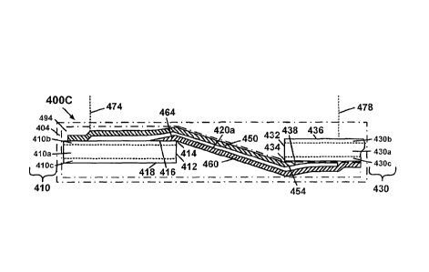
distal end 420s is
electrically connected to the fourth distal end 420t, for example, at second
junction 420u, or by a
linking portion, such that the third portion 420c is configured electrically
in parallel to the second
portion 420b when configured to interconnect with the first solar cell 430.
[0056] With
further reference to FIG. 4B and 4C, in accordance with embodiments of the
present invention, it should be noted that the nature of the parallel
connection between electrically
conductive portions interconnecting a first solar cell and a second solar cell
is such that, for distal
ends of electrically conductive portions not directly joined together, without
limitation thereto, the
metallic substrate of a second solar cell and a TCO layer of the first solar
cell may provide the
necessary electrical coupling. For example, distal ends 420v and 420s are
electrically coupled
23
CA 02718518 2010-09-15
WO 2009/117233 PCT/US2009/035486
through a low resistance connection through a metallic substrate 430c of
second solar cell 430.
Similarly, for example, distal ends 420w and 420q are electrically coupled
through the low
resistance connection through the TCO layer 410b of first solar cell 410.
[0057] With further reference to FIG. 4B, in accordance with embodiments of
the present
invention, an open-circuit defect 440 is shown such that second portion 420b
is conductively
impaired. FIG. 4B illustrates the manner in which the plurality of
electrically conductive portions
420a, 420b, 420c, 420i and 420m is configured such that solar-cell efficiency
is substantially
undiminished in an event that any one of the plurality of electrically
conductive portions 420a,
420b, 420c, 420i and 420m is conductively impaired, for example, second
portion 420b. An arrow
448 indicates the nominal electron-flow through a third portion 420c of the
plurality of electrically
conductive portions 420a, 420b, 420c, 420i and 420m essentially unaffected by
open-circuit defect
440. In the absence of open-circuit defect 440, an electron-flow indicated by
arrow 448 would
normally flow through any one electrically conductive portion of the plurality
of electrically
conductive portions 420a, 420b, 420c, 420i and 420m, in particular, second
portion 420b. However,
when the open-circuit defect 440 is present, this electron-flow divides into
two portions shown by
arrows 442 and 444: arrow 442 corresponding to that portion of the normal
electron-flow flowing to
the right along the second portion 420b to the second solar cell 430, and
arrow 444 corresponding to
that portion of the normal electron-flow flowing to the left along the second
portion 420b to the first
portion 420a and then to the right along the first portion 420a to the second
solar cell 430. Thus, the
net electron-flow represented by arrow 446 flowing to the right along the
first portion 420a is
consequently larger than what would normally flow to the right along the first
portion 420a to the
second solar cell 430 in the absence of the open-circuit defect 440.
[0058] It should be noted that open-circuit defect 440 is for illustration
purposes only and that
embodiments of the present invention compensate for other types of defects in
an electrically
conductive portion, in general, such as, without limitation to: a delamination
of an electrically
24
CA 02718518 2010-09-15
WO 2009/117233
PCT/US2009/035486
conductive portion from the first solar cell 410, corrosion of an electrically
conductive portion, and
even complete loss of an electrically conductive portion. In accordance with
embodiments of the
present invention, in the event a defect completely conductively impairs an
electrically conductive
portion, the physical spacing between adjacent electrically conductive
portions, identified with
double-headed arrow 449, may be chosen such that solar-cell efficiency is
substantially
undiminished. Nevertheless, embodiments of the present invention embrace,
without limitation
thereto, other physical spacings between adjacent electrically conductive
portions in the event
defects are less severe than those causing a complete loss of one of the
electrically conductive
portions.
[0059] With
further reference to FIG. 4B, in accordance with embodiments of the present
invention, the plurality of electrically conductive portions 420a, 420b, 420c,
4201 and 420m may be
connected electrically in series to form a single continuous electrically
conductive line. Moreover,
the trace that includes the plurality of electrically conductive portions
420a, 420b, 420c, 420i and
420m may be disposed in a serpentine pattern such that the interconnect
assembly 420 is configured
to collect current from the first solar cell 410 and to interconnect
electrically to the second solar cell
430, as shown.
[0060] With
further reference to FIG. 4C, in accordance with embodiments of the present
invention, a cross-sectional, elevation view 400C of the interconnect assembly
420 is shown that
further details the physical interconnection of two solar cells 410 and 430 in
the solar-cell module
404. Projections 474 and 478 of planes orthogonal to both of the views in
FIGS. 4B and 4C, and
coincident with the ends of the plurality of electrically conductive portions
420a, 420b, 420c, 4201
and 420m show the correspondence between features of the plan view 400B of
FIG. 4B and features
in the cross-sectional, elevation view 400C of FIG. 4C. Also, it should be
noted that although the
solar-cell module 404 is shown with separation 472 between the first solar
cell 410 and the second
solar cell 430, there need not be such separation 472 between the first solar
cell 410 and the second
CA 02718518 2010-09-15
WO 2009/117233
PCT/US2009/035486
solar cell 430. As shown in FIG. 4B and 4C, a combined solar-cell,
interconnect assembly 494
includes the first solar cell 410 and the interconnect assembly 420. The
interconnect assembly 420
includes the trace disposed above the light-facing side 416 of the first solar
cell 410, the trace
further including the plurality of electrically conductive portions 420a,
420b, 420c, 420i and 420m.
All electrically conductive portions of the plurality of electrically
conductive portions 420a, 420b,
420c, 420i and 420m are configured to collect current from the first solar
cell 410 and to
interconnect electrically to the second solar cell 430. In addition, the
plurality of electrically
conductive portions 420a, 420b, 420c, 420i and 420m may be configured such
that solar-cell
efficiency is substantially undiminished in an event that any one of the
plurality of electrically
conductive portions 420a, 420b, 420c, 420i and 420m is conductively impaired.
Also, any of the
plurality of electrically conductive portions 420a, 420b, 420c, 420i and 420m
may be configured to
interconnect electrically to the second solar cell 430. The first solar cell
410 of the combined solar-
cell, interconnect assembly 494 may include a metallic substrate 410c and an
absorber layer 410a.
The absorber layer 410a of the first solar cell 410 may include copper indium
gallium diselenide
(CIGS). Alternatively, other semiconductors having the chalcopyrite crystal
structure, for example,
chemically homologous compounds with the compound CIGS having the chalcopyrite
crystal
structure, in which alternative elemental constituents are substituted for Cu,
In, Ga, and/or Se, may
be used as the absorber layer 410a. Moreover, in embodiments of the present
invention, it should be
noted that semiconductors, such as silicon and cadmium telluride, as well as
other semiconductors,
may be used as the absorber layer 410a.
[0061] With
further reference to FIG. 4C, in accordance with embodiments of the present
invention, the plurality of electrically conductive portions 420a, 420b, 420c,
420i and 420m of the
combined solar-cell, interconnect assembly 494 further includes the first
portion 420a of the
plurality of electrically conductive portions 420a, 420b, 420c, 420i and 420m
configured to collect
current from the first solar cell 410 and the second portion 420b of the
plurality of electrically
26
CA 02718518 2010-09-15
WO 2009/117233 PCT/US2009/035486
conductive portions 420a, 420b, 420c, 420i and 420m configured to collect
current from the first
solar cell 410. The first portion 420a includes the first end 420p distal from
an edge 414 of the first
solar cell 410. The second portion 420b includes the second end 420q distal
from the edge 414 of
the first solar cell 410. The second portion 420b is disposed proximately to
the first portion 420a
and electrically connected to the first portion 420a such that the first
distal end 420p is electrically
connected to the second distal end 420q such that the second portion 420b is
configured electrically
in parallel to the first portion 420a when configured to interconnect to the
second solar cell 430.
[0062] With further reference to FIG. 4C, in accordance with embodiments of
the present
invention, the interconnect assembly 420 further includes a top carrier film
450. The top carrier film
450 includes a first substantially transparent, electrically insulating layer
coupled to the trace and
disposed above a top portion of the trace. The first substantially
transparent, electrically insulating
layer allows for forming a short-circuit-preventing portion 454 at an edge 434
of the second solar
cell 430. The first substantially transparent, electrically insulating layer
allows for forming the
short-circuit-preventing portion 454 at the edge 434 of the second solar cell
430 to prevent the first
portion 420a from short circuiting an absorber layer 430a of the second solar
cell 430 in the event
that the first portion 420a buckles and rides up a side 432 of second solar
cell 430. The edge 434 is
located at the intersection of the side 432 of the second solar cell 430 and a
back side 438 of the
second solar cell 430 that couples with the plurality of electrically
conductive portions 420a, 420b,
420c, 420i and 420m, for example, first portion 420a as shown. The second
solar cell 430 may
include the absorber layer 430a, a TCO layer 430b, and the metallic substrate
430c; a backing layer
(not shown) may also be disposed between the absorber layer430a and the
metallic substrate 430c.
Above a light-facing side 436 of the second solar cell 430, an integrated
busbar-solar-cell-current
collector (not shown in FIG. 4C, but which is shown in FIGS. 6A and 6B) may be
disposed and
coupled to the second solar cell 430 to provide interconnection with a load
(not shown).
Alternatively, above the light-facing side 436 of the second solar cell 430,
another interconnect
27
CA 02718518 2010-09-15
WO 2009/117233
PCT/US2009/035486
assembly (not shown) may be disposed and coupled to the second solar cell 430
to provide
interconnection with additional solar-cells (not shown) in the solar-cell
module 404.
[0063] With
further reference to FIG. 4C, in accordance with embodiments of the present
invention, the interconnect assembly 420 further includes a bottom carrier
film 460. The bottom
carrier film 460 may include a second electrically insulating layer coupled to
the trace and disposed
below a bottom portion of the trace. Alternatively, The bottom carrier film
460 may include a
carrier film selected from a group consisting of a second electrically
insulating layer, a structural
plastic layer, and a metallic layer, and is coupled to the trace and is
disposed below a bottom portion
of the trace. The second electrically insulating layer allows for forming an
edge-protecting portion
464 at the edge 414 of the first solar cell 410. Alternatively, a
supplementary isolation strip (not
shown) of a third electrically insulating layer may be disposed between the
bottom carrier film 460
and the first portion 420a of the plurality of electrically conductive
portions 420a, 420b, 420c, 420i
and 420m, or alternatively between the bottom carrier film 460 and the edge
414, to provide
additional protection at the edge 414. The supplementary isolation strip may
be as wide as 5
millimeters (mm) in the direction of the double-headed arrow showing the
separation 472, and may
extend along the full length of a side 412 of the first solar cell 410. The
edge 414 is located at the
intersection of the side 412 of the first solar cell 410 and a light-facing
side 416 of the first solar cell
410 that couples with the plurality of electrically conductive portions 420a,
420b, 420c, 420i and
420m, for example, first portion 420a as shown. The first solar cell 410 may
include the absorber
layer 410a, the TCO layer 410b, and the metallic substrate 410c; a backing
layer (not shown) may
also be disposed between the absorber layer410a and the metallic substrate
410c. Below a back side
418 of the first solar cell 410, a first busbar (not shown) may be disposed
and coupled to the first
solar cell 410 to provide interconnection with a load (not shown).
Alternatively, below the back side
418 of the first solar cell 410, another interconnect assembly (not shown) may
be disposed and
28
CA 02718518 2010-09-15
WO 2009/117233 PCT/US2009/035486
coupled to the first solar cell 410 to provide interconnection with additional
solar-cells (not shown)
in the solar-cell module 404.
[0064] With reference now to FIGS. 4D and 4E, in accordance with
embodiments of the
present invention, cross-sectional, elevation views 400D and 400E,
respectively, of two alternative
interconnect assemblies that minimize the separation 472 (see FIG. 4B) between
the first solar cell
410 and the second solar cell 430 to improve the solar-cell-module efficiency
of the solar-cell
module 404 are shown. In both examples shown in FIGS. 4D and 4E, the side 412
of the first solar
cell 410 essentially coincides with the side 432 of the second solar cell 430.
It should be noted that
as used herein the phrase, "essentially coincides," with respect to the side
412 of the first solar cell
410 and the side 432 of the second solar cell 430 means that there is little
or no separation 472
between the first solar cell 410 and the second solar cell 430, and little or
no overlap of the first
solar cell 410 with the second solar cell 430 so that there is less wasted
space and open area between
the solar cells 410 and 430, which improves the solar-collection efficiency of
the solar-cell module
404 resulting in improved solar-cell-module efficiency. FIG. 4D shows an edge-
conforming
interconnect assembly for the physical interconnection of the two solar cells
410 and 430 in the
solar-cell module 404. FIG. 4E shows a shingled-solar-cell arrangement for the
physical
interconnection of the two solar cells 410 and 430 in the solar-cell module
404. For both the edge-
conforming interconnect assembly of FIG. 4D and the shingled-solar-cell
arrangement of FIG. 4E,
the interconnect assembly 420 further includes the bottom carrier film 460.
The bottom carrier film
460 includes a second electrically insulating layer coupled to the trace and
disposed below a bottom
portion of the trace. Alternatively, The bottom carrier film 460 may include a
carrier film selected
from a group consisting of a second electrically insulating layer, a
structural plastic layer, and a
metallic layer, and is coupled to the trace and is disposed below a bottom
portion of the trace. The
second electrically insulating layer allows for forming the edge-protecting
portion 464 at the edge
414 of the first solar cell 410. In the case of the edge-conforming
interconnect assembly shown in
29
CA 02718518 2010-09-15
WO 2009/117233 PCT/US2009/035486
FIG. 4D, the bottom carrier film 460 and the first portion 420a of the
interconnect assembly 420
may be relatively flexible and compliant allowing them to wrap around the edge
414 and down the
side 412 of the first solar cell 410, as shown. The edge 414 is located at the
intersection of the side
412 of the first solar cell 410 and the light-facing side 416 of the first
solar cell 410 that couples
with the plurality of electrically conductive portions 420a, 420b, 420c, 420i
and 420m, for example,
first portion 420a as shown. The first solar cell 410 may include the absorber
layer 410a, a TCO
layer 410b, and the metallic substrate 410c; a backing layer (not shown) may
also be disposed
between the absorber layer 410a and the metallic substrate 410c. Below the
back side 418 of the
first solar cell 410, another interconnect assembly (not shown) or first
busbar (not shown) may be
disposed and coupled to the first solar cell 410 as described above for FIG.
4C. If an additional solar
cell (not shown) is interconnected to the back side 418 of the first solar
cell 410 as in the shingled-
solar-cell arrangement of FIG. 4E, the first solar cell 410 would be pitched
upward at its left-hand
side and interconnected to another interconnect assembly similar to the manner
in which the second
solar cell 430 is shown interconnected with solar cell 410 at side 412 in FIG.
4E.
[0065] With further reference to FIGS. 4D and 4E, in accordance with
embodiments of the
present invention, the interconnect assembly 420 further includes the top
carrier film 450. The top
carrier film 450 includes a first substantially transparent, electrically
insulating layer coupled to the
trace and disposed above a top portion of the trace. The first substantially
transparent, electrically
insulating layer allows for forming the short-circuit-preventing portion 454
at the edge 434 of the
second solar cell 430 to prevent the first portion 420a from short circuiting
the absorber layer 430a
of the second solar cell 430 in the event that the first portion 420a rides up
the side 432 of second
solar cell 430. The edge 434 is located at the intersection of the side 432 of
the second solar cell 430
and the back side 438 of the second solar cell 430 that couples with the
plurality of electrically
conductive portions 420a, 420b, 420c, 420i and 420m, for example, first
portion 420a as shown. In
the case of the edge-conforming interconnect assembly shown in FIG. 4D, the
top carrier film 450
CA 02718518 2010-09-15
WO 2009/117233 PCT/US2009/035486
may be relatively flexible and compliant allowing it to follow the
conformation of the bottom carrier
film 460 and the first portion 420a of the interconnect assembly 420
underlying it that wrap around
the edge 414 and down the side 412 of the first solar cell 410, as shown. The
second solar cell 430
may include the absorber layer 430a, the TCO layer 430b, and the metallic
substrate 430c; a
backing layer (not shown) may also be disposed between the absorber layer430a
and the metallic
substrate 430c. Also, in the case of the edge-conforming interconnect
assembly, the absorber layer
430a, TCO layer 430b, and metallic substrate 430c of the second solar cell 430
may be relatively
flexible and compliant allowing them to follow the conformation of the
underlying interconnect
assembly 420 that wraps around the edge 414 and down the side 412 of the first
solar cell 410.
Above the light-facing side 436 of the second solar cell 430, an integrated
busbar-solar-cell-current
collector (not shown in FIG. 4C, but which is shown in FIGS. 6A and 6B), or
alternatively another
interconnect assembly (not shown), may be disposed on and coupled to the
second solar cell 430, as
described above for FIG. 4C.
[0066] With reference now to FIG. 4F, in accordance with embodiments of the
present
invention, a plan view 400F of an alternative interconnect assembly for the
interconnect assembly
420 of FIG. 4A is shown that details the physical interconnection of two solar
cells 410 and 430 in
the solar-cell module 404. The solar-cell module 404 includes the first solar
cell 410, at least the
second solar cell 430 and the interconnect assembly 420 disposed above the
light-facing side 416 of
the absorber layer of the first solar cell 410. The edges 414 and 434 of the
solar cells 410 and 430
may be separated by the separation 472 as shown in FIG. 4F; or alternatively,
the edges 414 and 434
of the solar cells 410 and 430 may essentially coincide as discussed above for
FIGS. 4D and 4E.
The interconnect assembly 420 includes a trace comprising a plurality of
electrically conductive
portions 420a, 420b, 420c, 420i and 420m, previously identified herein with
the resistors 420a,
420b, 420c, 420i and 420m described in FIG. 400A, where the ellipsis of 420i
indicates additional
electrically conductive portions (not shown). The plurality of electrically
conductive portions 420a,
31
CA 02718518 2010-09-15
WO 2009/117233
PCT/US2009/035486
420b, 420c, 420i and 420m is configured both to collect current from the first
solar cell 410 and to
interconnect electrically to the second solar cell 430. The plurality of
electrically conductive
portions 420a, 420b, 420c, 420i and 420m is configured such that solar-cell
efficiency is
substantially undiminished in an event that any one of the plurality of
electrically conductive
portions 420a, 420b, 420c, 420i and 420m is conductively impaired.
[0067] With
further reference to FIG. 4F, in accordance with embodiments of the present
invention, the detailed configuration of the plurality of electrically
conductive portions 420a, 420b,
420c, 420i and 420m is shown without electrically connecting trace portions,
for example, junctions
formed in the trace or linking portions of the trace. For example, in the case
where electrically
connecting trace portions of the trace have been cut away, removed, or are
otherwise absent, from
the distal ends of the plurality of electrically conductive portions 420a,
420b, 420c, 420i and 420m,
as shown in FIG. 4F. The plurality of electrically conductive portions 420a,
420b, 420c, 420i and
420m may be linked together instead indirectly by the TCO layer 410b of the
first solar cell 410 at
distal ends of the trace disposed over the first solar cell 410, for example,
first distal end 420p of
first portion 420a and second distal end 420q of second portion 420b by
portions of the TCO layer
410b of the first solar cell 410 that lie in between the distal ends 420p and
420q. In like fashion, the
distal ends 420w and 420q are electrically coupled through the low resistance
connection through
the TCO layer 410b of first solar cell 410. Similarly, the plurality of
electrically conductive portions
420a, 420b, 420c, 420i and 420m may be linked together instead indirectly by
the metallic substrate
430c, or intervening backing layer (not shown), of the first solar cell 430 at
distal ends of the trace
disposed under the second solar cell 430, for example, third distal end 420s
of second portion 420b
and fourth distal end 420t of third portion 420c by portions of the metallic
substrate 430c of the
second solar cell 430 that lie in between the distal ends 420s and 420t. In
like fashion, the distal
ends 420v and 420s are electrically coupled through a low resistance
connection through the
metallic substrate 430c of second solar cell 430.
32
CA 02718518 2010-09-15
WO 2009/117233 PCT/US2009/035486
[0068] With further reference to FIG. 4F, in accordance with embodiments of
the present
invention, the open-circuit defect 440 is shown such that second portion 420b
is conductively
impaired. FIG. 4F illustrates the manner in which the plurality of
electrically conductive portions
420a, 420b, 420c, 420i and 420m is configured such that solar-cell efficiency
is substantially
undiminished in an event that any one of the plurality of electrically
conductive portions 420a,
420b, 420c, 420i and 420m is conductively impaired, for example, second
portion 420b. An arrow
480 indicates the nominal electron-flow through an m-th portion 420m of the
plurality of
electrically conductive portions 420a, 420b, 420c, 420i and 420m essentially
unaffected by open-
circuit defect 440. In the absence of open-circuit defect 440, an electron-
flow indicated by arrow
480 would normally flow through any one electrically conductive portion of the
plurality of
electrically conductive portions 420a, 420b, 420c, 420i and 420m, in
particular, second portion
420b. However, when the open-circuit defect 440 is present, portions of this
electron-flow are lost
to adjacent electrically conductive portions 420a and 420c shown by arrows
484a and 484c; arrow
482 corresponds to that portion of the normal electron-flow flowing to the
right along the second
portion 420b to the second solar cell 430, and arrow 484b corresponds to that
portion of the normal
electron-flow that would bridge the open-circuit defect 440 by flowing through
the higher resistance
path of the TCO layer 410b bridging across the two portions of second portion
420b on either side
of the open-circuit defect 440. Thus, the net electron-flow represented by
arrow 486 flowing to the
right along the first portion 420a is consequently larger than what would
normally flow to the right
along the first portion 420a to the second solar cell 430 in the absence of
the open-circuit defect
440; and, the net electron-flow represented by arrow 488 flowing to the right
along the third portion
420c is consequently larger than what would normally flow to the right along
the third portion 420c
to the second solar cell 430 in the absence of the open-circuit defect 440.
[0069] Moreover, in the case of the alternative interconnect assembly
depicted in FIG. 4F, as
stated before for the interconnect assembly depicted in FIG. 4B, it should
again be noted that open-
33
CA 02718518 2010-09-15
WO 2009/117233 PCT/US2009/035486
circuit defect 440 is for illustration purposes only and that embodiments of
the present invention
compensate for other types of defects in an electrically conductive portion,
in general, such as,
without limitation to: a delamination of an electrically conductive portion
from the first solar cell
410, corrosion of an electrically conductive portion, and even complete loss
of an electrically
conductive portion. In accordance with embodiments of the present invention,
in the event a defect
completely conductively impairs an electrically conductive portion, the
physical spacing between
adjacent electrically conductive portions, identified with double-headed arrow
449, may be chosen
such that solar-cell efficiency is substantially undiminished. Nevertheless,
embodiments of the
present invention embrace, without limitation thereto, other physical spacings
between adjacent
electrically conductive portions in the event defects are less severe than
those causing a complete
loss of one of the electrically conductive portions.
[0070] With reference now to FIG. 5A, in accordance with embodiments of the
present
invention, a plan view 500A of the combined applicable carrier film,
interconnect assembly 504 is
shown. FIG. 5A shows the physical arrangement of a trace 520 with respect to a
top carrier film 550
and a bottom carrier film 560 in the combined applicable carrier film,
interconnect assembly 504.
The combined applicable carrier film, interconnect assembly 504 includes the
top carrier film 550
and the trace 520 including a plurality of electrically conductive portions
520a, 520b, 520c, 520d,
520e, 520f, 520g, 520m and 520i, the latter corresponding to the ellipsis
indicating additional
electrically conductive portions (not shown). The plurality of electrically
conductive portions 520a
through 520m is configured both to collect current from a first solar cell 510
(shown in FIG. 5C)
and to interconnect electrically to a second solar cell (not shown). As shown
in FIG. 5A, the
plurality of electrically conductive portions 520a through 520m run over the
top of the first solar
cell 510 on the left and over an edge 514 of the first solar cell 510 to the
right under an edge 534 of,
and underneath, the second solar cell (not shown). The top carrier film 550
includes a first
substantially transparent, electrically insulating layer 550A (shown in FIG.
5B). The plurality of
34
CA 02718518 2010-09-15
WO 2009/117233 PCT/US2009/035486
electrically conductive portions 520a through 520m is configured such that
solar-cell efficiency is
substantially undiminished in an event that any one of the plurality of
electrically conductive
portions 520a through 520m is conductively impaired. It should be noted that
as used herein the
phrase, "substantially transparent," with respect to a substantially
transparent, electrically insulating
layer means that light passes through the substantially transparent,
electrically insulating layer with
negligible absorption. The first substantially transparent, electrically
insulating layer 550a is
coupled to the trace 520 and disposed above a top portion of the trace 520
(shown in FIG. 5B) as
indicated by the dashed portions of the trace 520 on the left of FIG. 5A.
[00711 With reference now to FIGS.5B and 5C, in accordance with embodiments
of the
present invention, a cross-sectional, elevation view of the combined
applicable carrier film,
interconnect assembly 504 of FIG. 5A is shown. As shown in FIGS. 5B and 5C,
the cross-section of
the view is taken along a cut parallel to the edge 514 of the first solar cell
510. The cross-sectional,
elevation view of FIG. 5B shows the physical arrangement of the trace 520 with
respect to the top
carrier film 550 in the combined applicable carrier film, interconnect
assembly 504 prior to
disposition on the first solar cell 510. On the other hand, the cross-
sectional, elevation view of FIG.
5C shows the physical arrangement of the trace 520 with respect to the top
carrier film 550 and the
first solar cell 510 of the combined applicable carrier film, interconnect
assembly 504 after it
couples with the first solar cell 510. The top carrier film 550 and the trace
520 are configured for
applying to a light-facing side of the first solar cell 510 both to collect
current from the first solar
cell 510 and to interconnect electrically to the second solar cell (not
shown). The first solar cell 510
may include an absorber layer 510a, a TCO layer 510b, and a metallic substrate
510c; the backing
layer (not shown) may also be disposed between the absorber layer 510a and the
metallic substrate
510c. The first substantially transparent, electrically insulating layer 550a
holds the trace 520 down
in contact with the first solar cell 510 and allows for forming a short-
circuit-preventing portion at an
edge of the second solar cell (not shown). The top carrier film 550 further
includes a first
CA 02718518 2010-09-15
WO 2009/117233 PCT/US2009/035486
substantially transparent, adhesive medium 550b coupling the trace 520 to the
substantially
transparent, electrically insulating layer 550a. As shown in FIG. 5B, prior to
disposition on the first
solar cell 510, the top carrier film 550 lies relatively flat across the top
portion of the trace 520, for
example, as for the conformational state of the top carrier film 550
immediately after roll-to-roll
fabrication of the combined applicable carrier film, interconnect assembly
504. In contrast, after
disposition on the first solar cell 510, the top carrier film 550 conforms to
the top portion of the
trace 520, as shown in FIG. 5B. The first substantially transparent, adhesive
medium 550b allows
for coupling the trace 520 to the first solar cell 510 without requiring
solder. The first substantially
transparent, electrically insulating layer 550a may include a structural
plastic material, such as
polyethylene terephthalate (PET). In accordance with embodiments of the
present invention, a first
substantially transparent, adhesive medium such as first substantially
transparent, adhesive medium
550b may be included, without limitation thereto, in a top carrier film of:
the combined applicable
carrier film, interconnect assembly 504, the interconnect assembly 320, the
integrated busbar-solar-
cell-current collector 690 (see FIG. 6B), the combined solar-cell,
interconnect assembly 494, or the
interconnect assembly 420 of the solar-cell module 404.
[0072] With further reference to FIGS. 5A, 5B and 5C, in accordance with
embodiments of
the present invention, the combined applicable carrier film, interconnect
assembly 504 further
includes the bottom carrier film 560. The bottom carrier film 560 includes a
second electrically
insulating layer, like 550a, coupled to the trace 520 and disposed below a
bottom portion of the
trace 520, as indicated by the solid-line portions of the trace 520 on the
right of FIG. 5A.
Alternatively, the bottom carrier film 560 may include a carrier film selected
from a group
consisting of a second electrically insulating layer, a structural plastic
layer, and a metallic layer,
and is coupled to the trace 520 and is disposed below a bottom portion of the
trace 520. The second
electrically insulating layer, like 550a, holds the trace 520 down in contact
with a back side of the
second solar cell (not shown) and allows for forming an edge-protecting
portion at the edge 514 of
36
CA 02718518 2010-09-15
WO 2009/117233 PCT/US2009/035486
the first solar cell 510. The bottom carrier film 560 further includes a
second adhesive medium, like
550b, coupling the trace to the second electrically insulating layer, like
550a. The second adhesive
medium, like 550b, allows for coupling the trace 520 to the back side of the
second solar cell (not
shown) without requiring solder. The second electrically insulating layer,
like 550a, includes a
structural plastic material, such as PET. In accordance with embodiments of
the present invention, a
second adhesive medium, like 550b, may be included, without limitation
thereto, in a bottom carrier
film of: the combined applicable carrier film, interconnect assembly 504, the
interconnect assembly
320, the combined solar-cell, interconnect assembly 494, or the interconnect
assembly 420 of the
solar-cell module 404.
[0073] With further reference to FIGS. 5A, in accordance with embodiments
of the present
invention, the trace 520 may be disposed in a serpentine pattern that allows
for collecting current
from the first solar cell 510 (shown in FIG. 5C) and electrically
interconnecting to the second solar
cell (not shown). It should be noted that neither the first solar cell 510 nor
the second solar cell (not
shown) are shown in FIG. 5A so as not to obscure the structure of the combined
applicable carrier
film, interconnect assembly 504. As shown in FIG. 5A, the combined applicable
carrier film,
interconnect assembly 504 includes the trace 520 including the plurality of
electrically conductive
portions 520a through 520m that may run in a serpentine pattern back and forth
between the first
solar cell 510 and the second solar cell (not shown). The serpentine pattern
is such that adjacent
electrically conductive portions of the plurality of electrically conductive
portions 520a through
520m are configured in pairs of adjacent electrically conductive portions:
520a and 520b, 520c and
520d, 520e and 520f, etc. The pairs of adjacent electrically conductive
portions may be configured
in a regular repeating pattern of equally spaced adjacent electrically
conductive portions. The trace
520 including the plurality of electrically conductive portions 520a through
520m is disposed
between the top carrier film 550 disposed above a top portion of the trace 520
and the bottom carrier
film 560 disposed below a bottom portion of the trace 520. The first
substantially transparent,
37
CA 02718518 2010-09-15
WO 2009/117233 PCT/US2009/035486
electrically insulating layer 550a of top carrier film 550 and the second
electrically insulating layer,
or alternatively, structural plastic layer or metallic layer, of bottom
carrier film 560 are coupled to
the trace 520 with a first substantially transparent, adhesive medium 550b and
second adhesive
medium which also serve to couple the trace 520 to the first solar cell 510,
which may be located on
the left, and the second solar cell, which may be located on the right. In the
space between the two
solar cells, between the edge 514 of the first solar cell and the edge 534 of
the second solar cell, the
trace is sandwiched between the two carrier films 550 and 560; the overlapping
region of the two
carrier films 550 and 560 extends somewhat beyond the respective edges 514 and
534 of the first
and second solar cells so as to form, respectively, an edge-protecting portion
at the edge 514 of the
first solar cell, and a short-circuit-preventing portion at the edge 534 of
the second solar cell, from
the trace 520 that crosses the edges 514 and 534.
[0074] With further reference to FIGS. 5B and 5C, in accordance with
embodiments of the
present invention, the trace 520 may further include an electrically
conductive line including a
conductive core 520A with at least one overlying layer 520B. In one embodiment
of the present
invention, the electrically conductive line may include the conductive core
520A including a
material having greater conductivity than nickel, for example, copper, with an
overlying nickel layer
520B. In another embodiment of the present invention, electrically conductive
line may include the
conductive core 520A including nickel without the overlying layer 520B. The
electrically
conductive line may also be selected from a group consisting of a copper
conductive core clad with
a silver cladding, a copper conductive core clad with a nickel coating further
clad with a silver
cladding and an aluminum conductive core clad with a silver cladding.
[0075] With further reference to FIG. 5B and 5C, in accordance with
embodiments of the
present invention, the trace 520 for collecting current from a solar cell, for
example the first solar
cell 510, may include an electrically conductive line including the conductive
core 520A, and the
overlying layer 520B that limits current flow to a proximate shunt defect (not
shown) in the solar
38
CA 02718518 2010-09-15
WO 2009/117233 PCT/US2009/035486
cell. The proximate shunt defect may be proximately located in the vicinity of
an electrical contact
between the overlying layer 520B of the electrically conductive line and the
TCO layer 510b of the
solar cell, for example, first solar cell 510. The overlying layer 520B of the
electrically conductive
line of the trace 520 may further include an overlying layer 520B composed of
nickel. The
conductive core 520A of the electrically conductive line of the trace 520 may
further include nickel.
The conductive core 520A may also include a material selected from a group
consisting of copper,
silver, aluminum, and elemental constituents and alloys having high electrical
conductivity, which
may be greater than the electrical conductivity of nickel. The TCO layer 510b
of the solar cell, for
example first solar cell 510, may include a conductive oxide selected from a
group consisting of
zinc oxide, aluminum zinc oxide and indium tin oxide. In addition, the
absorber layer 510a, for
example, absorber layer 112 of FIG. 1A, of the solar cell, for example, first
solar cell 510, may
include copper indium gallium diselenide (CIGS). Alternatively, in embodiments
of the present
invention, it should be noted that semiconductors, such as silicon, cadmium
telluride, and
chalcopyrite semiconductors, as well as other semiconductors, may be used as
the absorber layer
510a. Moreover, an n-type layer, for example, n-type portion 112b of absorber
layer 112 of FIG.
1A, of the solar cell, for example, first solar cell 510, may be disposed on
and electrically coupled to
a p-type absorber layer, for example, absorber layer 112 of FIG. 1A, of the
solar cell, for example,
first solar cell 510, and the n-type layer, for example, n-type portion 112b
of absorber layer 112 of
FIG. 1A, may be selected from a group consisting of a metal oxide, a metal
sulfide and a metal
selenide.
100761 Although the trace 520 is shown as having a circular cross-section
having a point-like
contact with a solar cell, for example, with the TCO layer 510b, or, without
limitation thereto, to a
top surface, of the first solar cell 510, embodiments of the present
inventions include, without
limitation thereto, other cross-sectional profiles of the trace 520, such as a
profile including a
flattened top portion and a flattened bottom portion, so as to increase the
contact area between the
39
CA 02718518 2010-09-15
WO 2009/117233 PCT/US2009/035486
trace 520 and a solar cell with which it makes contact. For example, a
flattened bottom portion of
trace 520 increases the contact area with the light-facing side of the first
solar cell 510; on the other
hand, a flattened top portion of trace 520 increases the contact area with a
back side of an adjacent
solar cell to which the plurality of electrically conductive portions 520a
through 520m of the trace
520 interconnects. In accordance with embodiments of the present invention, a
trace, such as trace
520, may be included, without limitation thereto, in: the combined applicable
carrier film,
interconnect assembly 504, the interconnect assembly 320, the integrated
busbar-solar-cell-current
collector 690 (see FIG. 6B), the combined solar-cell, interconnect assembly
494, or the interconnect
assembly 420 of the solar-cell module 404.
[0077] With reference now to FIG. 6A, in accordance with embodiments of the
present
invention, a plan view 600A of an integrated busbar-solar-cell-current
collector 690 is shown. FIG.
6A shows the physical interconnection of a terminating solar cell 660 with a
terminating busbar 680
of the integrated busbar-solar-cell-current collector 690. The integrated
busbar-solar-cell-current
collector 690 includes the terminating busbar 680 and an integrated solar-
cell, current collector 670.
The integrated solar-cell, current collector 670 includes a plurality of
integrated pairs 670a&b,
670c&d, 670e&f, 670g&h, and 6701&m and 670i, the ellipsis indicating
additional integrated pairs
(not shown), of electrically conductive, electrically parallel trace portions
670a-m. Throughout the
following, the respective integrated pairs: 670a and 670b, 670c and 670d, 670e
and 670f, 670g and
670h, and 6701 and 670m, are referred to respectively as: 670a&b, 670c&d,
670e&f, 670g&h, and
6701&m; and the electrically conductive, electrically parallel trace portions:
670a, 670b, 670c, 670d,
670e, 670f, 670g, 670h, 6701 and 670m, are referred to as 670a-m. The
plurality of integrated pairs
670a&b, 670c&c, 670e&f, 670g&h, 670i and 6701&m of electrically conductive,
electrically
parallel trace portions 670a-m is configured both to collect current from the
terminating solar cell
660 and to interconnect electrically to the terminating busbar 680. The
plurality of integrated pairs
670a&b, 670c&c, 670e&f, 670g&h, 670i and 6701&m of electrically conductive,
electrically
CA 02718518 2010-09-15
WO 2009/117233
PCT/US2009/035486
parallel trace portions 670a-m is configured such that solar-cell efficiency
is substantially
undiminished in an event that any one electrically conductive, electrically
parallel trace portion, for
example, 670h, of the plurality of integrated pairs 670a&b, 670c&c, 670e&f,
670g&h, 670i and
6701&m of electrically conductive, electrically parallel trace portions 670a-m
is conductively
impaired.
10078] With
further reference to FIG. 6A and 6B, in accordance with embodiments of the
present invention, the plurality of integrated pairs 670a&b, 670c&c, 670e&f,
670g&h, 670i and
6701&m of electrically conductive, electrically parallel trace portions 670a-m
further includes a first
electrically conductive, electrically parallel trace portion 670a of a first
integrated pair 670a&b of
the electrically conductive, electrically parallel trace portions 670a-m
configured both to collect
current from the terminating solar cell 660 and to interconnect electrically
to the terminating busbar
680, and a second electrically conductive, electrically parallel trace portion
670b of the first
integrated pair 670a&b of the electrically conductive, electrically parallel
trace portions 670a-m
configured both to collect current from the terminating solar cell 660 and to
interconnect electrically
to the terminating busbar 680. The first electrically conductive, electrically
parallel trace portion
670a includes a first end 670p distal from the terminating busbar 680 located
parallel to a side 662
of the terminating solar cell 660. The second electrically conductive,
electrically parallel trace
portion 670b includes a second end 670q distal from the terminating busbar
680. The second
electrically conductive, electrically parallel trace portion 670b is disposed
proximately to the first
electrically conductive, electrically parallel trace portion 670a and
electrically connected to the first
electrically conductive, electrically parallel trace portion 670a such that
the first distal end 670p is
electrically connected to the second distal end 670q, for example, at first
junction 670r, or by a
linking portion, such that the second electrically conductive, electrically
parallel trace portion 670b
is configured electrically in parallel to the first electrically conductive,
electrically parallel trace
portion 670a when configured to interconnect to the terminating busbar 680. In
addition, in
41
CA 02718518 2010-09-15
WO 2009/117233
PCT/US2009/035486
accordance with embodiments of the present invention, the terminating busbar
680 may be disposed
above and connected electrically to extended portions, for example, 670x and
670y, of the plurality
of integrated pairs 670a&b, 670c&c, 670e&f, 670g&h, 670i and 6701&m of
electrically conductive,
electrically parallel trace portions 670a-m configured such that the
terminating busbar 680 is
configured to reduce shadowing of the terminating solar cell 660.
[0079] With
further reference to FIG. 6A, in accordance with embodiments of the present
invention, an open-circuit defect 640 is shown such that eighth electrically
conductive, electrically
parallel trace portion 670h is conductively impaired. FIG. 6A illustrates the
manner in which the
plurality of integrated pairs 670a&b, 670c&c, 670e&f, 670g&h and 6701&m of
electrically
conductive, electrically parallel trace portions 670a-m is configured such
that solar-cell efficiency is
substantially undiminished in an event that any one electrically conductive,
electrically parallel trace
portion, for example, eighth electrically conductive, electrically parallel
trace portion 670h, of the
plurality of integrated pairs 670a&b, 670c&c, 670e&f, 670g&h and 6701&m of
electrically
conductive, electrically parallel trace portions 670a-m is conductively
impaired. The arrow 648
indicates the nominal electron-flow through a sixth electrically conductive,
electrically parallel trace
portion 670f of the plurality of integrated pairs 670a&b, 670c&c, 670e&f,
670g&h and 6701&m of
electrically conductive, electrically parallel trace portions 670a-m
essentially unaffected by open-
circuit defect 640. In the absence of open-circuit defect 640, an electron-
flow indicated by arrow
648 would normally flow through any one electrically conductive, electrically
parallel trace portion
of the plurality of integrated pairs 670a&b, 670c&c, 670e&f, 670g&h and 6701&m
of electrically
conductive, electrically parallel trace portions 670a-m, in particular, eighth
electrically conductive,
electrically parallel trace portion 670h. However, when the open-circuit
defect 640 is present, this
electron-flow divides into two portions shown by arrows 642 and 644: arrow 642
corresponding to
that portion of the normal electron-flow flowing to the right along the eighth
electrically conductive,
electrically parallel trace portion 670h to the terminating busbar 680, and
arrow 644 corresponding
42
CA 02718518 2010-09-15
WO 2009/117233 PCT/US2009/035486
to that portion of the normal electron-flow flowing to the left along the
eighth electrically
conductive, electrically parallel trace portion 670h to the seventh
electrically conductive, electrically
parallel trace portion 670g and then to the right along the seventh
electrically conductive,
electrically parallel trace portion 670g to the terminating busbar 680. Thus,
the net electron-flow
represented by arrow 646 flowing to the right along the seventh electrically
conductive, electrically
parallel trace portion 670g is consequently larger than what would normally
flow to the right along
the seventh electrically conductive, electrically parallel trace portion 670g
to the terminating busbar
680 in the absence of the open-circuit defect 640. It should be noted that
open-circuit defect 640 is
for illustration purposes only and that embodiments of the present invention
compensate for other
types of defects in an electrically conductive, electrically parallel trace
portion, in general, such as,
without limitation to: a delamination of an electrically conductive,
electrically parallel trace portion
from the terminating solar cell 660, corrosion of an electrically conductive,
electrically parallel trace
portion, and even complete loss of an electrically conductive, electrically
parallel trace portion. In
accordance with embodiments of the present invention, in the event a defect
completely
conductively impairs an electrically conductive, electrically parallel trace
portion, the physical
spacing between adjacent electrically conductive, electrically parallel trace
portions, identified with
double-headed arrow 649, may be chosen such that solar-cell efficiency is
substantially
undiminished. Nevertheless, embodiments of the present invention embrace,
without limitation
thereto, other physical spacings between adjacent electrically conductive,
electrically parallel trace
portions in the event defects are less severe than those causing a complete
loss of one of the
electrically conductive, electrically parallel trace portions.
[0080] With reference now to FIG. 6B and further reference to FIG. 6A, in
accordance with
embodiments of the present invention, a cross-sectional, elevation view 600B
of the integrated
busbar-solar-cell-current collector 690 of FIG. 6A is shown. FIG. 6B shows the
physical
interconnection of the terminating solar cell 660 with the terminating busbar
680 in the integrated
43
CA 02718518 2010-09-15
WO 2009/117233
PCT/US2009/035486
busbar-solar-cell-current collector 690. In accordance with embodiments of the
present invention,
the interconnection approach employing a carrier film is also conducive to
coupling the integrated
busbar-solar-cell-current collector 690 directly to the terminating busbar 680
without requiring
solder. Thus, the integrated busbar-solar-cell-current collector 690 further
includes a top carrier film
650. The top carrier film 650 includes a first substantially transparent,
electrically insulating layer
(not shown, but like 550a of FIG. 5B) coupled to the plurality of integrated
pairs 670a&b, 670c&c,
670e&f, 670g&h, 670i and 6701&m of electrically conductive, electrically
parallel trace portions
670a-m, for example, electrically conductive, electrically parallel trace
portion 670a, and disposed
above a top portion of the plurality of integrated pairs 670a&b, 670c&c,
670e&f, 670g&h, 670i and
6701&m of electrically conductive, electrically parallel trace portions 670a-
m.
[0081] With
further reference to FIG. 6A and 6B, in accordance with embodiments of the
present invention, the top carrier film 650 further includes a first adhesive
medium (not shown, but
like 550b of FIGS. 5B and 5C) coupling the plurality of integrated pairs
670a&b, 670c&c, 670e&f,
670g&h, 670i and 6701&m of electrically conductive, electrically parallel
trace portions 670a-m to
the electrically insulating layer (like 550a of FIG. 5B). The first adhesive
medium (like 550b of
FIGS. 5B and 5C) allows for coupling the plurality of integrated pairs 670a&b,
670c&c, 670e&f,
670g&h, 670i and 6701&m of electrically conductive, electrically parallel
trace portions 670a-m to
the terminating solar cell 660 without requiring solder. The terminating solar
cell 660 may include
an absorber layer 660a, a TCO layer 660b, and a metallic substrate 660c; a
backing layer (not
shown) may also be disposed between the absorber layer 660a and the metallic
substrate 660c. The
plurality of integrated pairs of electrically conductive, electrically
parallel trace portions 670a-m
may be connected electrically in series to form a single continuous
electrically conductive line (not
shown). The single continuous electrically conductive line may be disposed in
a serpentine pattern
(not shown, but like the pattern of trace 520 in FIG. 5A) such that the
integrated busbar-solar-cell-
current collector 690 is configured to collect current from the terminating
solar cell 660 and to
44
CA 02718518 2010-09-15
WO 2009/117233
PCT/US2009/035486
interconnect electrically to the terminating busbar 680. The plurality of
integrated pairs 670a&b,
670c&c, 670e&f, 670g&h, 670i and 6701&m of electrically conductive,
electrically parallel trace
portions 670a-m may further include a plurality of electrically conductive
lines (not shown, but like
trace 520 of FIG. 5B and 5C), any electrically conductive line of the
plurality of electrically
conductive lines selected from a group consisting of a copper conductive core
clad with a silver
cladding, a copper conductive core clad with a nickel coating further clad
with a silver cladding and
an aluminum conductive core clad with a silver cladding.
[0082] With
further reference to FIG. 6A and 6B, in accordance with embodiments of the
present invention, integrated busbar-solar-cell-current collector 690 may
include a supplementary
isolation strip (not shown) at an edge 664 of the terminating solar cell 660
and running along the
length of the side 662 to provide additional protection at the edge 664 and
side 662 of the
terminating solar cell 660 from the extended portions, for example, 670x and
670y, of the plurality
of integrated pairs 670a&b, 670c&c, 670e&f, 670g&h, 670i and 6701&m of
electrically conductive,
electrically parallel trace portions 670a-m. In another embodiment of the
present invention, the
extended portions, for example, 670x and 670y, may be configured (not shown)
to provide stress
relief and to allow folding the terminating busbar 680 along edge 664 under a
back side 668 and at
the side 662 of terminating solar cell 660, so that there is less wasted space
and open area between
the terminating solar cell 660 of one module and the initial solar cell (not
shown) of an adjacent
module. Moreover, integrated busbar-solar-cell-current collector 690 may
include a supplementary
carrier-film strip (not shown) at the edge 664 of the terminating solar cell
660 and running along the
length of the side 662 disposed above and coupled to top carrier film 650 and
the terminating busbar
680 to affix the terminating busbar 680 to the extended portions, for example,
670x and 670y.
Alternatively, the integrated busbar-solar-cell-current collector 690 may
include the top carrier film
650 extending over the top of the terminating busbar 680 and extended
portions, for example, 670x
and 670y, to affix the terminating busbar 680 to these extended portions.
Thus, these latter two
CA 02718518 2010-09-15
WO 2009/117233 PCT/US2009/035486
embodiments of the present invention provide a laminate including the
terminating busbar 680
disposed between top carrier film 650, or alternatively the supplementary
carrier-film strip, and the
supplementary isolation strip (not shown) along the edge 664 and side 662 of
the terminating solar
cell 660. Moreover, the top carrier film 650, or the supplementary carrier-
film strip, is conducive to
connecting the terminating busbar 680 without requiring solder to the
plurality, itself, or to the
extended portions, for example, 670x and 670y, of the plurality of integrated
pairs 670a&b, 670c&c,
670e&f, 670g&h, 670i and 6701&m of electrically conductive, electrically
parallel trace portions
670a-m
[0083] With reference now to FIG. 7A, in accordance with embodiments of the
present
invention, a combined cross-sectional elevation and perspective view of a roll-
to-roll, interconnect-
assembly fabricator 700A is shown. FIG. 7A shows the roll-to-roll,
interconnect-assembly
fabricator 700A operationally configured to fabricate an interconnect assembly
720. A top carrier
film 716 including an electrically insulating layer, for example a first
substantially transparent,
electrically insulating layer, is provided to roll-to-roll, interconnect-
assembly fabricator 700A in roll
form from a first roll of material 714. The roll-to-roll, interconnect-
assembly fabricator 700A
includes an first unwinding spool 710 upon which the first roll of material
714 of the top carrier film
716 including the electrically insulating layer is mounted. As shown, a
portion of the first roll of
material 714 is unrolled. The unrolled portion of the top carrier film 716
including the electrically
insulating layer passes to the right and is taken up on a take-up spool 718
upon which it is rewound
as a third roll 722 of interconnect assembly 720, after conductive-trace
material 750 is provided
from a dispenser 754 and is laid down onto the unrolled portion of the top
carrier film 716 including
the electrically insulating layer. The dispenser 754 of conductive-trace
material 750 may be a spool
of wire, or some other container providing conductive-trace material. The
conductive-trace material
750 may be laid down onto the unrolled portion of the top carrier film 716
including the electrically
insulating layer in an oscillatory motion, but without limitation to a
strictly oscillatory motion,
46
CA 02718518 2010-09-15
WO 2009/117233 PCT/US2009/035486
indicated by double-headed arrow 758, to create a first plurality of
electrically conductive portions
configured both to collect current from a first solar cell and to interconnect
electrically to a second
solar cell such that solar-cell efficiency is substantially undiminished in an
event that any one of the
first plurality of electrically conductive portions is conductively impaired.
As shown in FIG. 7A, a
portion of the electrically conductive portions overhang one side of the top
carrier film 716 to allow
the electrically conductive portions of the trace to interconnect electrically
to the second solar cell
on the exposed top side of the trace, while the exposed bottom side of the
trace, here shown as
facing upward on the top carrier film 716, allows the electrically conductive
portions of the trace in
contact with the top carrier film 716 to interconnect electrically to the
first solar cell. Moreover, the
conductive-trace material 750 may be disposed in a serpentine pattern to
create the plurality of
electrically conductive portions configured both to collect current from the
first solar cell and to
interconnect electrically to the second solar cell. The arrows adjacent to the
first unwinding spool
710, and the take-up spool 718 indicate that these are rotating components of
the roll-to-roll,
interconnect-assembly fabricator 700A; the first unwinding spool 710, and the
take-up spool 718 are
shown rotating in clockwise direction, as indicated by the arrow-heads on the
respective arrows
adjacent to these components, to transport the unrolled portion of the first
roll of material 714 from
the first unwinding spool 710 on the left to the take-up spool 718 on the
right.
[0084] With reference now to FIG. 7B, in accordance with embodiments of the
present
invention, a combined cross-sectional elevation and perspective view of a roll-
to-roll, laminated-
interconnect-assembly fabricator 700B is shown. FIG. 7A shows the roll-to-
roll, laminated-
interconnect-assembly fabricator 700B operationally configured to fabricate a
laminated-
interconnect assembly 740. The roll-to-roll, laminated-interconnect-assembly
fabricator 700B first
fabricates the interconnect assembly 720 shown on the left-hand side of FIG.
7B from the first roll
of material 714 of the top carrier film 716 including the electrically
insulating layer and from
conductive-trace material 750 provided from dispenser 754. Then, the roll-to-
roll, laminated-
47
CA 02718518 2010-09-15
WO 2009/117233 PCT/US2009/035486
interconnect-assembly fabricator 700B continues fabrication of the laminated-
interconnect assembly
740 by applying a bottom carrier film 736 from a second roll 734. The bottom
carrier film 736
includes a carrier film selected from a group consisting of a second
electrically insulating layer, a
structural plastic layer, and a metallic layer, and is coupled to the
conductive-trace material 750 and
is disposed below a bottom portion of the conductive-trace material 750. If a
metallic layer is used
for the bottom carrier film 736, a supplementary isolation strip (not shown)
of a third electrically
insulating layer is added to the laminated-interconnect assembly 740
configured to allow
interposition of the third electrically insulating layer between the bottom
carrier film 736 and a top
surface of the first solar cell to provide additional protection at an edge of
the first solar cell and to
prevent shorting out the solar cell in the event that the bottom carrier film
736 including the metallic
layer should ride down the side of the first solar cell. The laminated-
interconnect assembly 740
passes to the right-hand side of FIG. 7B and is taken up on the take-up spool
718 upon which it is
wound as a fourth roll 742 of laminated-interconnect assembly 740. The arrows
adjacent to the first
unwinding spool 710, a second unwinding spool 730 and the take-up spool 718
indicate that these
are rotating components of the roll-to-roll, laminated-interconnect-assembly
fabricator 700B; the
first unwinding spool 710, and the take-up spool 718 are shown rotating in
clockwise direction, as
indicated by the arrow-heads on the respective arrows adjacent to these
components, to transport the
unrolled portion of the first roll of material 714 from the first unwinding
spool 710 on the left to the
take-up spool 718 on the right. The second unwinding spool 730, and the
dispenser 754 are shown
rotating in a counterclockwise direction and a clockwise direction,
respectively, as indicated by the
arrow-heads on the respective arrows adjacent to these components, as they
release the bottom
carrier layer 736 and the conductive-trace material 750, respectively, in
fabrication of the laminated-
interconnect assembly 740. The double-headed arrow 758 indicates the motion
imparted to the
conductive trace material by the roll-to-roll, laminated-interconnect-assembly
fabricator 700B
creates a first plurality of electrically conductive portions configured both
to collect current from a
48
CA 02718518 2010-09-15
WO 2009/117233 PCT/US2009/035486
first solar cell and to interconnect electrically to a second solar cell such
that solar-cell efficiency is
substantially undiminished in an event that any one of the first plurality of
electrically conductive
portions is conductively impaired.
DESCRIPTION OF EMBODIMENTS OF THE PRESENT INVENTION FOR A METHOD FOR ROLL-TO-
ROLL
FABRICATION OF AN INTERCONNECT ASSEMBLY
[0085] With reference now to FIG. 8, a flow chart illustrates an embodiment
of the present
invention for a method for roll-to-roll fabrication of an interconnect
assembly. At 810, a first carrier
film including a first substantially transparent, electrically insulating
layer is provided in roll form.
At 820, a trace is provided from a dispenser of conductive-trace material. The
dispenser may be a
spool of wire or other container of conductive-trace material. At 830, a
portion of the first carrier
film including the first substantially transparent, electrically insulating
layer is unrolled. At 840, the
trace from the dispenser of conductive-trace material is laid down onto the
portion of the first carrier
film including the first substantially transparent, electrically insulating
layer. At 850, the trace is
configured as a first plurality of electrically conductive portions such that
solar-cell efficiency is
substantially undiminished in an event that any one of the first plurality of
electrically conductive
portions is conductively impaired. At 860, the portion of the first said first
carrier film including the
substantially transparent, electrically insulating layer is coupled to a top
portion of the trace to
provide an interconnect assembly.
[0086] In an embodiment of the present invention, configuring the trace
also includes:
configuring the trace as a second plurality of paired trace portions;
configuring a first portion of a
paired portion of the second plurality of paired trace portions to allow both
collecting current from a
first solar cell and electrically interconnecting the first solar cell with a
second solar cell; disposing
proximately to the first portion, a second portion of the paired portion; and
configuring the second
portion to allow both collecting current from the first solar cell and
electrically interconnecting the
49
CA 02718518 2010-09-15
WO 2009/117233 PCT/US2009/035486
first solar cell with the second solar cell. Alternatively, configuring the
trace may include disposing
the trace in a serpentine pattern that allows for collecting current from the
first solar cell and
electrically interconnecting to the second solar cell. In an embodiment of the
present invention, the
method may also include: providing a second carrier film including a second
electrically insulating
layer; coupling the second carrier film including the second electrically
insulating layer to a bottom
portion of the trace; and configuring the second electrically insulating layer
to allow forming an
edge-protecting portion at an edge of the first solar cell. Moreover, the
method may include
configuring the first substantially transparent, electrically insulating layer
to allow forming a short-
circuit-preventing portion at an edge of the second solar cell.
DESCRIPTION OF EMBODIMENTS OF THE PRESENT INVENTION FOR A METHOD OF
INTERCONNECTING TWO SOLAR CELLS
[0087] With reference now to FIG. 9, a flow chart illustrates an embodiment
of the present
invention for a method of interconnecting two solar cells. At 910, a first
solar cell and at least a
second solar cell are provided. At 920, a combined applicable carrier film,
interconnect assembly
including a trace including a plurality of electrically conductive portions is
provided. At 930, the
plurality of electrically conductive portions of the trace is configured both
to collect current from
the first solar cell and to interconnect electrically with the second solar
cell such that solar-cell
efficiency is substantially undiminished in an event that any one of the
plurality of electrically
conductive portions is conductively impaired. At 940, the combined applicable
carrier film,
interconnect assembly is applied and coupled to a light-facing side of the
first solar cell. At 950, the
combined applicable carrier film, interconnect assembly is applied and coupled
to a back side of the
second solar cell.
[0088] In an embodiment of the present invention, the method also includes
applying and
coupling the combined applicable carrier film, interconnect assembly to the
light-facing side of the
CA 02718518 2010-09-15
WO 2009/117233 PCT/US2009/035486
first solar cell without requiring solder. In addition, the method may include
applying and coupling
the combined applicable carrier film, interconnect assembly to the back side
of the second solar cell
without requiring solder. Moreover, the method includes applying and coupling
the combined
applicable carrier film, interconnect assembly to the light-facing side of the
first solar cell such that
a second electrically insulating layer of the applicable carrier film,
interconnect assembly forms an
edge-protecting portion at an edge of the first solar cell. The method also
includes applying and
coupling the combined applicable carrier film, interconnect assembly to the
back side of the second
solar cell such that a first substantially transparent, electrically
insulating layer of the applicable
carrier film, interconnect assembly forms a short-circuit-preventing portion
at an edge of the second
solar cell. The method may also include configuring the trace in a serpentine
pattern that allows for
collecting current from the first solar cell and electrically interconnecting
to the second solar cell.
PHYSICAL DESCRIPTION OF EMBODIMENTS OF THE PRESENT INVENTION FOR A TRACE
[0089] In accordance with other embodiments of the present invention, the
trace does not
need to be used in conjunction with the afore-mentioned serpentine
interconnect assembly approach,
but could be used for other current collection and/or interconnection
approaches used in solar cell
technology. A trace including a conductive core with an overlying layer of
nickel provides the
unexpected result that when placed in contact with the TCO layer of a solar
cell it suppresses
current in the vicinity of short-circuit defects in the solar cell that might
occur in the vicinity of the
contact of the nickel layer of the trace with the TCO layer. The nickel
increases local contact
resistance which improves the ability of the solar cell to survive in the
event of the formation of a
defect, such as a shunt or a near shunt, located in the adjacent vicinity of
the contact of the nickel
layer of the trace with the TCO layer. If there is such a defect in the
vicinity of the contact of the
nickel layer of the trace with the TCO layer, the nickel reduces the tendency
of the solar cell to pass
increased current through the site of the defect, such as a shunt or a near
shunt. Thus, the nickel acts
51
CA 02718518 2010-09-15
WO 2009/117233 PCT/US2009/035486
as a localized resistor preventing run-away currents and high current
densities in the small localized
area associated with the site of the defect, such as a shunt or a near shunt.
The current-limiting
ability of nickel is in contrast, for example, to a low resistivity material
such as silver, where the
current density becomes so high at the location of the defect due to the high
conductivity of silver
that nearly almost all the current of the cell would be passed at the location
of the defect causing a
hot spot that would result in the melting of the silver with the formation of
a hole in the solar cell
filling with the silver migrating to the site of the defect to form a super-
shunt. In contrast, nickel
does not readily migrate nor melt in the presence of elevated localized
temperatures associated with
the site of increased currents attending formation of the defect, such as a
shunt or a near shunt.
Moreover, in contrast to silver, copper and tin, which tend to electromigrate,
migrate or diffuse at
elevated temperatures, nickel tends to stay put so that if the site of a shunt
occurs in the vicinity of a
nickel coated or nickel trace, the nickel has less tendency to move to the
location of the shunt
thereby further exacerbating the drop of resistance at the shunt site. In
addition, experimental results
of the present invention indicate that a nickel trace, or a trace including a
nickel layer, may actually
increase its resistance due the possible formation of a nickel oxide such that
the nickel trace, or the
trace including the nickel layer, acts like a localized fuse limiting the
current flow in the vicinity of
the shunt site. In some cases, the efficiency of the solar cell has actually
been observed to increase
after formation of the shunt defect when the nickel trace, or the trace
including the nickel layer, is
used in contact with the TCO layer.
[0090] With further reference to FIG. 5B and 5C, in accordance with other
embodiments of
the present invention, the trace 520 for collecting current from a solar cell,
for example, first solar
cell 510, includes an electrically conductive line including the conductive
core 520A, and the
overlying layer 520B that limits current flow to a proximate shunt defect (not
shown) in the solar
cell, for example, first solar cell 510. The proximate shunt defect may be
proximately located in the
vicinity of an electrical contact between the overlying layer 520B of the
electrically conductive line
52
CA 02718518 2010-09-15
WO 2009/117233 PCT/US2009/035486
and the TCO layer 510b of the solar cell, for example, first solar cell 510.
The overlying layer 520B
of the electrically conductive line of the trace 520 may further include an
overlying layer 520B
composed of nickel. The conductive core 520A of the electrically conductive
line of the trace 520
may further include nickel. The conductive core 520A may also include a
material selected from a
group consisting of copper, silver, aluminum, and elemental constituents and
alloys having high
electrical conductivity, which may be greater than the electrical conductivity
of nickel. The TCO
layer 510b of the solar cell, for example, first solar cell 510, may include a
conductive oxide
selected from a group consisting of zinc oxide, aluminum zinc oxide and indium
tin oxide. In
addition, the absorber layer 510a, for example, absorber layer 112 of FIG. 1A,
of the solar cell, for
example, first solar cell 510, may include copper indium gallium diselenide
(CIGS). Alternatively,
in embodiments of the present invention, it should be noted that
semiconductors, such as silicon,
cadmium telluride, and chalcopyrite semiconductors, as well as other
semiconductors, may be used
as the absorber layer 510a. Moreover, an n-type layer, for example, n-type
portion 112b of absorber
layer 112 of FIG. 1A, of the solar cell, for example, first solar cell 510,
may be disposed on and
electrically coupled to a p-type absorber layer, for example, absorber layer
112 of FIG. 1A, of the
solar cell , for example, first solar cell 510, and the n-type layer, for
example, n-type portion 112b of
absorber layer 112 of FIG. 1A, may be selected from a group consisting of a
metal oxide, a metal
sulfide and a metal selenide.
[0091] The foregoing descriptions of specific embodiments of the present
invention have
been presented for purposes of illustration and description. They are not
intended to be exhaustive
or to limit the invention to the precise forms disclosed, and many
modifications and variations are
possible in light of the above teaching. The embodiments described herein were
chosen and
described in order to best explain the principles of the invention and its
practical application, to
thereby enable others skilled in the art to best utilize the invention and
various embodiments with
53
CA 02718518 2010-09-15
WO 2009/117233 PCT/US2009/035486
various modifications as are suited to the particular use contemplated. It is
intended that the scope of
the invention be defined by the claims appended hereto and their equivalents.
CONCEPTS
As short summaries, this writing has disclosed at least the following broad
concepts.
Concept 1. An interconnect assembly comprising:
a trace comprising a plurality of electrically conductive portions, said
plurality of
electrically conductive portions configured both to collect current from a
first solar cell and to
interconnect electrically to a second solar cell;
wherein said plurality of electrically conductive portions is configured such
that solar-cell
efficiency is substantially undiminished in an event that any one of said
plurality of electrically
conductive portions is conductively impaired.
Concept 2. The interconnect assembly of Concept 1, wherein
said plurality of electrically conductive portions further comprises:
a first portion of said plurality of electrically conductive portions
configured both to
collect current from said first solar cell and to interconnect electrically to
said second solar
cell, said first portion comprising a first end distal from said second solar
cell; and
a second portion of said plurality of electrically conductive portions
configured
both to collect current from said first solar cell and to interconnect
electrically to said
second solar cell, said second portion comprising a second end distal from
said second solar
cell;
wherein said second portion is disposed proximately to said first portion and
electrically connected to said first portion such that said first distal end
is electrically
connected to said second distal end such that said second portion is
configured electrically
in parallel to said first portion when configured to interconnect to said
second solar cell.
54
CA 02718518 2010-09-15
WO 2009/117233 PCT/US2009/035486
Concept 3. The interconnect assembly of Concept 2, wherein
said plurality of electrically conductive portions further comprises:
said second portion comprising a third end distal from said first solar cell;
and
a third portion of said plurality of electrically conductive portions
configured both
to collect current from said first solar cell and to interconnect electrically
to said second
solar cell, said third portion comprising a fourth end distal from said first
solar cell;
wherein said third portion is disposed proximately to said second portion and
electrically connected to said second portion such that said third distal end
is electrically
connected to said fourth distal end such that said third portion is configured
electrically in
parallel to said second portion when configured to interconnect with said
first solar cell.
Concept 4. The interconnect assembly of Concept 1, wherein
said plurality of electrically conductive portions further comprises:
a second portion of said plurality of electrically conductive portions
configured
both to collect current from said first solar cell and to interconnect
electrically to said
second solar cell, said second portion comprising a third end distal from said
first solar cell;
and
a third portion of said plurality of electrically conductive portions
configured both
to collect current from said first solar cell and to interconnect electrically
to said second
solar cell, said third portion comprising a fourth end distal from said first
solar cell;
wherein said third portion is disposed proximately to said second portion and
electrically connected to said second portion such that said third distal end
is electrically
connected to said fourth distal end such that said third portion is configured
electrically in
parallel to said second portion when configured to interconnect with said
first solar cell.
CA 02718518 2010-09-15
WO 2009/117233 PCT/US2009/035486
Concept 5. The interconnect assembly of Concept 1, further comprising a top
carrier film,
wherein said top carrier film comprises a first substantially transparent,
electrically insulating layer
coupled to said trace and disposed above a top portion of said trace.
Concept 6. The interconnect assembly of Concept 5, wherein said first
substantially
transparent, electrically insulating layer allows for forming a short-circuit-
preventing portion at an
edge of said second solar cell.
Concept 7. The interconnect assembly of Concept 5, wherein said top carrier
film further
comprises a first adhesive medium coupling said trace to said first
substantially transparent,
electrically insulating layer, and wherein said first adhesive medium allows
for coupling said trace
to said first solar cell without requiring solder.
Concept 8. The interconnect assembly of Concept 1, further comprising a bottom
carrier
film, wherein said bottom carrier film comprises a carrier film selected from
a group consisting of a
second electrically insulating layer, a structural plastic layer, and a
metallic layer, said bottom
carrier film coupled to said trace and disposed below a bottom portion of said
trace.
Concept 9. The interconnect assembly of Concept 8, wherein said second
electrically
insulating layer allows for forming an edge-protecting portion at an edge of
said first solar cell.
Concept 10. The interconnect assembly of Concept 8, wherein said bottom
carrier film
further comprises a second adhesive medium coupling said trace to said second
electrically
56
CA 02718518 2010-09-15
WO 2009/117233 PCT/US2009/035486
insulating layer, and wherein said second adhesive medium allows for coupling
said trace to said
second solar cell without requiring solder.
Concept 11. The interconnect assembly of Concept 1, wherein said plurality of
electrically
conductive portions is connected electrically in series to form a single
continuous electrically
conductive line.
Concept 12. The interconnect assembly of Concept 1, wherein said trace is
disposed in a
serpentine pattern such that said interconnect assembly is configured to
collect current from said
first solar cell and to interconnect electrically to said second solar cell.
Concept 13. The interconnect assembly of Concept 1, wherein said trace further
comprises
an electrically conductive line comprising a conductive core and at least one
layer overlying said
conductive core.
Concept 14. The interconnect assembly of Concept 1, wherein said trace further
comprises
an electrically conductive line comprising a conductive core comprising nickel
without a layer
overlying said conductive core.
Concept 15. The interconnect assembly of Concept 1, wherein said trace further
comprises
an electrically conductive line comprising a conductive core comprising a
material having greater
conductivity than nickel and a layer overlying said conductive core, said
layer comprising nickel.
Concept 16. The interconnect assembly of Concept 1, wherein said trace further
comprises
an electrically conductive line selected from a group consisting of a copper
conductive core clad
57
CA 02718518 2010-09-15
WO 2009/117233 PCT/US2009/035486
with a silver cladding, a copper conductive core clad with a nickel coating
further clad with a silver
cladding and an aluminum conductive core clad with a silver cladding.
Concept 17. A combined applicable carrier film, interconnect assembly
comprising:
a top carrier film comprising a first substantially transparent, electrically
insulating layer;
and
a trace comprising a plurality of electrically conductive portions, said
plurality of
electrically conductive portions configured both to collect current from a
first solar cell and to
interconnect electrically to a second solar cell;
wherein said plurality of electrically conductive portions is configured such
that solar-cell
efficiency is substantially undiminished in an event that any one of said
plurality of electrically
conductive portions is conductively impaired; and
wherein said first substantially transparent, electrically insulating layer is
coupled to said
trace and disposed above a top portion of said trace.
Concept 18. The combined applicable carrier film, interconnect assembly of
Concept 17,
wherein said top carrier film and said trace are configured for applying to a
light-facing side of said
first solar cell, both to collect current from said first solar cell and to
interconnect electrically to said
second solar cell
Concept 19. The combined applicable carrier film, interconnect assembly of
Concept 18,
wherein said first substantially transparent, electrically insulating layer
allows for forming a short-
circuit-preventing portion at an edge of said second solar cell.
58
CA 02718518 2010-09-15
WO 2009/117233 PCT/US2009/035486
Concept 20. The combined applicable carrier film, interconnect assembly of
Concept 18,
wherein said top carrier film further comprises a first substantially
transparent, adhesive medium
coupling said trace to said first substantially transparent, electrically
insulating layer, wherein said
first substantially transparent, adhesive medium allows for coupling said
trace to said first solar cell
without requiring solder.
Concept 21. The combined applicable carrier film, interconnect assembly of
Concept 17,
wherein said first substantially transparent, electrically insulating layer
comprises a structural plastic
material.
Concept 22. The combined applicable carrier film, interconnect assembly of
Concept 17,
further comprising a bottom carrier film, wherein said bottom carrier film
comprises a carrier film
selected from a group consisting of a second electrically insulating layer, a
structural plastic layer,
and a metallic layer, said bottom carrier film coupled to said trace and
disposed below a bottom
portion of said trace.
Concept 23. The combined applicable carrier film, interconnect assembly of
Concept 22,
wherein said second electrically insulating layer allows for forming an edge-
protecting portion at an
edge of said first solar cell.
Concept 24. The combined applicable carrier film, interconnect assembly of
Concept 22,
wherein said bottom carrier film further comprises a second adhesive medium
coupling said trace to
said second electrically insulating layer, and wherein said second adhesive
medium allows for
coupling said trace to a back side of said second solar cell without requiring
solder.
59
CA 02718518 2010-09-15
WO 2009/117233 PCT/US2009/035486
Concept 25. The combined applicable carrier film, interconnect assembly of
Concept 22,
wherein said second electrically insulating layer comprises a structural
plastic material.
Concept 26. The combined applicable carrier film, interconnect assembly of
Concept 17,
wherein said trace is disposed in a serpentine pattern that allows for
collecting current from said
first solar cell and electrically interconnecting to said second solar cell.
Concept 27. The combined applicable carrier film, interconnect assembly of
Concept 17,
wherein said trace further comprises an electrically conductive line
comprising a conductive core
and at least one layer overlying said conductive core.
Concept 28. The combined applicable carrier film, interconnect assembly of
Concept 17,
wherein said trace further comprises an electrically conductive line
comprising a conductive core
comprising nickel without a layer overlying said conductive core.
Concept 29. The combined applicable carrier film, interconnect assembly of
Concept 17,
wherein said trace further comprises an electrically conductive line
comprising a conductive core
comprising a material having greater conductivity than nickel and a layer
overlying said conductive
core, said layer comprising nickel.
Concept 30. The combined applicable carrier film, interconnect assembly of
Concept 17,
wherein said trace further comprises an electrically conductive line selected
from a group consisting
of a copper conductive core clad with a silver cladding, a copper conductive
core clad with a nickel
coating further clad with a silver cladding and an aluminum conductive core
clad with a silver
cladding.
CA 02718518 2010-09-15
WO 2009/117233 PCT/US2009/035486
Concept 31. An integrated busbar-solar-cell-current collector comprising:
a terminating busbar; and
an integrated solar-cell, current collector comprising:
a plurality of integrated pairs of electrically conductive, electrically
parallel trace
portions, said plurality of integrated pairs of electrically conductive,
electrically parallel
trace portions configured both to collect current from a terminating solar
cell and to
interconnect electrically to said terminating busbar;
wherein said plurality of integrated pairs of electrically conductive,
electrically
parallel trace portions is configured such that solar-cell efficiency is
substantially
undiminished in an event that any one electrically conductive, electrically
parallel trace
portion of said plurality of integrated pairs of electrically conductive,
electrically parallel
trace portions is conductively impaired.
Concept 32. The integrated busbar-solar-cell-current collector of Concept 31,
wherein
said plurality of integrated pairs of electrically conductive, electrically
parallel trace portions,
further comprises:
a first electrically conductive, electrically parallel trace portion of a
first integrated
pair of said electrically conductive, electrically parallel trace portions
configured both to
collect current from said terminating solar cell and to interconnect
electrically to said
terminating busbar, said first electrically conductive, electrically parallel
trace portion
comprising a first end distal from said terminating busbar; and
a second electrically conductive, electrically parallel trace portion of said
first
integrated pair of said electrically conductive, electrically parallel trace
portions configured
both to collect current from said terminating solar cell and to interconnect
electrically to
61
CA 02718518 2010-09-15
WO 2009/117233 PCT/US2009/035486
said terminating busbar, said second electrically conductive, electrically
parallel trace
portion comprising a second end distal from said terminating busbar;
wherein said second electrically conductive, electrically parallel trace
portion is
disposed proximately to said first electrically conductive, electrically
parallel trace portion
and electrically connected to said first electrically conductive, electrically
parallel trace
portion such that said first distal end is electrically connected to said
second distal end such
that said second electrically conductive, electrically parallel trace portion
is configured
electrically in parallel to said first electrically conductive, electrically
parallel trace portion
when configured to interconnect to said terminating busbar.
Concept 33. The integrated busbar-solar-cell-current collector of Concept 31,
further
comprising a top carrier film, wherein said top carrier film comprises a first
substantially
transparent, electrically insulating layer coupled to said plurality of
integrated pairs of electrically
conductive, electrically parallel trace portions and disposed above a top
portion of said plurality of
integrated pairs of electrically conductive, electrically parallel trace
portions.
Concept 34. The integrated busbar-solar-cell-current collector of Concept 33,
wherein said
top carrier film further comprises a first adhesive medium coupling said
plurality of integrated pairs
of electrically conductive, electrically parallel trace portions to said
electrically insulating layer, and
wherein said first adhesive medium allows for coupling said plurality of
integrated pairs of
electrically conductive, electrically parallel trace portions to said
terminating solar cell without
requiring solder.
62
CA 02718518 2010-09-15
WO 2009/117233 PCT/US2009/035486
Concept 35. The integrated busbar-solar-cell-current collector of Concept 33,
wherein said
top carrier film connects said terminating busbar to said plurality of
integrated pairs of electrically
conductive, electrically parallel trace portions without requiring solder.
Concept 36. The integrated busbar-solar-cell-current collector of Concept 31,
wherein said
plurality of integrated pairs of electrically conductive, electrically
parallel trace portions is
connected electrically in series to form a single continuous electrically
conductive line.
Concept 37. The integrated busbar-solar-cell-current collector of Concept 36,
wherein said
single continuous electrically conductive line is disposed in a serpentine
pattern such that said
integrated solar-cell, current collector is configured to collect current from
said terminating solar
cell and to interconnect electrically to said terminating busbar.
Concept 38. The integrated busbar-solar-cell-current collector of Concept 31,
wherein said
plurality of integrated pairs of electrically conductive, electrically
parallel trace portions further
comprises a plurality of electrically conductive lines, any electrically
conductive line of said
plurality of electrically conductive lines comprising a conductive core and at
least one layer
overlying said conductive core.
Concept 39. The integrated busbar-solar-cell-current collector of Concept 31,
wherein said
plurality of integrated pairs of electrically conductive, electrically
parallel trace portions further
comprises a plurality of electrically conductive lines, any electrically
conductive line of said
plurality of electrically conductive lines comprising a conductive core
comprising nickel without a
layer overlying said conductive core.
63
CA 02718518 2010-09-15
WO 2009/117233 PCT/US2009/035486
Concept 40. The integrated busbar-solar-cell-current collector of Concept 31,
wherein said
plurality of integrated pairs of electrically conductive, electrically
parallel trace portions further
comprises a plurality of electrically conductive lines, any electrically
conductive line of said
plurality of electrically conductive lines comprising a conductive core
comprising a material having
greater conductivity than nickel and a layer overlying said conductive core,
said layer comprising
nickel.
Concept 41. The integrated busbar-solar-cell-current collector of Concept 31,
wherein said
plurality of integrated pairs of electrically conductive, electrically
parallel trace portions further
comprises a plurality of electrically conductive lines, any electrically
conductive line of said
plurality of electrically conductive lines selected from a group consisting of
a copper conductive
core clad with a silver cladding, a copper conductive core clad with a nickel
coating further clad
with a silver cladding and an aluminum conductive core clad with a silver
cladding.
Concept 42. The integrated busbar-solar-cell-current collector of Concept 31,
wherein said
terminating busbar is disposed above and connected electrically to extended
portions of said
plurality of integrated pairs of electrically conductive, electrically
parallel trace portions such that
said terminating busbar is configured to reduce shadowing of said terminating
solar cell.
Concept 43. The integrated busbar-solar-cell-current collector of Concept 42,
wherein said
extended portions of said plurality of integrated pairs of electrically
conductive, electrically parallel
trace portions are configured to allow folding said terminating busbar under a
back side of said
terminating solar cell.
Concept 44. A combined solar-cell, interconnect assembly comprising:
64
CA 02718518 2010-09-15
WO 2009/117233 PCT/US2009/035486
a first solar cell; and
an interconnect assembly comprising:
a trace disposed above a light-facing side of said first solar cell, said
trace further
comprising:
a plurality of electrically conductive portions, all electrically conductive
portions of said plurality of electrically conductive portions configured to
collect
current from said first solar cell and to interconnect electrically to a
second solar
cell;
wherein said plurality of electrically conductive portions is configured such
that solar-cell efficiency is substantially undiminished in an event that any
one of
said plurality of electrically conductive portions is conductively impaired.
Concept 45. The combined solar-cell, interconnect assembly of Concept 44,
wherein
said plurality of electrically conductive portions further comprises:
a first portion of said plurality of electrically conductive portions
configured to
collect current from said first solar cell, said first portion comprising a
first end distal from
an edge of said first solar cell; and
a second portion of said plurality of electrically conductive portions
configured to
collect current from said first solar cell, said second portion comprising a
second end distal
from said edge of said first solar cell;
wherein said second portion is disposed proximately to said first portion and
electrically connected to said first portion such that said first distal end
is electrically
connected to said second distal end such that said second portion is
configured electrically
in parallel to said first portion when configured to interconnect to a second
solar cell.
CA 02718518 2010-09-15
WO 2009/117233 PCT/US2009/035486
Concept 46. The combined solar-cell, interconnect assembly of Concept 44,
wherein said
interconnect assembly further comprises a top carrier film, wherein said top
carrier film comprises a
first substantially transparent, electrically insulating layer coupled to said
trace and disposed above
a top portion of said trace.
Concept 47. The combined solar-cell, interconnect assembly of Concept 46,
wherein said
first substantially transparent, electrically insulating layer allows for
forming a short-circuit-
preventing portion at an edge of a second solar cell.
Concept 48. The combined solar-cell, interconnect assembly of Concept 46,
wherein said
top carrier film further comprises a first adhesive medium coupling said trace
to said first
substantially transparent, electrically insulating layer, and wherein said
first adhesive medium
allows for coupling said trace to said first solar cell without requiring
solder.
Concept 49. The combined solar-cell, interconnect assembly of Concept 44,
wherein said
trace is disposed in a serpentine pattern that allows for collecting current
from said first solar cell
and electrically interconnecting to a second solar cell.
Concept 50. The combined solar-cell, interconnect assembly of Concept 44,
wherein an
absorber layer of said first solar cell comprises copper indium gallium
diselenide (CIGS).
Concept 51. The combined solar-cell, interconnect assembly of Concept 44,
wherein an
absorber layer of said first solar cell comprises a semiconductor having a
chalcopyrite crystal
structure.
66
CA 02718518 2010-09-15
WO 2009/117233 PCT/US2009/035486
Concept 52. A solar-cell module, comprising:
a first solar cell;
at least a second solar cell; and
an interconnect assembly disposed above a light-facing side of an absorber
layer of said
first solar cell comprising:
a trace comprising a plurality of electrically conductive portions, said
plurality of
electrically conductive portions configured both to collect current from said
first solar cell and to
interconnect electrically to said second solar cell;
wherein said plurality of electrically conductive portions is configured such
that solar-cell
efficiency is substantially undiminished in an event that any one of said
plurality of electrically
conductive portions is conductively impaired.
Concept 53. The solar-cell module of Concept 52, wherein
said plurality of electrically conductive portions further comprises:
a first portion of said plurality of electrically conductive portions
configured both to
collect current from said first solar cell and to interconnect electrically to
said second solar
cell, said first portion comprising a first end distal from said second solar
cell; and
a second portion of said plurality of electrically conductive portions
configured
both to collect current from said first solar cell and to interconnect
electrically to said
second solar cell, said second portion comprising a second end distal from
said second solar
cell;
wherein said second portion is disposed proximately to said first portion and
electrically connected to said first portion such that said first distal end
is electrically
connected to said second distal end such that said second portion is
configured electrically
in parallel to said first portion when configured to interconnect to said
second solar cell.
67
CA 02718518 2010-09-15
WO 2009/117233 PCT/US2009/035486
Concept 54. The solar-cell module of Concept 53, wherein said plurality of
electrically
conductive portions further comprises:
said second portion comprising a third end distal from said first solar cell;
and
a third portion of said plurality of electrically conductive portions
configured both
to collect current from said first solar cell and to interconnect electrically
to said second
solar cell, said third portion comprising a fourth end distal from said first
solar cell;
wherein said third portion is disposed proximately to said second portion and
electrically connected to said second portion such that said third distal end
is electrically
connected to said fourth distal end such that said third portion is configured
electrically in
parallel to said second portion when configured to interconnect with said
first solar cell.
Concept 55. The solar-cell module of Concept 52, wherein
said plurality of electrically conductive portions further comprises:
a second portion of said plurality of electrically conductive portions
configured
both to collect current from said first solar cell and to interconnect
electrically to said
second solar cell, said second portion comprising a third end distal from said
first solar cell;
and
a third portion of said plurality of electrically conductive portions
configured both
to collect current from said first solar cell and to interconnect electrically
to said second
solar cell, said third portion comprising a fourth end distal from said first
solar cell;
wherein said third portion is disposed proximately to said second portion and
electrically connected to said second portion such that said third distal end
is electrically
connected to said fourth distal end such that said third portion is configured
electrically in
parallel to said second portion when configured to interconnect with said
first solar cell.
68
CA 02718518 2010-09-15
WO 2009/117233 PCT/US2009/035486
Concept 56. The solar-cell module of Concept 52, wherein said interconnect
assembly
further comprises a top carrier film, wherein said top carrier film comprises
a first substantially
transparent, electrically insulating layer coupled to said trace and disposed
above a top portion of
said trace.
Concept 57. The solar-cell module of Concept 56, wherein said first
substantially
transparent, electrically insulating layer of said interconnect assembly forms
a short-circuit-
preventing portion at an edge of said second solar cell.
Concept 58. The solar-cell module of Concept 56, wherein said top carrier film
of said
interconnect assembly further comprises a first adhesive medium coupling said
trace to said first
substantially transparent, electrically insulating layer, and wherein said
first adhesive medium
couples said trace to said first solar cell without requiring solder.
Concept 59. The solar-cell module of Concept 52, wherein said interconnect
assembly
further comprises a bottom carrier film, wherein said bottom carrier film
comprises a carrier film
selected from a group consisting of a second electrically insulating layer, a
structural plastic layer,
and a metallic layer, said bottom carrier film coupled to said trace and
disposed below a bottom
portion of said trace.
Concept 60. The solar-cell module of Concept 59, wherein said second
electrically
insulating layer of said interconnect assembly forms an edge-protecting
portion at an edge of said
first solar cell.
69
CA 02718518 2010-09-15
WO 2009/117233 PCT/US2009/035486
Concept 61. The solar-cell module of Concept 59, wherein said bottom carrier
film of said
interconnect assembly further comprises a second adhesive medium coupling said
trace to said
second electrically insulating layer, and wherein said second adhesive medium
couples said trace to
said second solar cell without requiring solder.
Concept 62. The solar-cell module of Concept 52, wherein said plurality of
electrically
conductive portions of said interconnect assembly is connected electrically in
series to form a single
continuous electrically conductive line.
Concept 63. The solar-cell module of Concept 52, wherein said trace of said
interconnect
assembly is disposed in a serpentine pattern such that said interconnect
assembly is configured to
collect current from said first solar cell and to interconnect electrically to
said second solar cell.
Concept 64. A method for roll-to-roll fabrication of an interconnect assembly,
said method
comprising:
providing a first carrier film comprising a first substantially transparent,
electrically
insulating layer in roll form;
providing a trace from a dispenser of conductive-trace material;
unrolling a portion of said first carrier film comprising said first
substantially transparent,
electrically insulating layer;
laying down said trace from said dispenser of conductive-trace material onto
said portion of
said first carrier film comprising said first substantially transparent,
electrically insulating layer;
configuring said trace as a first plurality of electrically conductive
portions such that solar-
cell efficiency is substantially undiminished in an event that any one of said
first plurality of
electrically conductive portions is conductively impaired;
CA 02718518 2010-09-15
WO 2009/117233 PCT/US2009/035486
coupling said portion of said first carrier film comprising said first
substantially transparent,
electrically insulating layer to a top portion of said trace to provide an
interconnect assembly.
Concept 65. The method recited in Concept 64, wherein said configuring said
trace further
comprises:
configuring said trace as a second plurality of paired trace portions;
configuring a first portion of a paired portion of said second plurality of
paired trace
portions to allow both collecting current from a first solar cell and
electrically interconnecting said
first solar cell with a second solar cell;
disposing proximately to said first portion, a second portion of said paired
portion; and
configuring said second portion to allow both collecting current from said
first solar cell
and electrically interconnecting said first solar cell with said second solar
cell.
Concept 66. The method recited in Concept 64, wherein said configuring said
trace further
comprises disposing said trace in a serpentine pattern that allows for
collecting current from said
first solar cell and electrically interconnecting to said second solar cell.
Concept 67. The method recited in Concept 64, said method further comprising:
providing a second carrier film comprising a second electrically insulating
layer;
coupling said second carrier film comprising said second electrically
insulating layer to a
bottom portion of said trace; and
configuring said second electrically insulating layer to allow forming an edge-
protecting
portion at an edge of said first solar cell.
71
CA 02718518 2010-09-15
WO 2009/117233 PCT/US2009/035486
Concept 68. The method recited in Concept 64, said method further comprising
configuring
said first substantially transparent, electrically insulating layer to allow
forming a short-circuit-
preventing portion at an edge of said second solar cell.
Concept 69. A method of interconnecting two solar cells, said method
comprising:
providing a first solar cell and at least a second solar cell;
providing a combined applicable carrier film, interconnect assembly comprising
a trace
comprising a plurality of electrically conductive portions;
configuring said plurality of electrically conductive portions of said trace
both to collect
current from said first solar cell and to interconnect electrically with said
second solar cell such that
solar-cell efficiency is substantially undiminished in an event that any one
of said plurality of
electrically conductive portions is conductively impaired;
applying and coupling said combined applicable carrier film, interconnect
assembly to a
light-facing side of said first solar cell; and
applying and coupling said combined applicable carrier film, interconnect
assembly to a
back side of said second solar cell.
Concept 70. The method recited in Concept 69, said method further comprising
applying
and coupling said combined applicable carrier film, interconnect assembly to
said light-facing side
of said first solar cell without requiring solder.
Concept 71. The method recited in Concept 69, said method further comprising
applying
and coupling said combined applicable carrier film, interconnect assembly to
said back side of said
second solar cell without requiring solder.
72
CA 02718518 2010-09-15
WO 2009/117233 PCT/US2009/035486
Concept 72. The method recited in Concept 69, said method further comprising
applying
and coupling said combined applicable carrier film, interconnect assembly to
said light-facing side
of said first solar cell such that a second electrically insulating layer of
said applicable carrier film,
interconnect assembly forms an edge-protecting portion at an edge of said
first solar cell.
Concept 73. The method recited in Concept 69, said method further comprising
applying
and coupling said combined applicable carrier film, interconnect assembly to
said back side of said
second solar cell such that a first substantially transparent, electrically
insulating layer of said
applicable carrier film, interconnect assembly forms a short-circuit-
preventing portion at an edge of
said second solar cell.
Concept 74. The method recited in Concept 69, said method further comprising
configuring
said trace in a serpentine pattern that allows for collecting current from
said first solar cell and
electrically interconnecting to said second solar cell.
Concept 75. A trace for collecting current from a solar cell, said trace
comprising:
an electrically conductive line including a conductive core; and
an overlying layer that limits current flow to a proximate shunt defect in
said solar cell;
wherein said proximate shunt defect is proximately located in a vicinity of an
electrical
contact between said overlying layer of said electrically conductive line and
a transparent
electrically conductive oxide layer of said solar cell.
Concept 76. The trace of Concept 75, wherein said overlying layer further
comprises an
overlying layer composed of nickel.
73
CA 02718518 2010-09-15
WO 2009/117233 PCT/US2009/035486
Concept 77. The trace of Concept 76, wherein said conductive core further
comprises
nickel.
Concept 78. The trace of Concept 76, wherein said conductive core further
comprises a
material selected from a group consisting of copper, silver, aluminum, and
elemental constituents
and alloys having high electrical conductivity.
Concept 79. The trace of Concept 76, wherein said transparent electrically
conductive oxide
layer further comprises a conductive oxide selected from a group consisting of
zinc oxide,
aluminum zinc oxide and indium tin oxide.
Concept 80. The trace of Concept 75, wherein an absorber layer of said solar
cell comprises
copper indium gallium diselenide (CIGS).
Concept 81. The trace of Concept 75, wherein an n-type layer of said solar
cell is disposed
on and electrically coupled to a p-type portion of an absorber layer of said
solar cell, and said n-type
layer is selected from a group consisting of a metal oxide, a metal sulfide
and a metal selenide.
74