Note: Descriptions are shown in the official language in which they were submitted.
CA 02718901 2010-09-17
WO 2009/116025 PCT/1L2008/001641
INDUCTIVE TRANSMISSION SYSTEM
Field of the Invention
The present invention is directed to inductive electrical power transfer. More
specifically, the present invention relates to providing inductive power
outlets for providing
power wirelessly to electrical loads via inductive power receivers.
Background of the Invention
Inductive power coupling, as known in the art, allows energy to be transferred
from a
power supply to an electric load without connecting wires. A power supply is
wired to a
primary coil and an oscillating electric potential is applied across the
primary coil, thereby
inducing an oscillating magnetic field. The oscillating magnetic field may
induce an oscillating
electrical current in a secondary coil placed close to the primary coil. In
this way, electrical
energy may be transmitted from the primary coil to the secondary coil by
electromagnetic
induction without the two coils being conductively connected. When electrical
energy is
transferred from a primary coil to a secondary coil the coil pair are said to
be inductively
l5 coupled. An electric load wired in series with such a secondary coil may
draw energy from the
power source wired to the primary coil when the secondary coil is inductively
coupled thereto.
Induction type power outlets may be preferred to the more common conductive
power
sockets because they provide seamless power transmission and minimize the need
for trailing
wires.
10 Low power inductive electrical power transmission systems have been
proposed. One
such example is described in United States Patent No. 7,164,255 to Hui. In
Hui's system a
planar inductive battery charging arrangement enables electronic devices to be
charged. The
system includes a planar charging module having a charging surface on which a
device to be
charged is placed. Within the charging module, and parallel to the charging
surface, at least
one, and preferably an array of primary windings are provided. The primary
windings
inductively couple with secondary windings within the device to be charged.
Such systems provide inductive coupling at relatively low power adequate for
charging
batteries. It will be appreciated however, that base units such as Hui's
charging surface which
transmit energy continuously, in a largely uniform manner over an extended
area, are not
10 suitable for use with high energy systems, such as those required to
power computers, light
bulbs, televisions and the like.
1
CA 02718901 2015-08-19
WO 2009/116025 CA 2,718,901
125-19 CA/PCT
Energy losses associated with high power inductive transfer systems are
typically larger
than those in low power systems such as Hui's charging surface. In addition
whereas in low
power systems excess heat may be readily dissipated, an uncoupled high power
primary coil or
its surroundings may become dangerously hot.
Moreover, the oscillating voltage in a high power primary coil produces an
oscillating
magnetic field. Where a secondary coil is inductively coupled to the primary
coil, the resulting
flux linkage causes power to be drawn by the secondary coil. Where there is no
secondary coil to
draw the power, the oscillating magnetic field causes high energy
electromagnetic waves to be
radiated in all directions which may have undesired side effects, such as
erasing data from 10
credit cards and may be harmful to bystanders particularly to those with
pacemakers.
United States Patent No. 6,803,744, to Sabo, titled "Alignment independent and
self-
aligning inductive power transfer system" describes an inductive power
transfer device for
recharging cordless appliances. Sabo's device includes a plurality of
inductors which serve as the
primary coil of a transformer. The secondary coil of the transformer is
arranged within the 15
appliance. When the appliance is positioned proximate to the power transfer
device with the
respective coils in alignment, power is inductively transferred from the
device to the appliance
via the transformer.
The inductors of Sabo's system are arranged in an array and connected to a
power supply
via switches which are selectively operable to activate the respective
inductors. These selectively
operable switches are provided to conserve power and to eliminate
objectionable electromagnetic
fields. '744 thus indicates the problem of electromagnetic leakage as well as
the need for each
primary coil to be energized from the power supply only when a secondary coil
is within
2
CA 02718901 2015-08-19
,
WO 2009/116025 CA 2,718,901
125-19 CA/PCT
effective range. Furthermore the power receiving units described in '744 are
bulky and
impractical for use with small electrical devices.
The need remains therefore for a practical inductive power transfer system for
safely and
conveniently delivering power wirelessly from inductive power outlets to
inductive power
receivers in an energy efficient manner. The present invention addresses this
need.
Summary of the Invention
Accordingly, the present invention relates to a wireless power transmitter
operable to
transfer power to a wireless power receiver, said wireless power outlet
comprising:
a driver wired to a primary inductive coil and operable to provide a driving
voltage across
said primary inductive coil;
wherein:
said primary inductive coil is configured to form an inductive couple having a
characteristic resonant frequency with at least one secondary inductive coil
wired to an
electric load, said secondary inductive coil associated with said wireless
power receiver;
and
said driving voltage oscillates at a transmission frequency substantially
different from
said characteristic resonant frequency of said inductive couple.
3
CA 02718901 2015-08-19
,
WO 2009/116025 CA 2,718,901
125-19 CA/PCT
Optionally, the inductive power outlet comprising a signal detector adapted to
detect a
first signal and a second signal, and the driver is configured to: increase
the transmission
frequency when the first signal is detected by the detector, and decrease the
transmission
frequency when the second signal is detected by the detector.
The feedback signals generally carry data pertaining to the operational
parameters of the
electric load.
Operational parameters are selected from the group comprising: required
operating
voltage for the electric load; required operating current for the electric
load; required operating
temperature for the electric load; required operating power for the electric
load; measured
operating voltage for the electric load; measured operating current for the
electric load; measured
operating temperature for the electric load; measured operating power for the
electric load;
power delivered to the primary inductive coil; power received by the secondary
inductive coil,
and a user identification code.
Preferably, the driver further comprises a voltage monitor for monitoring the
amplitude
of a primary voltage across the primary coil. Optionally, the voltage monitor
is configured to
detect significant increases in primary voltage.
4
CA 02718901 2015-08-19
,
W02009/116025 CA 2,718,901
125-19 CA/PCT
Another aspect of the present invention relates to a wireless power receiver
comprising at
least one secondary inductive coil wired to an electric load, said secondary
inductive coil for
forming an inductive couple having a characteristic resonant frequency with at
least one primary
inductive coil associated with an wireless power transmitter comprising at
least one driver
configured to provide a driving voltage across said primary inductive coil,
said driving voltage
oscillating at a non-resonant transmission frequency substantially different
from said
characteristic resonant frequency of said inductive couple,
wherein said wireless power receiver further comprises:
a power monitor for monitoring power received by said electric load; and
a signal transmitter for communicating feedback signals to said inductive
power
transmitter.
Another feature of the present invention relates to a signal receiving circuit
for an
wireless power transmitter configured to provide power to an electric load via
an wireless power
receiver, the wireless power transmitter including at least one primary
inductive coil wired to a
power supply via a driver configured to provide a driving voltage across the
primary inductive
coil such that a secondary voltage is induced in a secondary inductive coil
associated with the
wireless power receiver;
wherein the signal receiving circuit comprises:
a voltage monitor for monitoring the amplitude of the driving voltage across
the primary
coil;
5
CA 02718901 2015-08-19
WO 2009/116025 CA 2,718,901
125-19 CA/PCT
a controller configured to receive simple feedback control signals of at least
a first type
and a second type from the wireless power receiver,
wherein the first type of feedback control signal is selected by the wireless
power
receiver when more power is required,
wherein the second type of feedback control signal is selected by the wireless
power
receiver when less power is required, and
wherein the controller is further configured to adjust the driving voltage
according to the
feedback control signals.
Yet another feature of the present invention relates to a signal transmission
circuit for an
wireless power receiver configured to provide energy to an electric load, the
wireless power
receiver comprising:
at least one secondary inductive coil for forming an inductive couple with at
least one
primary inductive coil of an wireless power transmitter, the wireless power
transmitter
further comprising at least one driver configured to provide an oscillating
driving voltage
across the primary inductive coil;
wherein the signal transmission circuit comprises:
at least one power monitor operable to monitor power received by the electric
load;
at least one electrical element selected such that a detectable change occurs
when
the electrical element is connected to the secondary coil; and
6
CA 02718901 2015-08-19
W02009/116025 CA 2,718,901
125-19 CA/PCT
at least one switch configured to connect to the electrical element to the
secondary
coil thereby causing a detectable signal pulse in the driving voltage such
that
simple feedback control signals are detectable by the wireless power
transmitter;
and
wherein the signal transmission circuit is operable to send simple feedback
control
signals of at least a first type and a second type, wherein:
the first type of feedback control signal is selected by the wireless power
receiver
when more power is required, and
the second type of feedback control signal is selected by the wireless power
receiver when less power is required.
Yet another aspect of the present invention relates to a method for
transferring power
from a wireless power transmitter to a wireless power receiver, said method
comprising:
forming an inductive couple between at least one primary inductive coil and a
secondary
inductive coil of said wireless power receiver, said inductive couple having a
characteristic resonant frequency; and
providing an oscillating driving voltage across said primary inductive coil
such that a
secondary voltage is induced in the secondary inductive coil, wherein said
oscillating
driving voltage has a transmission frequency substantially different from said
characteristic resonant frequency of said inductive couple.
7
CA 02718901 2015-08-19
WO 2009/116025 CA 2,718,901
125-19 CA/PCT
A still further aspect of the present invention relates to a method for
regulating inductive
power transmission from an wireless power transmitter to an wireless power
receiver, the
wireless power transmitter including a primary inductive coil wired to a power
supply via a
driver, and the wireless power receiver including a secondary inductive coil
wired to an electric
load, the method comprising:
providing a driving voltage to the primary inductive coil thereby;
inducing a secondary voltage in the secondary inductive coil;
the driver receiving simple feedback control signals from the wireless power
receiver;
and
the driver responding to the simple feedback control signals by:
increasing power by a predefined incremental value when the received feedback
control signal is of a first type, and
reducing power by a predefined incremental value when the received feedback
control signal is of a second type.
20
8
CA 02718901 2015-08-19
,
WO 2009/116025 CA 2,718,901
125-19 CA/PCT
Brief Description of the Figures
For a better understanding of the invention and to show how it may be carried
into effect,
reference will now be made, purely by way of example, to the accompanying
drawings.
With specific reference now to the drawings in detail, it is stressed that the
particulars
shown are by way of example and for purposes of illustrative discussion of the
preferred
embodiments of the present invention only, and are presented in the cause of
providing what is
believed to be the most useful and readily understood description of the
principles and
conceptual aspects of the invention. In this regard, no attempt is made to
show structural details
of the invention in more detail than is necessary for a fundamental
understanding of the
invention; the description taken with the drawings making apparent to those
skilled in the art
how the several forms of the invention may be embodied in practice. In the
accompanying
drawings:
Fig. 1 a is a schematic diagram representing an inductive power transfer
system according
to an exemplary embodiment of the present invention;
Fig. lb is a schematic diagram representing an inductive power receiver for
use in the
inductive power transfer system of Fig. la;
Fig. lc is a block diagram representation of the main components of the
inductive power
transfer system according to the exemplary embodiment of the present
invention;
9
CA 2718901 2017-03-13
W0200/116025 CA2718901 125-29
CA/PCT
Fig. 2a is a block diagram representing the main components of a transmission-
guard
for an inductive power outlet according to another embodiment of the present
invention;
Fig. 2b is a schematic representation of an inductive power outlet protected
by an
exemplary transmission-guard according to a further embodiment of the present
invention
wherein a transmission-lock is released by a magnetic key;
Figs. 2c-e are schematic representations of a transmission-guard according to
another
embodiment of the invention in which a transmission-lock is releasable by a
passive optical
transmission-key;
Fig. 2d is a schematic representation of a transmission-guard according to a
further
embodiment of the invention in which a transmission-lock is releasable by an
active optical
transmission-key;
Fig. 3a is a circuit diagram of a full-wave diode bridge rectifier of the
prior art;
Fig. 3b is a diagram of a Power MOSFET of the prior art;
Fig. 4a is a block diagram of a first synchronous full-wave rectifier in which
two of the
diodes of the diode bridge of Fig. 3 have been replaced by electronic
switches;
Fig. 4b is a block diagram of a second synchronous full-wave rectifier
according to an
exemplary embodiment of the invention in which all four diodes of the diode
bridge of Fig. 3
have been replaced by electronic switches;
Fig. 4c is a schematic diagram showing a current triggered Power MOSFET which
draws a gate signal from the current flowing through its drain terminal;
Fig. 4d is a graphical representation of the variations in drain-current and
state of the
MOSFET of Fig. 4c, over a single cycle of a sinusoidal input voltage;
Fig. 4e is a circuit diagram representing a synchronous full-wave MOSFET
bridge
rectifier according to another embodiment of the invention;
15 Fig. 5a shows
schematic diagram of a computer being powered by an inductive power
outlet via an inductive power adapter according to a further embodiment of the
present
invention;
Fig. 5b is an isometric projection of an inductive power adapter according to
an
exemplary embodiment of the invention;
Fig. Sc is an exploded view showing the internal components of the power
receiver of
the exemplary embodiment;
W02009/116025
PCT/1L2008/001641
Fig. 5d is an exploded view of an inductive power receiver having a magnetic
flux
guide according to another embodiment of the invention;
Fig. 5e is an isometric view of the inductive power receiver of Fig. 5d:
Fig. 6a is a block diagram showing the main elements of an inductive power
transfer
system with a feedback signal path;
Fig. 6b is a graph showing how the amplitude of operational voltage varies
according to
frequency;
Fig. 6e is a schematic diagram representing a laptop computer drawing power
from an
inductive power outlet;
Fig. 6d is a flowchart showing a method for regulating power transfer by
varying the
power transmission frequency in an inductive power transfer system;
Fig. 6e is a circuit diagram of an inductive power transfer system including a
peak
detector for detecting large increases in transmission voltage;
Fig. 7a is a block diagram showing the main elements of an inductive power
transfer
.5 system with an inductive feedback channel according to another
embodiment of the present
invention;
Fig. 7h is a graph showing how the amplitude of operational voltage of an
inductive
power transfer system varies according to the voltage transmission frequency
and the resonant
frequency of the system;
:0 Fig. 7c is a circuit diagram of an inductive power transfer system
including an inductive
feedback channel for providing coil-to-coil signal transfer concurrently with
uninterrupted
inductive power transfer between the coils in accordance with another
embodiment of the
invention, and
Fig. 7d is a flowchart showing a method for transferring a signal from the
secondary
:5 inductive coil to a primary inductive coil of an inductive power
transfer system according to
still a further embodiment of the invention.
Description of the Preferred Embodiments
Reference is now made to Figs. la and lb showing an inductive power outlet 200
and
0 an inductive power receiver 300 for use in an exemplary inductive
power transfer system 100
according to an exemplary embodiment of the invention.
The inductive power outlet 200 consists of four primary inductors 220a-d
incorporated
within a platform 202. The inductive power receiver 300 includes a secondary
inductor 320
11
CA 2718901 2018-01-29
CA 02718901 2010-09-17
WO 2009/116025 PCT/1L2008/001641
incorporated within a case 302 for accommodating a mobile telephone 342. When
a mobile
telephone 342 is placed within the case 302 a power connector 304 electrically
connects the
secondary inductor 320 with the mobile telephone 342. As shown in Fig. 1 a,
the inductive
power receiver 300 may be placed upon the platform 202 in alignment with one
of the primary
inductors 220b so that the secondary inductor 320 inductively couples with the
primary
inductor 220b.
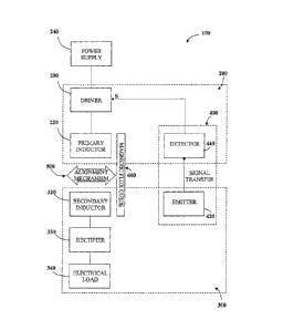
Referring now to Fig. lc, which shows a block diagram representing the main
components of the inductive transfer system 100, various features are included
to improve
power transfer across the inductive couple.
The inductive power outlet 200 includes a primary inductor 220, wired to a
power
supply 240 via a driver 230. The driver 230 typically includes electronic
components, such as a
switching unit for example, for providing an oscillating electrical potential
to the primary
inductor 220. The oscillating electrical potential across the primary inductor
220 produces an
oscillating magnetic field in its vicinity.
The inductive power receiver 300 includes a secondary inductor 320 wired to an
electric load 340, typically via a rectifier 330. The secondary inductor 320
is configured such
that, when placed in the oscillating magnetic field of an active primary
inductor 220, a
secondary voltage is induced across the secondary inductor 320. The secondary
voltage may be
used to power the electric load 340. It is noted that an induced secondary
voltage across the
secondary inductor 320 produces an alternating current (AC). Where the
electric load 340
requires direct current (DC), such as for charging electrochemical cells, the
rectifier 330 is
provided to convert AC to DC.
In contradistinction to prior art inductive power transfer systems, which have
proved
impractical or commercially unviable, embodiments of the current invention
include further
?,5
elements for improving the efficiency of power transfer from the inductive
power outlet 200 to
the inductive power receiver 300. For example, preferred embodiments of the
invention include
a signal transfer system 400, an alignment mechanism 500 and a magnetic flux
guide 600.
The signal transfer system 400 provides a channel for passing signals between
the
inductive power receiver 300 and the inductive power outlet 200. The signal
transfer system
400 includes a signal emitter 420, associated with the inductive power
receiver 300 and a
signal detector 440, associated with the inductive power outlet 200. Signals
may perform a
variety of functions such as inter alia, confirming the presence of a power
receiver 300,
regulating power transfer or for communicating required power transmission
parameters. The
12
CA 02718901 2010-09-17
WO 2009/116025 PCT/1L2008/001641
latter being particularly useful in systems adapted to work at multiple power
levels. Various
signal transfer systems may be used such as optical, inductive, ultrasonic
signal emitters or the
like in combination with appropriate detectors.
The alignment mechanism 500 is provided to facilitate the alignment of the
secondary
inductor 320 with the primary inductor 220 thereby improving the efficiency of
the inductive
transfer system 100. Where the user is able to see the primary inductor 220
directly, the
secondary inductor 320 may be aligned by direct visual observation. However,
where the
primary inductor 220 is concealed behind an opaque surface, alternative
alignment mechanisms
500 may be necessary. Such alignment mechanisms 500 may include tactile,
visual and/or
audible indications, for example.
The magnetic flux guide 600 is provided to guide magnetic flux from the
primary
inductor 220 to the secondary inductor 320 and to prevent flux leakage out of
the inductive
power transfer system 100, particularly into metallic or other conductive
materials in the
vicinity.
Prior art inductive power transfer systems have typically been either
inefficient or
impractical for powering electrical devices wirelessly. As a result, in spite
of the long felt need
to reduce trailing wires, the use of inductive power transfer has been
generally limited to low
power applications such as the charging of batteries. In order to be
practical, an inductive
power transfer system must be efficient, safe and unobtrusive, preferably
having small
?.0
dimensions and being lightweight. As will be described hereinbelow,
embodiments of the
present invention are directed towards providing an inductive power transfer
system which
answers these requirements.
Particular aspects of the current invention include:
= A transmission-guard for preventing the inductive power outlet 200 from
?,5 transmitting power in the absence of an inductive power receiver
300.
= An AC-DC rectifier 330 which uses electronic switches for reducing heat
loss
from diodes.
= An inductive power receiver 300 having a heat dissipation system such
that a
user may comfortably and safely handle the inductive power receiver 300.
10 = A
magnetic flux guide 600 constructed from thin materials and which is adapted
to improve flux linkage between the primary inductor 220 and the secondary
inductor 320 as well as to prevent flux leakage into the surroundings.
13
CA 02718901 2010-09-17
WO 2009/116025 PCT/1L2008/001641
= A driver 230 configured and operable to generate a driving voltage which
oscillates at a transmission frequency which is substantially different from
the
resonant frequency of the inductive couple.
Any one of the abovedescribed aspects by itself represents a significant
improvement to
the prior art. However, it is particularly noted that for any inductive power
transfer system 100
to be practical for powering electrical devices, it needs to incorporate at
least two or more of
the abovedescribed features in combination. More detailed descriptions of
embodiments of the
invention which incorporate these features are given below.
Transmission-Guard
Reference is now made to Fig. 2a which shows a block diagram representing a
transmission-guard 2100 for preventing an inductive power outlet 2200 from
transmitting
power in the absence of a secondary unit 2300 connected to an electric load
2340, according to
another embodiment of the invention.
The inductive power outlet 2200 consists of a primary coil 2220, wired to a
power
supply 2240, for inductively coupling with a secondary coil 2320 wired to an
electric load
2340. The primary coil 2220 is wired to the power supply 2240 via a driver
2230 which
provides the electronics necessary to drive the primary coil 2220. Driving
electronics may
include a switching unit providing a high frequency oscillating voltage
supply, for example.
Where the power outlet 2200 consists of more than one primary coil 2220, the
driver 2230 may
additionally consist of a selector for selecting which primary coil 2220 is to
be driven.
It is a particular feature of this embodiment of the invention that a
transmission-guard
2100 is provided consisting of a transmission-lock 2120 connected in series
between the power
supply 2240 and the primary coil 2220. The transmission-lock 2120 is
configured to prevent
15 the primary coil 2220 from connecting to the power supply 2240
unless it is released by a
transmission-key 2140. The transmission-key 2140 is associated with the
secondary unit 2300
and serves to indicate that the secondary coil 2320 is aligned to the primary
coil 2220.
With reference to Fig. 2b, a schematic representation is shown of an inductive
power
outlet 2200 protected by an exemplary magnetic transmission-guard 2100
according to another
0 embodiment of the present invention. Power may only be provided by
the protected power
outlet 2200 when an authenticated secondary unit 2300 is aligned thereto.
14
CA 02718901 2010-09-17
WO 2009/116025 PCT/1L2008/001641
The protected power outlet 2200 includes a magnetic transmission-lock 2120
consisting
of an array of magnetic switches 2122 electrically connected in series between
the primary coil
2220 and the driver 2230. A magnetic transmission-key 2140 consisting of an
array of
magnetic elements 2142 is provided within the authenticated secondary unit
2300.
The configuration of magnetic elements 2142 in the transmission-key 2140 is
selected
to match the configuration of magnetic switches 2122 in the transmission-lock
2120. The
authenticated secondary unit 2300 may be aligned with the protected induction
outlet 2200 by
aligning both the transmission-key 2140 with the transmission-lock 2120 and
the secondary
coil 2320 with the primary coil 2220. Once correctly aligned, all the magnetic
switches 2122 in
[0 the transmission-lock 2120 are closed and the driver 2230 is thereby
connected to the primary
coil 2220.
Various examples of magnetic switches 2122 are known in the art including for
example reed switches, Hall-effect sensors or such like. Such magnetic
switches 2122 may be
sensitive to any magnetic elements 2142 such as either North or South poles of
permanent
5 magnets or electromagnetic coils for example. It is farther noted that
Hall-effect sensors may
be configured to sense magnetic fields of predetermined strength.
According to certain embodiments, the magnetic transmission-key 2140 may
consist of
a permanent magnet and a ferromagnetic element incorporated with in the
secondary unit 2300.
The characteristics of the magnetic field produced by a transmission-key of
this type depend
:0 upon the strength and position of the permanent magnetic as well as the
dimensions and
characteristics of the ferromagnetic element. The magnetic transmission-lock
2120 may consist
of an array of magnetic switches, such as unipolar Hall switches for example,
which are
strategically placed and orientated such that they connect the primary coil
2220 to the driver
2230 only when triggered by a particular combination of a permanent magnet and
ferromagnetic element.
It is noted that permanent magnets may commonly be provided to assist with
alignment
of the secondary coil 2320 to the primary coil 2220. Ferromagnetic elements
may also be
commonly included in secondary units 2300 for providing flux guidance from the
primary coil
2220 to the secondary coil 2320. The magnetic transmission-lock 2120 may
therefore be made
,0 sensitive to these components. Indeed a single magnetic transmission-
lock 2120 may be
provided which is configured to detect various secondary units and to
selectively connect more
than one primary coil 2220 depending on the secondary unit detected.
CA 02718901 2010-09-17
WO 2009/116025 PCT/1L2008/001641
Referring back to Fig. 2a, according to other embodiments of the transmission-
guard
2100, a power outlet 2200 may be protected by a transmission-lock 2120 which
may be
released when a release signal SR is received by a detector 2124. The release
signal SR may be
actively emitted by the transmission-key 2140 or alternatively the
transmission-key may
passively direct the release signal towards the detector 2124.
One example of a passive transmission-key 2140 is shown in Figs. 2c-e which
represent
an optical transmission-guard 2100 according to a further embodiment of the
invention.
The transmission-guard 2100 consists of an active optical transmission-lock
2120'
incorporated within an inductive power outlet 2200' and a passive optical
transmission-key
2140' incorporated within the secondary unit 2300.
With particular reference to Fig. 2c, the optical transmission-lock 2120'
includes a
switch 2122', an optical detector 2124', such as a photodiode, a
phototransistor, a light
dependent resistor or the like, and an optical emitter 2126' such as light
emitting diode (LED).
The switch 2122' is normally open but is configured to close when a release
signal SR is
received by the optical detector 2124', thereby connecting a primary coil 2220
to a driver 2230.
The optical emitter 2126' is configured to emit the optical release-signal SR
which is not
directly detectable by the optical detector 2124'.
Referring now to Fig. 2d, the optical transmission-key 2140' includes a
bridging
element 2142' such as an optical wave-guide, optical fiber, reflector or the
like. The bridging
?.0 element 2142' is configured to direct the optical release-signal SR
from the optical emitter
2124' towards the optical detector 2126', when a secondary coil 2320 is
aligned with the
primary coil 2220.
When the secondary unit 2300 is correctly aligned with the inductive power
outlet
2200, as shown in Fig. 2e, the secondary coil 2320 aligns with the primary
coil 2220' and the
15 passive optical transmission-key 2140' aligns with the optical
transmission-lock 2120'. The
optical release-signal SR is thus detected by the optical detector 2126' and
the switch 2122' is
closed connecting the primary coil 2220 to the driver 2230.
It is noted that many materials are partially translucent to infra-red light.
It has been
found that relatively low intensity infra red signals from LEDs and the like,
penetrate several
10 hundred microns of common materials such as plastic, cardboard, Formica
or paper sheet, to a
sufficient degree that an optical detector 2124', such as a photodiode, a
phototransistor, a light
dependent resistor or the like, behind a sheet of from 0.1 mm to 2 mm of such
materials, can
receive and process the signal. For example a signal from an Avago HSDL-4420
LED
16
CA 02718901 2010-09-17
WO 2009/116025 PCT/1L2008/001641
transmitting at 850mn over 24 degrees, may be detected by an Everlight PD15-
22C-TR8 NPN
photodiode, from behind a 0.8 mm Formica sheet. For signaling purposes, a high
degree of
attenuation may be tolerated, and penetration of only a small fraction, say
0.1% of the
transmitted signal intensity may be sufficient.
Although an optical transmission-key 2140' is described above, it will be
appreciated
that other passive transmission-keys may incorporate bridging elements
configured to guide
release-signals of other types. For example, a ferromagnetic bridge may be
incorporated for
transmitting magnetic release-signal from a magnetic element to a magnetic
detector such as a
Hall-effect sensor or the like. The magnetic emitter in such a case may be the
primary coil
itself.
Alternatively, audio signals may be guided through dense elements, or low
power
microwaves along microwave wave guides for example.
An example of an active optical transmission-key 2140" is shown in Fig. 2f
representing a transmission-guard 2100" according to another embodiment of the
invention.
The transmission-guard 2100" of this embodiment includes a transmission-lock
2120"
incorporated within an inductive power outlet 2200 and an active optical
transmission-key
2140" incorporated within secondary unit 2300.
The active optical transmission-key 2140" includes an optical emitter 2142",
configured to emit an optical release-signal SR, and the transmission-lock
2120" includes a
switch 2122" and an optical detector 2124". The transmission-lock 2120" is
configured to close
the switch 2122" thereby connecting a primary coil 2220 to a driver 2230 when
the optical
detector 2124" receives the release-signal S.
When the secondary unit 2300 is aligned with the inductive power outlet 2200,
the
transmission-key 2140" emits an optical release-signal SR which is received by
the optical
?,5
detector 2124" of the transmission-lock 2120" and this closes the switch
2122". Thus the
inductive power outlet 2200" is enabled to transfer power to the secondary
coil 2320.
It will be appreciated that a release signal SR may be coded to provide a
unique
identifier. Coding may be by modulation of frequency, pulse frequency,
amplitude or the like.
The code may be used, for example, to identify the type or identity of the
secondary unit for
;0
authentication. Other data may additionally be encoded into the release-
signal. This data may
include required power transmission parameters, billing information or other
information
associated with the use of the power outlet.
17
CA 02718901 2010-09-17
WO 2009/116025 PCT/1L2008/001641
Although an optical active transmission-key 2140" is described above, it will
be
appreciated that other active transmission-keys may emit other types of
release-signals. For
example, the secondary coil 2320 may be used to transmit a magnetic release-
signal to a
magnetic detector incorporated in the transmission-lock. This could be a Hall-
effect sensor or
the like or even the primary coil 2220 itself.
To actively emit a release-signal transmission-keys typically require a power
source. In
some cases, particularly where the secondary unit is incorporated into a
portable electrical
device, power may be provided by internal power cells with the secondary unit.
Alternatively,
power may be drawn from a power pulse transferred from the primary coil to the
secondary
coil.
In certain embodiments of the invention, the inductive power outlet transfers
a periodic
low energy power pulse, for example a pulse of a few milliseconds duration may
be transmitted
by the primary coil at a frequency of 1 hertz or so. When a secondary coil is
brought into the
vicinity of the primary coil the power may be transferred to the secondary
coil and may be used
to power an active transmission-key.
In other embodiments of the transmission-guard, a first transmission-lock
(preferably a
passive transmission-lock) associated with the secondary unit, releases a
first transmission-lock
thereby indicating the probable presence of a secondary coil. A low energy
power pulse is then
emitted by the primary coil to power an active second transmission-key which
may release a
?.0 second transmission-lock thereby connecting the primary coil to a
driver.
Synchronous Rectifier
Reference is now made to Fig. 3a showing a circuit diagram of a typical full-
wave
rectifier 3100 of the prior art. The rectifier has two input terminals T1 and
T2 and two output
l5 terminals T3 and T4. When an alternating current source ACin is wired to
the two input
terminals T1 and T2, a direct current output DCout may be drawn from the two
output terminals
T3 and T4 of the rectifier 3100.
Four diodes D1_4 are arranged so that two diodes D1 and D2 form a first branch
3110 of
a Graetz circuit and the other two diodes D3 and D4 form a second branch 3120
of the Graetz
,0 circuit. The anodes of two upstream diodes DI and D3 are wired to the
first output terminal T3
and the cathodes of the two downstream diodes D2 and D4 are wired to the
second output
terminal T4. The cathode of the first upstream diode Di and the anode of first
downstream
18
CA 02718901 2010-09-17
WO 2009/116025 PCT/1L2008/001641
diode D2 are wired to the first input terminal T1 and the cathode of the
second upstream diode
D3 and the anode of second downstream diode D4 are wired to the second input
terminal T2.
When the polarity of the first input terminal T1 is positive relative to the
second input
terminal T2, current flows through the first downstream diode D2 and through
the second
upstream diode D3, When the polarity of the first input terminal T1 is
negative relative to the
second input terminal T2, current flows through the second downstream diode D4
and through
the first upstream diode D1.
Diode bridge rectifiers, such as that shown in Fig. 3a, are used to produce an
output
with a fixed polarity that is independent of the polarity of the input. Such
diode bridge
rectifiers may be used in AC-to-DC power converters, for example. Optionally,
the output is
smoothed by a smoothing capacitor C.
It will be appreciated that power is lost from each diode with each reversal
of polarity.
In high frequency power converters, where the polarity of the input terminals
Ti and T2 may
oscillate at a frequencies of 100 kHz or more, such power losses may result in
significant
[5 heating of the bridge circuit and its surrounding components, which may
result in reduced
reliability or failure.
Power loss may be reduced by replacing diodes with electronic switches, such
as the
Power MOSFETs shown in Fig. 3a, which have much lower associated power loss.
Fig. 4a is a
block diagram of one such synchronous full-wave rectifier 4200 in which the
first downstream
!O diode D2 and the second downstream diode D4 of the diode bridge of Fig.
3a have been
replaced by two electronic switches M2 and M4.
The electronic switches M2 and M4 are controlled by switching signals 02 and
G4 which
switch them between the ON and OFF states. The switching signal 02 controlling
the
electronic switch M2 must be synchronized to switch to the ON state whenever
the polarity of
the first input terminal T1 is positive relative to the second input terminal
T2. The switching
signal G4 controlling the electronic switch M4 must be synchronized to switch
to the ON state
whenever polarity of the first input terminal T1 is negative relative to the
second input terminal
T2.
Typically, this synchronization is achieved by drawing the first switching
signal G2
0 from the voltage of the second input terminal T2 and drawing the second
switching signal G4
from the voltage of the first input terminal Ti.
The above described synchronous full-wave rectifier 4200 in which two diodes
are
replaced by MOSFETs may reduce power loss from the rectifier by up to 50% as
compared
19
CA 02718901 2010-09-17
WO 2009/116025 PCT/1L2008/001641
with the diode bridge rectifier 4100 of the prior art. Where further reduction
in power loss is
required it would be desirable to replace the remaining two diodes DI and D3
with electronic
switches. However, it is much more difficult to synchronize four electronic
switches without
inadvertently causing short circuits between either the input or output
terminals.
Fig. 4b is a block diagram of a second synchronous full-wave rectifier 4300 in
which all
four diodes D1-4 of the diode bridge of Fig. 3a have been replaced by
electronic switches M1-4.
In order to provide an output DCout of constant polarity, the switching
signals 014 need to be
carefully controlled.
When the polarity of the first input terminal T1 is positive relative to the
polarity of the
second input T2, the first upstream and second downstream electronic switches
M1 and M4
must be switched to the OFF state and the first downstream and second upstream
electronic
switches M2 and M3 must be switched to the ON state. When the polarity of the
first input
terminal T1 is negative relative to the polarity of the second input terminal
12, the first
upstream and second downstream electronic switches M1 and M4 must be switched
to the ON
state and the electronic switches first downstream and second upstream
electronic M2 and M3
must be switched to the OFF state.
Synchronization of the switching signals G1-4, is complicated by an additional
constraint. In order to prevent shorting across the output terminals, the
upstream and
downstream electronic switches along a common branch 4310, 4320 must never be
in the ON
?,0 state
at the same time. In practice, when both of the switching signals G1 and 02
controlling the
two electronic switches M1 and M2 along the first branch 4310 are each drawn
from one of the
input terminals T1 and 12, the two switches Mi and M2 are periodically both in
their ON states.
Because the switches M1 and M2 are adjacent along the first branch 4310 of the
circuit, a short
circuit is formed between the output terminals T3 and 14. Similar shorting may
occur along the
?5 second
branch 4320 when the switching signals 03 and G4 which control the other two
electronic switches M3 and M4 are each drawn from one of the input terminals
T1 and 12.
According to preferred embodiments of the invention, only the switching
signals G2
and G4 for the downstream electronic switches M2 and M4 are drawn directly
from the voltage
at the input terminals T1 and T2 whilst the switching signals G1 and 03 for
the upstream
switches M1 and M3 are controlled independently. Preferably, the switching
signals G1 and 03
are responsive to changes in the cathode current of switches M1 and M3
respectively.
Fig. 4c shows an exemplary current-triggered synchro-rectifier 4330, which may
serve
as an electronic switch M incorporated into a bridge synchro-rectifier 4300.
The current-
CA 02718901 2010-09-17
WO 2009/116025 PCT/1L2008/001641
triggered synchro-rectifier 4330 includes a Power MOSFET 4130, such as that
shown in Fig.
3b, and a current monitor 4332. The current monitor 4332 is wired to the drain
terminal 4136
of the Power MOSFET 4130 and is configured to send a current-based gate signal
Gi to the
gate terminal 4138 of the Power MOSFET when the drain-current Id exceeds a
predetermined
threshold Ith. Although in the above example the current-triggered synchro-
rectifier 4330
includes an n-channel MOSFET 4130, it will be appreciated that in other
embodiments current-
triggered synchro-rectifiers may incorporate p-channel MOSFETs.
In order to understand the functioning of the current-triggered synchro-
rectifier 4330
consider the case where a sinusoidal alternating voltage is connected across
the cathode 4334 '
and the anode 4336 terminals of the current-triggered synchro-rectifier 4330.
Fig. 4d shows
three graphs showing variations in 1) the voltage drop Vd from the cathode
4334 to the anode
4336, 2) the drain-current Id, and 3) the MOSFET state during one voltage
cycle.
= For the first half of the sinusoidal cycle the voltage drop Vd between
the cathode 4334 and
the anode 4336 is negative, thus the polarity of the cathode 4334 is negative
relative to the
anode 4336. Consequently, no current flows through the drain-terminal 4136 and
the
MOSFET remains in the OFF state.
= At the beginning of the second half of the sinusoidal cycle, the voltage
drop Vd between the
cathode 4334 and the anode 4336 increases above zero. The polarity of the
cathode 4334
becomes positive relative to the anode. 4336 so a small drain-current Id
begins to flow
through the diode 4132. This current is measured by the current monitor 4332.
= During the third quarter of the cycle, the voltage drop Vd between the
cathode 4334 and the
anode 4336 continues to rise. The current monitor 4332 measures an increasing
drain-
current Id.
= When the drain-current Id exceeds the predetermined threshold Ith, the
current-based gate
signal Gi triggers the MOSFET 4130 to switch to the ON state.
= As long as the MOSFET 4130 is in the ON state, current flows through the
ohmic
conductive path of the electronic switch 4131. Consequently, the drain-current
Id varies in
proportion to the voltage drop Vd.
= During the last quarter of the cycle, the voltage drop Vd between the
cathode 4334 and the
anode 4336 decreases. The current monitor 4332 measures a decreasing drain-
current Id.
= When the drain-current falls below the predetermined threshold Ith, the
current-based gate
signal Gi triggers the MOSFET 4130 to switch to the OFF state.
21
CA 02718901 2010-09-17
WO 2009/116025 PCT/1L2008/001641
Fig. 4e is a circuit diagram representing a synchronous full-wave bridge
rectifier 4400
incorporated within an inductive power receiver according to a further
embodiment of the
invention. The electronic switches M1_4 are all MOSFET transformers having
three terminals: a
source terminal, a drain terminal and a gate terminal. The upstream MOSFETs M1
and M3 are
both n-channel MOSFETs and their source terminals are both wired to the first
output terminal
T3 of the rectifier. The downstream MOSFETs M2 and M4 are both p-channel
MOSFETs and
their source terminals are both wired to the second output terminal T4 of the
rectifier. The drain
terminals of the first upstream MOSFET M1 and the first downstream MOSFET M2
are both
wired to the first input terminal T1 of the rectifier and the drain terminals
of the second
upstream MOSFET M3 and the second downstream MOSFET M4 are both wired to the
second
input terminal T3 of the rectifier.
The input terminals T1 and T2 are wired to a secondary coil L2 of a power
transformer
which is inductively coupled to a primary coil (not shown). The secondary coil
L2 provides an
alternating current input to the two input terminals T1 and T2.
The gate terminals of the downstream MOSFETs M2 and M4 are wired to the input
terminals T2 and T1 via smoothing circuits 4420, 4440 respectively. The
switching signals G2
and 04, are therefore in out of phase with each other.
The gate terminals of the upstream MOSFETs M1 and M3 receive switching signals
Gi
and 03 driven by their own drain-currents Idi and Id3. The drain current 'dl
of the first upstream
MOSFET Mi is monitored by a first current transformer 4410, in which a primary
current
monitor coil CTip transfers the current signal to a secondary current monitor
CT25 the output of
which is rectified and relayed to a first input IN1 of a driver 4450 which
amplifies the signal
before outputing a signal from a first output OUTi. This first output signal
from the driver is
then fed back to the first upstream MOSFET M1 such that when the drain current
'dl exceeds a
threshold value the MOSFET M1 switches itself to the ON state. This produces a
switching
signal G1 at the same frequency as the alternating current input ACm=
Similarly the drain current Id3 of the second upstream MOSFET M2 is monitored
by a
second current transformer 4430, in which a primary current monitor coil CT2p
transfers the
current signal to a secondary current monitor CT25 the output of which is
rectified and relayed
0 to a
second input IN2 of the driver 4450 which amplifies the signal before
outputing a signal
from a second output OUT2. The second output signal from the driver is then
fed back to the
second upstream MOSFET M3 such that when the drain current Id2 exceeds a
threshold value
22
CA 02718901 2010-09-17
WO 2009/116025 PCT/1L2008/001641
the MOSFET M3 switches itself to the ON state. This produces a switching
signal G3 at the
same frequency as the alternating current input ACin=
Although in the example hereabove, current transformers 4410, 4430 are used to
monitor the drain-currents fd2, in alternative embodiments other current
monitors such as
ammeters, galvanometers, Hall effect sensors or the like may be preferred.
Heat Dissipation within Inductive Power Receivers
Reference is now made to Fig. 5a showing a laptop computer 5300 drawing power
from
an inductive power outlet 5200 via an inductive power adapter 5100, according
to a further
embodiment of the present invention. The adaptor is configured such that it
can be safely
handled by a user while it is operation.
The power adapter 5100 includes an inductive receiver 5120, housed in a casing
5160
and a power connector 5140 for connecting to an electrical device, such as the
computer 5300.
The inductive receiver 5120 includes a secondary inductor 5122 configured to
couple with a
primary inductor 5220 in the power outlet 5200. Typically, the primary
inductor 5220 is wired
to a power source 5240 via a driver 5230. The driver 5230 provides an
oscillating driving
voltage to the primary inductive coil 5220.
Preferably, an alignment mechanism (not shown) is provided for aligning the
secondary
inductor 5122 to the primary core 5220. The alignment mechanism may consist of
a primary
?,0 magnetic element in the inductive outlet configured to snag and/or
engage a secondary
magnetic element in the power adaptor 5100.
It will be appreciated that electrical components of power converters generate
heat.
There are a number of problems associated with the heat generated in an
inductive receiver
5120, particularly in systems running at high power above say 50W or 100W.
Heat produces
?.5 high temperatures which can reduce overall efficiency and may also
reduce the reliability of
components. Much design effort is typically required to overcome this problem,
and other
factors such as the dimensions of the system may be compromised as a result.
In practice, electrical components of the power adapter 5100 are selected
which
function at high temperatures. However, the maximum temperature of the casing
5160 is
;0 further constrained by the requirement that it is to be handled by the
user. If the casing 5160
reaches high temperatures, above 50 degrees Celsius or so, a user may find
handling the
adapter to be unpleasant and may even be at risk of injury. In order to allow
a user to
comfortably and safely handle the adaptor 5100, it is a particular feature of
the present
invention that a heat dissipation system for directing heat away from the hand
grip 5162.
23
CA 2718901 2017-03-13
W0200/116025 CA2718901 125-29
CA/PCT
The heat dissipation system may be better understood with reference to Figs.
5b-c
showing an exemplary inductive power adapter 5100 according to another
embodiment of
the invention. Fig. 5b shows an isometric projection and Fig. 5c shows an
exploded view
of the same embodiment of the power adaptor 5100.
The exemplary power adapter 5100 includes an inductive receiver 5120, and a
heat sink
5130 housed between a lower casing 5160L, and an upper casing 5160U and a
power
connector 5140 which can be wound around a hand grip 5162 for storage.
The inductive power receiver 5120 consists of a secondary inductive coil 5122
a
ferromagnetic disk 5124 and a printed circuit board (PCB) 5126. The heat sink
5130 of the
exemplary embodiment consists of a metallic disk sandwiched between the
inductive receiver
5120 and the upper casing 5160U. The ferromagnetic disk 5124 may serve as a
flux guiding
core to improve inductive coupling between the secondary inductive coil 5122
and a primary
inductive coil 5220 (Fig. 1) of an inductive power outlet 5200.
When the power adapter 5100 is in operation, heat is generated by a number of
components of the inductive receiver 5120. An alternating current is induced
in the secondary
inductive coil 5122 therefore causing the coil wire to heat up. Furthermore
hot spots are
typically generated around certain electrical components typically provided on
the PCB 5126,
such as rectifiers, diodes, MOSFETS, power regulators, LD0s, feedback
transmitters or the
like.
The heat sink 5130 is typically a thermal conductive material such as
aluminum, copper
or the like which serves to distribute heat more evenly around the inductive
receiver 5120.
Preferably, thermal vias are provided through the PCB 5126 and thermal grease
or a similar
agent is used to improve thermal contact between the heat sink 5130, PCB 5126,
ferromagnetic
disk 5124 and secondary coil 5122.
Air outlets 5132 are provided in the top 5161 of the upper casing 5160U
allowing hot
air from inside the power adaptor to escape into the atmosphere. Air inlets
5134 are provided in
the bottom 5165 and sides 5167 of the lower casing 5160L and on the sides 5163
of the upper
casing 5160U allowing cool air to enter into the power adaptor from below. It
is a particular
feature of the exemplary embodiment that the outer diameter d of the heat sink
is smaller the
10 inner
diameter D of the casing 5160 thus allowing air to circulate around the
inductive receiver
5120. Thus hot air heated by the inductive power receiver 5120 flows out of
the adapter 5100
through the outlets 5132 and cool air from outside is drawn into the adapter
5100 through said
air inlets 5134. The hand grip 5162 may be additionally protected from heat by
a barrier of
thermal insulating material.
24
WO 2009/116025 CA2718901 125-29 CA/PCT
It is noted that the air outlets 5132 may allow dust to enter the power
adapter 5100. In
some embodiments therefore a dust-guard is provided to prevent dust from
entering the outlets
5132. In the exemplary embodiment, the grip 5162 overhangs the outlets 5132
serving as a dust-
guard to prevent dust from entering the adapter 5100 whilst in operation. When
not in operation,
the power connector 5140 may be wound around the hand grip 5162, thereby
providing further
protection against dust.
In certain embodiments, the PCB 5126 includes a light emitting diode (not
shown) used
as a feedback transmitter for sending signals to an optical detector in the
power outlet 5200 (Fig.
5a). It will be appreciated that in such embodiments, it is necessary that a
clear line-of- sight is
maintained between the optical emitter and detector. To this end, in preferred
embodiments an
optical window, transparent to the wavelength of the wavelength of the optical
transmission, is
provided through the secondary inductive coil 5122, ferrite disk 5124, lower
casing 5160L and
other layers between the PCB 5126 and the primary coil 5220 (Fig. 5a).
Magnetic Flux Guidance
Referring now to Figs. 5d and 5e, an inductive power receiver 5200 is shown
including a
secondary inductor 5220, a magnetic flux guide 5260 and a PCB 5270, according
to a further
embodiment of the invention. The secondary inductor 5220 is configured to
receive power
inductively from a primary inductor of an inductive power outlet (not shown).
The magnetic flux
guide 5260 is provided to direct magnetic flux from the primary inductor to
the secondary
inductor 5220 and to reduce flux leakage to the surroundings. The magnetic
flux guide 5260
consists of a ferromagnetic core 5262 and a magnetic shield 5264. The
ferromagnetic core 5262
is provided to guide magnetic flux from an active primary inductor to the
secondary inductor
5220.
In preferred embodiments, the ferromagnetic core 5262 is constructed from
amorphous
ferromagnetic material, typically cut into wafers from a sheet approximately
20 microns thick or
so. In one exemplary embodiment, the ferromagnetic core consists of two
amorphous
ferromagnetic wafers 5262a, 5262b. A first wafer 5262a is adhered to the
primary inductor 5220
by a first adhesive insulating layer 5265a. A second wafer 5262b is adhered to
the first wafer
5262a by a second adhesive insulating layer 5265b. The two wafers 5262a, 5262b
serve as a
ferromagnetic core guiding magnetic flux from a primary inductor to the
secondary inductor
5220. It is a particular feature of preferred embodiments that the
ferromagnetic wafers 5262a,
5262b each have a radial slit 5263a, 5263b to prevent the buildup of eddy
currents within the
wafer due to the oscillating magnetic field produced by the primary inductor.
Where
CA 2718901 2018-01-29
CA 02718901 2010-09-17
WO 2009/116025 PCT/1L2008/001641
the wafer has a circular cross section, the slit may extend inwardly
diametrically from the
circumference.
The magnetic shield 5264 is provided to prevent flux leakage into the
surroundings.
Preferably, the magnetic shield 5264 is also fabricated from a sheet of thin
amorphous
ferromagnetic material and may be adhered to the PCB by a third adhesive
insulating layer
5265c.
It will be appreciated that a magnetic shield is of particular importance when
the
inductive receiver 5200 is mounted upon a conductive surface or a device
containing
conductive components. Thus, for example, when such an inductive power
receiver 5200 is
mounted upon an electrical device, such as a computer, mobile telephone or the
like, the
magnetic shield 5264 prevents magnetic flux from leaking into the metallic
components of the
electrical device and causing them to heat up.
Amorphous ferromagnetic sheets may have a thickness of around 20 microns. When
laminated by a polymer laminate on both sides the overall thickness of the
sheet is around 60
microns. Thus, in contradistinction to other ferrite elements used to guide
magnetic flux in
inductive systems, amorphous ferromagnetic materials may be used to fabricate
an extremely
thin magnetic guide 5260. A thin magnetic guide 5260 in turn allows the
inductive power
receiver 5200 to be flexible and unobtrusive. It will be appreciated that
these considerations are
very important in the design and manufacture of device mounted inductive
receivers. Various
10 methods of fabricating magnetic guiding elements from amorphous
ferromagnetic material
include, inter alia: printing, stamping, cutting, amorphous ferromagnetic
microwire cloth and
the like.
Power Transmission at a Non-resonant Frequency
15 The strength of an induced voltage in the secondary inductor of an
inductive couple
varies according to the oscillating frequency of the electrical potential
provided to the primary
inductor. The induced voltage is strongest when the oscillating frequency
equals the resonant
frequency of the system. The resonant frequency fR depends upon the inductance
L and the
1
capacitance C of the system according to the equation Az =
27z-V-LC =
0 Known inductive power transfer systems typically transmit power at
the resonant
frequency of the inductive coupling. This can be difficult to maintain as the
resonant frequency
26
CA 02718901 2010-09-17
WO 2009/116025 PCT/1L2008/001641
of the system may fluctuate during power transmission, for example in response
to changing
environmental conditions or variations in alignment between primary and
secondary coils.
Inductive transfer systems designed to transmit at resonance therefore require
tuning
mechanisms for maintaining transmission at the resonant frequency of the
system. Tuning may
be achieved by adjusting the driving frequency to seek resonance. For example,
United States
Patent No. 6,825,620, titled "Inductively coupled ballast circuit" to Kuennen
et al. describes a
resonance seeking ballast circuit for inductively providing power to a load.
The ballast circuit
includes an oscillator, a driver, a switching circuit, a resonant tank circuit
and a current sensing
circuit. The current sensing circuit provides a current feedback signal to the
oscillator that is
representative of the current in the resonant tank circuit. The current
feedback signal drives the
frequency of the ballast circuit causing the ballast circuit to seek
resonance. The ballast circuit
preferably includes a current limit circuit that is inductively coupled to the
resonant tank
circuit. The current limit circuit disables the ballast circuit when the
current in the ballast
circuit exceeds a predetermined threshold or falls outside a predetermined
range.
Alternatively, tuning may be achieved by adjusting the characteristics of the
inductive
system. For example, United States Patent No. 7,212,414, titled "Adaptive
inductive power
supply" to Bauman describes a contactless power supply which has a dynamically
configurable tank circuit powered by an inverter. The contactless power supply
is inductively
coupled to one or more loads. The inverter is connected to a DC power source.
When loads are
added or removed from the system, the contactless power supply is capable of
modifying the
resonant frequency of the tank circuit, the inverter frequency, the inverter
duty cycle or the rail
voltage of the DC power source.
Tuning mechanisms such as those described above are necessary in order to
maintain
transmission at resonance because resonant transmission is highly sensitive.
At resonance small
).,5 variations to the system result in large changes to the power
transferred. A further problem
associated with resonant transmission is the high transmission voltages
involved. At high
operating voltages, the capacitors and transistors in the circuit need to be
relatively large.
Reference is now made to Fig. 6a showing a block diagram of the main elements
of an
inductive power transfer system 6100 adapted to transmit power at a non-
resonant frequency.
,0 The inductive power transfer system 6100 consists of an inductive power
outlet 6200
configured to provide power to a remote secondary unit 6300 according to
another embodiment
of the invention. The inductive power outlet 6200 includes a primary inductive
coil 6220 wired
27
CA 02718901 2010-09-17
WO 2009/116025 PCT/1L2008/001641
to a power source 6240 via a driver 6230. The driver 6230 is configured to
provide an
oscillating driving voltage to the primary inductive coil 6220.
The secondary unit 6300 includes a secondary inductive coil 6320, wired to an
electric
load 6340, which is inductively coupled to the primary inductive coil 6220.
The electric load
6340 draws power from the power source 6240. A communication channel 6120 may
be
provided between a transmitter 6122 associated with the secondary unit 6300
and a receiver
6124 associated with the inductive power outlet 6200. The communication
channel 6120 may
provide feedback signals S and the like to the driver 6230.
In some embodiments, a voltage peak detector 6140 is provided to detect large
increases in the transmission voltage. As will be descried below the peak
detector 6140 may be
used to detect the removal of the secondary unit 6200, the introduction of
power drains, short
circuits or the like.
Fig. 6b is a graph showing how the amplitude of the operational voltage varies
according to the transmission frequency. It is noted that the voltage is at
its highest when the
transmission frequency is equal to the resonant frequency fR of the system,
this maximum
amplitude is known as the resonance peak 2. It is further noted that the slope
of the graph is
steepest in the regions 4a, 4b to either side of the resonance peak 2. Thus in
inductive transfer
systems, which operate at or around resonance, a small variation in frequency
results in a large
change in induced voltage. Similarly, a small change in the resonant frequency
of the system
results in a large change in the induced voltage. For this reason prior art
inductive transfer
systems are typically very sensitive to small fluctuations in enviromnental
conditions or
variations in alignment between the induction coils.
It is a particular feature of embodiments of the current invention that the
driver 6230
(Fig. 6a) is configured and operable to transmit a driving voltage which
oscillates at a
transmission frequency which is substantially different from the resonant
frequency of the
inductive couple. Preferably the transmission frequency is selected to lie
within one of the
near-linear regions 6, 8 where the slope of the frequency-amplitude graph is
less steep.
One advantage of this embodiment of the present invention may be demonstrated
with
reference now to Fig. 6e. A schematic diagram is shown representing a laptop
computer 6340
W drawing power from an inductive power outlet 6200 via a secondary power
receiving unit
6300. The power receiving unit 6300 includes a secondary inductive coil 6320
which is aligned
to a primary inductive coil 6220 in the inductive power outlet 6200. Any
lateral displacement
of the secondary power receiving unit 6300 changes the alignment between the
secondary
inductive coil 6320 to the primary inductive coil 6220. As a result of the
changing alignment,
28
CA 02718901 2010-09-17
WO 2009/116025 PCT/1L2008/001641
the combined inductance of the coil pair changes which in turn changes the
resonant frequency
of the system.
If the inductive power outlet 6200 transmits power at the resonant frequency
of the
system, even a small lateral movement would reduce significantly the amplitude
of the induced
voltage. In contradistinction, according to embodiments of the present
invention, the inductive
power outlet 6200 transmits power at a frequency in one of the regions 6, 8 to
either side of the
resonance peak 2 (Fig. 6b) where the slope of the resonance graph is much
shallower.
Consequently, the system has a much larger tolerance of variations such as
lateral movement.
Another advantage of non-resonant transmission is that the transmission
frequency may
be used to regulate power transfer. In known inductive power transfer systems,
power is
typically regulated by altering the duty cycle of the transmission voltage
provided by the
driver. Thus, it will be appreciated that when the transmission frequency is
not equal to the
resonance frequency of the system, the driver 6230 may be configured to adjust
the
transmission frequency in order to regulate the power transfer.
Referring back to Fig. 6b, the frequency of transmission is selected to be in
the
approximately linear region 8 of the curve between a lower frequency value of
f. and an upper
frequency value of fu. A transmission frequency ft, higher than the resonant
frequency fR of the
system, produces an induced voltage of V. The induced voltage can be increased
by reducing
the transmission frequency and can be reduced by increasing the transmission
frequency. For
example, an increase in transmission frequency of 8f produces a decrease in
induced voltage of
V.
In some embodiments, a communication channel 6120 (Fig. 6a) is provided
between
the secondary unit 6300 and the inductive power outlet 6200. Such a
communication channel
6120, may be used to communicate required operating parameters which, for
example, may
2, 5 indicate the transmission frequency required by the electric load 6340
to the driver 6230.
Various transmitters 6122 and receivers 6124 may be used with the
communication
channel 6120. Where, as is often the case for inductive systems, the primary
and secondary
coils 6220, 6320 are galvanically isolated for example, optocouplers may have
a light emitting
diode serving as a transmitter which sends encoded optical signals over short
distances to a
K) photo-transistor which serves as a receiver. Optocouplers typically need
to be aligned such that
there is a line-of-sight between transmitter and receiver. In systems where
alignment between
the transmitter and receiver may be difficult to achieve, optocoupling may be
inappropriate and
alternative systems may be preferred such as ultrasonic signals transmitted by
piezoelectric
29
CA 02718901 2010-09-17
WO 2009/116025 PCT/1L2008/001641
elements or radio signals such as Bluetooth, WiFi and the like. Alternatively
the primary and
secondary coils 6220, 6320 may themselves serve as the transmitter 6122 and
receiver 6124.
In certain embodiments, an optical transmitter, such as a light emitting diode
(LED) for
example, is incorporated within the secondary unit 6300 and is configured and
operable to
transmit electromagnetic radiation of a type and intensity capable of
penetrating the casings of
both the secondary unit 6300, and the power outlet 6200. An optical receiver,
such as a
photo diode, a phototransistor, a light dependent resistors of the like, is
incorporated within the
power outlet 6200 for receiving the electromagnetic radiation.
The communication channel 6120 may farther provide a feedback signal during
power
transmission. The feedback transmission may communicate required or monitored
operating
parameters of the electric load 6240 such as:
= required operating voltage, current, temperature or power for the
electric load
6240,
= the measured voltage, current, temperature or power supplied to the
electric load
6240 during operation,
= the measured voltage, current, temperature or power received by the
electric
load 6240 during operation and the like.
In some embodiments, a microcontroller in the driver 6230 may use such
feedback
parameters to calculate the required transmission frequency and to adjust the
driver
?,0 accordingly. Alternatively, simple feedback signals may be provided
indicating whether more
or less power is required.
One example of a power regulation method using simple feedback signals is
shown in
the flowchart of Fig. 6d. The method involves the following steps:
(a) The driver 6230 provides an oscillating voltage at a transmission
frequency ft which
15 is higher than the resonant frequency fR of the system.
(b) A secondary voltage is induced in the secondary coil 6320.
(c) A power monitor in the secondary unit 6300, monitors the power received by
the
electric load 6340.
(d) If the power received by the electric load 6340 lies within a
predetermined range
then no action is taken. If the power received by the electric load E340 is
below the
predetermined range, then a feedback signal of a first type Sa is sent to the
driver. If
the power received by the electric load 6340 is above the predetermined range,
then
a feedback signal of a second type Sb is sent to the driver.
CA 02718901 2010-09-17
WO 2009/116025 PCT/1L2008/001641
(e) A feedback signal is received by the driver 6230.
(f) If the received feedback signal is of the first type Sa, then the
transmission frequency
is increased by an incremental value +6f1. If the received feedback signal is
of the
second type Sb, then the transmission frequency is decreased by an incremental
value -5f2.
It is noted that by using the power regulation method described above, when
the power
received by the load is too high, a series of feedback signals of the first
type Sa will be
transmitted until the power is reduced into the acceptable range. Likewise
when the power
received by the load is too low, a series of feedback signals of the second
type Sb will be
transmitted until the power is increased into the acceptable range. It is
noted that the positive
incremental value 6f1 may be greater than, less than or equal to the negative
incremental value
8f2.
Alternatively, other power regulation methods using frequency adjustment may
be
used. For example, in alternative embodiments, the operating parameters of the
electric load
may be monitored and their values may be transmitted to the power outlet via
the
communications channel 6120. A processor in the power outlet may then
calculate the required
transmission frequency directly.
The method described hereabove, refers to a non-resonant transmission
frequency lying
within the linear region 8 (Fig. 6b), higher than the resonant peak 2. It will
be appreciated
however that in alternative embodiments frequency controlled power regulation
may be
achieved when the transmission frequency lies in the lower linear region 6 of
the resonance
curve. Nevertheless, as explained below, for certain embodiments, the
selection of transmission
frequencies in the higher linear 8 may be preferred.
As described above, the resonant frequency fR of an inductive couple is given
by the
1
15 _____________ formula fR = , where L is the inductance of the system and
C is the capacitance of the
27r-aC
system. Thus any decrease in either the inductance L or the capacitance C of
the system
thereby increases its resonant frequency.
In inductive power outlets transmitting at frequencies above the normal
resonant
frequency of the system, an increase in resonant frequency of the system
causes a large
,0 increase in the transmission voltage. In preferred embodiments, a peak
detector 6140 (Fig. 1) is
be provided to monitor the transmission voltage of the power outlet 6200 and
is configured to
detect large increases in the transmission voltage indicating an increase in
resonant frequency.
31
CA 02718901 2010-09-17
WO 2009/116025 PCT/1L2008/001641
Such increases in transmission voltage may be indicative of power drains,
short circuits,
removal of the secondary unit or the like.
As an example of the use of a peak detector reference is again made to Fig.
6c. It will
be appreciated that in a desktop environment, conductive bodies such as a
paper clip, metal
rule, the metal casing a stapler, a hole-punch or any metallic objects may be
introduced
between the inductive power outlet 6200 and the secondary power receiving unit
6300. The
oscillating magnetic field produced by the primary coil 6220 would then
produce eddy currents
in the conductive body heating it and thereby draining power from the primary
coil 6220. Such
a power drain may be wasteful and/or dangerous.
Power drains such as described above reduce the inductance L of the system.
The
inductance L may also be reduced by the removal of the secondary coil 6220, a
short circuit or
the like. A peak detector 6140, wired to the inductive power outlet, would
detect any of these
scenarios as a large increase in transmission voltage. Preferably, the power
transfer system may
be further configured to shut down, issue a warning or otherwise protect the
user and the
system in the event that the peak detector 6140 detects such an increase in
transmission
voltage.
Fig. 6e is a circuit diagram of an inductive power outlet 6200 and a secondary
unit
6300. The secondary unit 6300 comprises a secondary coil 6320 wired to an
electric load 6340
via a rectifier 6330.
The inductive power outlet 6200 comprises a primary coil 6220 driven by a half-
bridge
converter 6230 connected to a power source 6240. The half-bridge converter
6230 is
configured to drive the primary coil 6220 at a frequency higher than the
resonant frequency of
the system and a peak detector 6140 is configured to detect increases in the
transmission
voltage.
Although only a half-bridge converter is represented in Fig. E6, it is noted
that other
possible driving circuits include: a DC-to-DC converter, an AC-to-DC
converter, an AC-to-AC
converter, a flyback transformer, a full-bridge converter, a flyback converter
or a forward
converter for example.
Thus, by using a transmission voltage oscillating at a frequency different
from the
>0
resonant frequency of the system, the inductive transfer system has a higher
tolerance to
environmental fluctuations and variations in inductive coil alignment than
other transfer
systems and the frequency may be used to regulate power transfer. Moreover,
when the
transmission frequency is higher than the resonant frequency of the system, a
peak detector
may be used to indicate hazards.
32
CA 02718901 2010-09-17
WO 2009/116025 PCT/1L2008/001641
Inductive Communication Channel
United States Patent No. 5,455,466 titled, "Inductive coupling system for
power and
data transfer" to Terry J. Parks and David S. Register describes a system for
inductively
coupling power and data to a portable electronic device. The portable device,
such as a
personal digital assistant (PDA), is powered or recharged via an inductive
link between the
device and a support unit. The same inductive link is also used to transfer
data signals between
the device and a second electronic device, such as a conventional desktop
computer. The
support unit includes a primary winding of a transformer, a power amplifier
and a modulator.
The portable device includes a secondary winding connected in parallel with
the input of a
rectifier, the output of which is connected to a battery charging circuit, and
to a modem, which
is further connected to the device microprocessor. Placement of the device on
the support unit
effects the inductive coupling when the primary and secondary windings are in
proximity to
one another. Parks' system is thus directed to providing a data channel for
synchronizing two
data storage devices for example a PDA and a computer.
In Parks' system data transfer from the primary winding to the secondary
winding may
be provided by modulating the power signal. This requires a separate data
signal to be
transmitted by the secondary winding which is induced in the primary winding.
Power
transmission must therefore be interrupted in order to transmit data signals
from the secondary
winding to the primary winding. As a result, Parks' system does not offer any
solution to
a
providing a feedback signal for the regulation of uninterrupted inductive
power transfer to an
electric load.
Reference is now made to Fig. 7a showing a block diagram of the main elements
of an
inductive power transfer system 7100 consisting of an inductive power outlet
7200 configured
to provide power to a remote secondary unit 7300. The inductive power transfer
system 7100
?,5
includes an inductive communication channel 7120 according to a further
embodiment of the
present invention. The communication channel 7120 is configured to produce an
output signal
Sout in the power outlet 7200 when an input signal Sit, is provided by the
secondary unit 7300
without interupting the inductive power transfer from the outlet 7200 to the
secondary unit
7300.
;0 The
inductive power outlet 7200 includes a primary inductive coil 7220 wired to a
power source 7240 via a driver 7230. The driver 7230 is configured to provide
an oscillating
driving voltage to the primary inductive coil 7220, typically at a voltage
transmission
frequency ft which is higher than the resonant frequency fR of the system.
33
CA 02718901 2010-09-17
WO 2009/116025 PCT/1L2008/001641
The secondary unit 7300 includes a secondary inductive coil 7320, wired to an
electric
load 7340, which is inductively coupled to the primary inductive coil 7220.
The electric load
7340 draws power from the power source 7240. Where the electric load 7340
requires a direct
current supply, for example a charging device for an electrochemical cell or
the like, a rectifier
7330 may be provided to rectify the alternating current signal induced in the
secondary coil
7320.
An inductive communication channel 7120 is provided for transferring signals
from the
secondary inductive coil 7320 to the primary inductive coil 7220 concurrently
with
uninterrupted inductive power transfer from the primary inductive coil 7220 to
the secondary
.0 inductive coil 7320. The communication channel 7120 may provide
feedback signals to the
driver 7230.
The inductive communication channel 7120 includes a transmission circuit 7122
and a
receiving circuit 7124. The transmission circuit 7122 is wired to the
secondary coil 7320,
optionally via a rectifier 7330, and the receiving circuit 7124 is wired to
the primary coil 7220.
5 The signal transmission circuit 7122 includes at least one electrical
element 7126,
selected such that when it is connected to the secondary coil 7320, the
resonant frequency fR of
the system increases. The transmission circuit 7122 is configured to
selectively connect the
electrical element 7126 to the secondary coil 7320.
As known, the resonant frequency fR of an inductive couple is given by the
formula
fR = 1, _____________________________________________________________ _
, where L is the inductance of the system and C is the capacitance of the
system.
27NI LC
Thus any decrease in either the inductance L or the capacitance C increases
the resonant
frequency of the system. The electrical element 7126 may be a low resistance
for example,
typically the resistance of the electrical element 7126 is under 50 ohms and
preferably about 1
ohm.
The signal receiving circuit 7124 may include a voltage peak detector 7128
configured
to detect large increases in the transmission voltage. In systems where the
voltage transmission
frequency ft is higher than the resonant frequency fR of the system, such
large increases in
transmission voltage may be caused by an increase in the resonant frequency fR
thereby
indicating that the electrical element 7126 has been connected to the
secondary coil 7320. Thus
0 the transmission circuit 7122 may be used to send a signal pulse to
the receiving circuit 7124
and a coded signal may be constructed from such pulses.
According to some embodiments, the transmission circuit 7122 may also include
a
modulator (not shown) for modulating a bit-rate signal with the input signal
S111. The electrical
34
CA 02718901 2010-09-17
WO 2009/116025 PCT/1L2008/001641
element 7126 may then be connected to the secondary inductive coil 7320
according to the
modulated signal. The receiving circuit 7124 may include a demodulator (not
shown) for
demodulating the modulated signal. For example the voltage peak detector 7128
may be
connected to a correlator for cross-correlating the amplitude of the primary
voltage with the
bit-rate signal thereby producing the output signal Sot.
In other embodiments, a plurality of electrical elements 7126 may be provided
which
may be selectively connected to induce a plurality of voltage peaks of varying
sizes in the
amplitude of the primary voltage. The size of the voltage peak detected by the
peak detector
7128 may be used to transfer multiple signals.
Fig. 7b is a graph showing how the amplitude of the operational voltage varies
according to the transmission frequency. It is noted that the voltage is at
its highest when the
transmission frequency is equal to the resonant frequency fR of the system,
this maximum
amplitude is known as the resonance peak 2. If the resonant frequency fR of
the system
increases, a new resonance peak 2' is produced.
According to an exemplary embodiment of the invention, an inductive power
transfer
system 7100 operates at a given transmission frequency ft which is higher than
the resonant
frequency fR of the system. The normal operating voltage Vt is monitored by
the voltage peak
detector 7128. When the electric element 7126 is connected to the secondary
inductive coil
7320 the resonant frequency of the system increases. Therefore, the operating
voltage increases
to a higher value Vt'. This increase is detected by the voltage peak detector
7128.
The present invention allows data signals to be transferred from the secondary
coil
7320 to the primary coil 7220 concurrently with inductive transfer of power
from the primary
coil 7220 to the secondary coil 7320. Consequently, the signal transfer system
may be used to
provide feedback signals for real time power regulation. This is in
contradistinction to prior art
inductive signal transfer systems, such as the system described in United
States Patent
No. 5,455,466 titled, "Inductive coupling system for power and data transfer"
to Terry J. Parks
and David S. Register, in which a separate data signal is supplied to the
secondary inductive
coil such that a voltage is induced in the primary coil.
Fig. 7e shows an exemplary circuit diagram of an inductive power outlet 7200
and a
;0 secondary unit 7300, according to another embodiment of the
invention. An inductive feedback
channel 7120 is provided for transferring signals between the coils
concurrently with
uninterrupted inductive power transfer.
The inductive power outlet 7200 comprises a primary coil 7220 driven by a half-
bridge
converter 7230 connected to a power source 7240. The half-bridge converter
7230 is
CA 02718901 2010-09-17
WO 2009/116025 PCT/1L2008/001641
configured to drive the primary coil 7220 at a frequency higher than the
resonant frequency of
the system. The secondary unit 7300 comprises a secondary coil 7320 wired to
the input
terminals T1, T2 of a rectifier 7330, and an electric load 7340 wired to the
output terminals T3,
T4 of the rectifier 7330.
Although only a half-bridge converter 7230 is represented in the inductive
power outlet
7200 of Fig. 7c, it is noted that other driving circuits could be used. These
include: a DC-to-DC
converter, an AC-to-DC converter, an AC-to-AC converter, a flyback
transfoimer, a full-bridge
converter, a flyback converter or a forward converter for example.
The inductive feedback channel 7120 comprises a transmission circuit 7122, in
the
[0 secondary unit 7300 and a receiving circuit 7124 in the inductive
power outlet 7200. The
transmission circuit 7122 comprises an electrical resistor 7126 connected to
the rectifier 7330
via a power MOSFET switch 7125. A modulator 7123 may provide an input signal
Sin to the
power MOSFET 7125.
It is noted that in this embodiment the transmission circuit 7122 is wired to
one input
.5 terminal T1 and one output terminal T3 of the rectifier 7330. This
configuration is particularly
advantageous as, even when the transmission circuit 7122 is connected, the
resistor 7126 only
draws power from the system during one half of the AC cycle, thereby
significantly reducing
power loss.
The receiving circuit 7124 includes a voltage peak detector 7128 that is
configured to
detect increases in the transmission voltage, and a demodulator 7129 for
producing an output
signal Sout.
With reference now to Fig. 7d, a flowchart is presented showing the main steps
in a
method for transferring a signal from the secondary inductive coil to a
primary inductive coil
of an inductive power transfer system. The method includes the following
steps:
'.5 Step (a) ¨ connecting the primary inductive coil to a voltage
monitor for monitoring the
amplitude of a primary voltage across the primary coil;
Step (b) ¨ connecting the secondary inductive coil to a transmission circuit
for
connecting an electric element to the secondary inductive coil thereby
increasing the resonant
frequency of the inductive power transfer system;
Step (c) ¨ providing an oscillating voltage to the primary inductive coil at
an initial
transmission frequency higher than the resonant frequency thereby inducing a
voltage in the
secondary inductive coil;
36
CA 02718901 2010-09-17
WO 2009/116025 PCT/1L2008/001641
Step (d) ¨ using the transmission circuit to modulate a bit-rate signal with
the input
signal to create a modulated signal and connecting the electrical element to
the secondary
inductive coil intermittently according to the modulated signal;
Step (e) ¨ using the voltage monitor to cross-correlate the amplitude of the
primary
voltage with the bit-rate signal for producing an output signal.
The inductive feedback channel 7120 may be used for transferring data, such as
data
pertaining to any or all of the following:
= the required operating voltage, current, temperature or power for the
electric load
7240
= the measured voltage, current, temperature or power supplied to the electric
load
7240 during operation
= the measured voltage, current, temperature or power received by the
electric load
7240 during operation and the like
= identification data for the user, electronic device and such like
= a release signal of a transmission-key for releasing a transmission-lock.
Therefore, the inductive communication channel may be used to transfer a
feedback
signal from the secondary inductive coil to the primary inductive coil for
regulating power
transfer across an inductive power coupling.
For example the system may be configured to transfer two signals with the
driver being
10 configured to decrease the transmission power when a first signal is
received, and to increase
the transmission power when a second signal is received.
Power may be regulated by altering the duty cycle of the transmission voltage
provided
by the driver. Furthermore, the driver 7230 may be configured to adjust the
transmission
frequency in order to regulate the power transfer, as described hereinabove.
Accordingly, the
l5 driver may be configured to adjust the transmission frequency in
response to feedback signals.
The transmission frequency may be increased when the first signal is received
thereby
decreasing the operating voltage, and the transmission frequency may be
decreased when the
second signal is received, thereby increasing the operating voltage.
Thus a communication channel is provided for regulating power transfer and/or
for
,0 transmitting data signals from the secondary coil to the primary coil of
an inductive couple
while power is being transferred.
37
CA 02718901 2010-09-17
WO 2009/116025 PCT/1L2008/001641
It will be apparent from the above description that various embodiment of the
present
invention disclose significant advantages enabling the efficient, safe and
unobtrusive inductive
transfer of power. It is further noted that, in combination, these advantages
allow an inductive
power transmission system to become a practical tool suitable for a variety of
applications.
The scope of the present invention is defined by the appended claims and
includes both
combinations and sub combinations of the various features described
hereinabove as well as
variations and modifications thereof, which would occur to persons skilled in
the art upon
reading the foregoing description.
In the claims, the word "comprise", and variations thereof such as
"comprises",
"comprising" and the like indicate that the components listed are included,
but not generally to
the exclusion of other components.
38