Note: Descriptions are shown in the official language in which they were submitted.
CA 02718981 2010-09-17
WO 2009/117609 PCT/US2009/037712
POWERING FINANCIAL TRANSACTION TOKEN WITH ONBOARD POWER
SOURCE
CROSS-REFERENCE TO RELATED APPLICATIONS
This application claims priority to U.S. Application Serial No. 12/052,279,
filed March
20, 2008, entitled "Powering Financial Transaction Token With Onboard Power
Source," the
entire contents of which is hereby incorporated by reference.
BACKGROUND
Increasingly, consumers have come to rely on debit, credit, and stored value
cards as a
preferred vehicle to provide payment for transactions. Credit cards provide
ready access to
funds, offer financial protection superior to cash or checks, support loyalty
programs, and allow
consumers to take advantage of purchasing opportunities when funds may not be
otherwise
available. As debit and stored value cards have become increasingly popular,
the need for
consumers to carry cash or checkbooks is still further reduced.
Within the past few years, card associations and issuers have been providing
transaction
cards that are enhanced with features beyond the typical embossed account
number, expiration
date, cardholder name, and signature area. "Smart cards," for example, have
now come into
popular use, and allow for enhanced security of both debit and credit cards by
use of onboard
integrated circuits to provide memory and optional microprocessor
functionality. Smart cards
and other enhanced or memory cards or tokens have found uses from replacements
for simple
embossed credit/debit cards, toll booth payment, ATM card replacements, and
even Subscriber
Identity Module (SIM) cards in cellular handsets.
Even though smart cards and electronics-enhanced cards have provided
improvements
over traditional credit cards, they suffer from a number of deficiencies. For
example, electronics
circuitry on enhanced financial transaction cards must receive externally-
provided power to
operate. To obtain power from a merchant's financial or Point-Of-Service (POS)
terminal,
contact-type smart cards use a physical connector interface; two of such
interfaces are defined
ISO standards 7810 and 7816. However, many types of cards not in physical
contact with a POS
terminal or other power source cannot operate, and therefore these cards are
necessarily inactive
at all other times. Alternatively, some enhanced financial transaction cards
obtain power from a
terminal-generated RF electromagnetic field by way of an inductor that is part
of the card's
circuitry. For example, ISO 14443 defines a popular contactless financial
transaction card
protocol. However, current contactless cards must be in close proximity to the
properly
modulated electromagnetic field in order to operate (10 cm in the case of ISO
14443-compliant
cards). Due to the intentionally limited power and range of such short range
fields, RF-powered
CA 02718981 2010-09-17
WO 2009/117609 PCT/US2009/037712
2
cards cannot operate outside of the immediate area of a merchant's POS
terminal, and may not
have sufficient power in some cases to provide sophisticated electronic
computations or support
more power consuming circuitry such as displays. Further, embedded chips of
some contactless
smart cards often employ cryptographic security algorithms that can be
"cracked" or decoded if
the time and electrical current required for certain encryption or decryption
operations is
measured. Several demonstrations of this mode of account compromise have been
documented,
and thus, the possibility of surreptitious measurement of such parameters
without knowledge of
the cardholder (although they not represent a security risk to the payment
system) presents a
significant security risk at the individual card level.
What is needed then is a financial transaction card or token that provides an
onboard
power source. What is further needed is a financial transaction card or token
that has an onboard
power source that does not utilize the hazardous chemicals associated with
typical power sources
such as replaceable or rechargeable batteries. What is also needed is a
financial transaction card
or token that has a power source that is rechargeable and has a form factor
that may be used with
common credit card form factors. What is further needed is a financial
transaction token with
electronic circuitry that can operate in an environment significantly removed
from a POS
terminal. What is also needed is a financial transaction token that utilizes
an onboard power
source to provide cryptographic security and protect the token when not in
use. What is still
further needed is a financial transaction token that may reprogram itself
using an onboard power
source to encode a variety of types of account information, thereby allowing
for payment
flexibility of the financial transaction token. What is also needed is a
financial transaction token
that allows the holder to view information stored in the token without being
in proximity to a
POS terminal. What is further needed is a financial transaction token that
provides for a backup
power source to preserve function or memory status when a primary onboard
power source has
been discharged. What is also needed is a financial transaction token that
automatically senses
the presence of an external power source, and switches between the internal
power source and
external power source as the external power becomes available or unavailable.
SUMMARY
There is provided an apparatus for a token to complete financial transactions.
The
financial transaction token or card has an onboard energy storage device that
enables onboard
electronics to operate when the token or card is not in the proximity of a
merchant terminal (e.g.;
a POS terminal). In one implementation, the onboard energy storage device
includes a capacitor
such as a thin-film capacitor that stores sufficient energy to power the
token's onboard
electronics without the need for an onboard battery. The financial transaction
token may be
CA 02718981 2010-09-17
WO 2009/117609 PCT/US2009/037712
3
incorporated within an apparatus such as a plastic substrate, an item of
clothing, an item of
jewelry, a cell phone, a PDA, a credit card, an identification card, a money
holder, a wallet, a
personal organizer, purse, a briefcase, or a keychain payment tag.
In one implementation, the financial transaction token includes a capacitor
that energizes
the token's electronics circuitry. The user interface optionally has an
exposed region for
encoding data including an account to pay for a transaction. The encoding
renders data in
several alternate or complementary formats, such as light- or laser-scannable
bar coding on a
display, electromagnetic signals that are transmitted to a merchant receiver,
external contact pads
for a contact-based pickup, and a magnetic stripe assembly. In one
implementation, the token is
reprogrammable by the holder by inputting information to a user interface, and
a processor in the
token accepts the information and runs software in a processor located within
the token. This
reprogrammable feature enables the holder of the token to secure the token by
erasing a display
or magnetic stripe or locking the token from unauthorized use. The token, when
access is
granted, may perform calculations such as adding a tip from a predetermined
tip percentage, or
selecting payment to occur from a variety of different financial accounts. In
one implementation,
a magnetic stripe assembly in proximity to the token is reprogrammable, so
that the processor
may select a particular account from user input, and provide instructions to
reprogram the
magnetic stripe. The reprogrammed stripe may then be swiped through a
conventional merchant
magnetic stripe reader to initiate payment for a transaction. In another
implementation, the token
also includes a memory that may optionally be maintained by the onboard energy
source.
In another implementation, a financial transaction card is provided that has a
substantially
rigid substrate not unlike conventional credit cards and an onboard energy
storage device such as
a thin-film capacitor. The card includes, in one implementation, a
conventional or
reprogrammable magnetic stripe assembly that is disposed proximal the
substrate. As mentioned
previously, the reprogrammable substrate may be configured by a processor that
is commanded
through cardholder inputs. In one implementation, the cardholder provides
input through an
array of contact pads or blister buttons, and optionally may have access to an
on/off button that
may turn on the card to accept input, or turn the card off into a power-saving
mode. Alternately,
the user input section may include a biometric input device that scans
fingerprints or other
biometric data to authenticate the user of the card, or may have a pressure-
sensitive area for
inputting a predetermined access glyph such as by a card user dragging a
fingertip over a pad to
reproduce a symbol that the card user has previously identified.
In another implementation, the financial transaction token can detect the
presence of an
electromagnetic energy source (non-limiting examples include visible or
invisible light, RF
CA 02718981 2010-09-17
WO 2009/117609 PCT/US2009/037712
4
energy, ionizing radiation, communication signals from a POS terminal, or an
electromagnetic
field) in proximity to the token's electronics, and can utilize the
electromagnetic field to capture
energy to charge the token's internal power source, operate the token's
internal circuitry, or a
combination thereof. If the external electromagnetic energy source becomes
insufficient to
power the token's internal electronics, the token may optionally switch to the
internal energy
storage device to supplement or replace the energy derived from the external
electromagnetic
field.
Various features and advantages of the invention can be more fully appreciated
with
reference to the detailed description and accompanying drawings that follow.
DESCRIPTION OF THE DRAWINGS
The features, objects, and advantages of embodiments of the disclosure will
become more
apparent from the detailed description set forth below when taken in
conjunction with the
drawings, in which like elements bear like reference numerals.
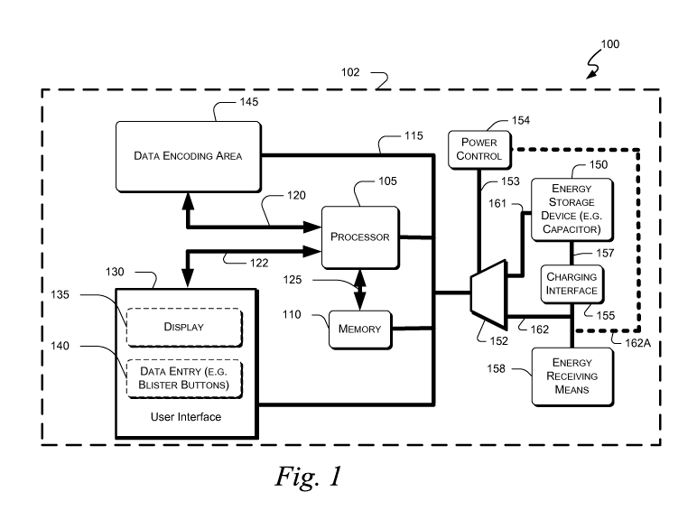
FIG. 1 depicts a block diagram of an exemplary implementation of a financial
transaction
token including a data encoding area, a charging interface, and an energy
receiving
means;
FIG. 2 illustrates possible alternate implementations of the data encoding
area seen in
FIG. 1;
FIGS. 3A-3B show front and rear views, respectively, of an exemplary
implementation of
a financial transaction token;
FIGS. 3C-3D show front and rear views, respectively, of another exemplary
implementation of a financial transaction token;
FIGS. 4A-4B show a front and rear views, respectively, of yet another
exemplary
implementation of a financial transaction token;
FIGS. 4C-4D show a front and rear views, respectively, of yet another
exemplary
implementation of a financial transaction token;
FIGS. 5A-5B show illustrations of a pendulum and piezoelectric crystal
implementation
of the charging interface seen in FIG. 1;
FIG. 6 illustrates an exemplary process for the use of various contemplated
implementations a financial transaction token;
FIG. 7 illustrates in perspective view an exemplary implementation of an
assembly
including an embedded capacitor, a cross section removed for illustration;
FIG. 8 illustrates in perspective view another exemplary implementation of an
assembly
including a multilayer embedded capacitor, a cross section removed for
illustration;
CA 02718981 2010-09-17
WO 2009/117609 PCT/US2009/037712
FIG. 9 illustrates in perspective view a portion of an exemplary
implementation of an
assembly including a multilayer embedded capacitor, a cross section removed
for
illustration, and showing electrical layer interconnect in expanded view;
FIG. 10 illustrates in perspective view a portion of another exemplary
implementation of
5 an assembly including a multilayer embedded capacitor and electrical
connection thereof,
a cross section removed for illustration;
FIG. 11 illustrates in perspective view an exemplary implementation of an
assembly with
a cavity for inserting a capacitor;
FIG. 12 illustrates in perspective view another exemplary implementation of an
assembly
with a cavity for inserting a capacitor and a backup energy source;
FIGS. 13A-13B illustrate two additional exemplary embodiments for assemblies
comprising financial transaction tokens; and
FIG. 14 illustrates another exemplary process for the use of various
contemplated
implementations a financial transaction token.
DETAILED DESCRIPTION
A block diagram for an exemplary implementation of a financial transaction
token 100 is
seen FIG. 1. The financial transaction token 100 comprises an assembly 102
that houses,
supports, and/or integrates the components shown in FIG. 1. Those of skill in
the relevant arts
understand that the assembly 102 may be integrated within a consumer product,
and nonlimiting
examples include cell phones or PDAs such as depicted in FIGS 13A and 13B, or,
in the
alternative, the assembly 102 may comprise a financial token such as those
depicted in FIGS.
3A-3D and 4A-4D. The financial transaction token includes a processor 105,
which those of
skill in the relevant arts will appreciate may comprise a microprocessor chip,
a microcontroller
chip, an ASIC, a digital signal processor (DSP), a Field Programmable Gate
Array, a wired logic
chip, or a smart card chip. The processor 105 is coupled to a power circuit
115. The power
circuit 115 provides power to the token's electronic components 105, 110, 130,
and 145, and
may further include signals indicating charging or connection status. The
processor 105 is
further coupled to signal busses 120, 122, and 125, which those of skill in
the relevant arts will
recognize may be comprised of a plurality of individual dedicated signal
circuits, commonly
shared signal busses, bidirectional signal circuits, unidirectional signal
circuits, or combinations
thereof. In one implementation, signal busses 120, 122, and 125 comprise a
single commonly
shared address/data bus with associated control signals. The processor is
coupled to a memory
110 through signal bus 125. The memory 110 may comprise volatile memory such
as CMOS or
DRAM memory, nonvolatile memory such as ROM, PROM, EEPROM, flash memory
(whether
CA 02718981 2010-09-17
WO 2009/117609 PCT/US2009/037712
6
NAND- or NOR-type), or combinations thereof, and such memory may be included
in total or in
part upon the same integrated circuit substrate as the processor 105. The
memory 110, if of
volatile type, may have its data values preserved by power provided by the
connected power
circuit 115. Data stored in memory 110 may include code or program
instructions which, when
executed by processor 105, performs at least part of command sequence
requested by a user
through the user interface 130.
An onboard energy storage device 150 such as a capacitor is coupled to a
stored energy
circuit 161 which energizes the power circuit 115 through switch 152. In one
implementation,
the switch 152 comprises a hard-wired circuit coupling the energy storage
device 150 to the
power circuit 115. Those of skill in the relevant arts will also recognize
that energy storage
devices such as batteries, inductors, capacitors, or combinations thereof may
be utilized to
implement the energy storage device 150 in FIG. 1. In one implementation,
energy storage
device 150 comprises a thin film capacitor, and may utilize a single
dielectric or a multilayer
configuration alternating conducting layers and dielectric layers. A number of
dielectrics such as
polyester; polypropylene; polycarbonate; polystyrene; polyimide;
polyfunctional acrylics;
amorphous hydrogenated carbon; polytetrafluoroethylene; polyxylylene, nitrides
of silicon and
aluminum, PTFE, PET, and combinations thereof may be utilized in such thin
film capacitor
implementations. One feature of such dielectrics that may be valuable in a
card-sized form
factor would be at least slight flexibility of the dielectric material,
allowing for minor bending
forces to distort the shape of the capacitor without causing loss of
connectivity or damage to the
capacitor when the capacitor is embedded in an assembly such as a financial
card.
A substantially planar thin film capacitor implementation is beneficial for
implementation
in the instant financial transaction token circuit, as the substantially
planar form factor may be
applied on a surface of a financial transaction card or token, or may be
wholly or partially buried
within a cavity defined within the substrate of a financial transaction card
or token 100.
Implementation of the energy storage device 150 as a single or multilayer
capacitor also provides
the benefit of avoiding the use of the leakable and potentially dangerous
electrolytes associated
with batteries, while also allowing quick rechargeability. With no toxic
electrolytes needed in
the capacitor implementation, the financial transaction token 100 may be more
safely carried in a
wallet or purse, and may also be disposed of with fewer environment toxicity
concerns. In
another implementation, energy storage device 150 may be implemented with any
number of
conventional rechargeable and non-rechargeable batteries such as alkaline
batteries, lithium ion
batteries, nickel-cadmium batteries, and nickel metal hydride batteries.
CA 02718981 2010-09-17
WO 2009/117609 PCT/US2009/037712
7
The energy storage device 150, via a coupling 157, is in electrical
communication with a
charging interface 155. Those of skill in the relevant arts will readily
recognize that the charging
interface 155 may be implemented with electrical contacts to an external
charger, or may
comprise additional electrical components to switch or regulate charging
current provided to the
energy storage device 150.
In another implementation, charging interface 155 further includes one or more
piezoelectric crystals electrically connected, via coupling 157, to the energy
storage device 150,
and a movable pendulum mass that strikes the piezoelectric crystals as the
token 100 is moved.
Turning to FIG. 5A, a piezoelectric charger implementation of the charging
interface 155 is
shown. A movable pendulum mass 500 rotates 505, preferably in a substantially
planar motion,
about a pinned end 510. The pendulum mass 500 also has an impact end 525, that
is disposed
between and may strike either of two piezoelectric crystals 520, 521. As the
crystals 520, 521
are electrically coupled 157 to the energy storage device 150, impacts of the
pendulum mass 500
cause pulses of current to be delivered to the energy storage device 150 thus
charging the storage
device 150. FIG. 5B provides an illustration of the pendulum 500 moving 506 to
strike crystal
521, and likewise, the pendulum mass 500 may move the opposite direction to
strike the other
crystal 520.
Returning to FIG. 1, an energy receiving means 158 is also provided, and is
electrically
coupled via a charging circuit 162 to the charging interface 155 and the
switch 152. The energy
receiving means 158, in one embodiment, is sensitive to electromagnetic energy
such as visible
or invisible light, RF energy, ionizing radiation, communication signals from
a POS terminal, or
an electromagnetic field. In one implementation, the energy receiving means
comprises an
antenna or an inductor for receiving power via electromagnetic radiation. The
energy receiving
means 158 may also include one or more photovoltaic cells, which produce
electricity upon
exposure to light. When the energy receiving means 158 is exposed to an
appropriate
electromagnetic energy source of sufficient magnitude, the energy storage
device 150 may be
charged by the current provided by the energy receiving means 158 that was
coupled through the
charging interface 158. As the energy receiving means 158 is also coupled to
an input of the
switch 162, the token 100 may be operated from power obtained by the energy
receiving means
158. As an example, but not by way of limitation, the feedback circuit 162A
provides a coupling
for the power control 154 to sense the voltage on the circuit 162, so that
when the energy
receiving means 158 is delivering sufficient energy to the circuit 162, the
power control 154 may
operate the switch 154 to select the externally provided power from the energy
receiving means
158 in lieu of or in addition to the power provided by the internal energy
storage device 150.
CA 02718981 2010-09-17
WO 2009/117609 PCT/US2009/037712
8
The circuit in FIG. 1, in one implementation, comprises an optional
supplemental energy
storage device is provided (not shown in FIG. 1, but shown at least at
reference numeral 151 in
FIG. 4D). The supplemental device 151 may comprise a capacitor as described
above in relation
to energy storage device 150, or may comprise any number of conventional
rechargeable and
non-rechargeable batteries such as alkaline batteries, lithium ion batteries,
nickel-cadmium
batteries, and nickel metal hydride batteries. The supplemental device 151 may
optionally be
electrically coupled to the charging interface 155, though with it may be
charged, or to which it
may deliver charging current to charge the energy storage device 150. The
supplemental device
151 may be optionally coupled to the power control switch 152, so that the
power circuit 115
may be selectively energized by the energy storage device 150, the
supplemental device 151, or a
combination, based on the signal 153 provided by power control 154. In one
implementation,
power control 154 is provided through an electrical interface to an accessory
(not shown) to the
token 100, whereby the accessory commands the switching of power based on
environmental
concerns or by the charge state of the energy storage device 150, which may,
in one
implementation, be provided by a command executed by the processor 105. The
power control
154 may also be implemented through conventional voltage sensing circuitry,
whereby the
switch 152 may energize the power circuit 115 with either the output of the
energy storage
device 150 or the supplemental energy storage device 151 when the charge state
of the energy
storage device 150 does not meet a predetermined threshold in the voltage
sending circuitry.
Once the charge state of the energy storage device 150 is sensed by the power
control 154 to
have been refreshed to a sufficient predetermined level, the switch 152 may
receive a control
signal 153 to energize the power circuit 115 with the energy storage device
150 rather than the
supplemental energy storage device 151. In one embodiment, the power control
154 may sense
when neither the energy storage device 150 or the supplemental energy storage
device 151 are
capable of delivering sufficient power for a predetermined period, and may
provide input to the
processor 105, allowing execution of commands notifying a user of a low power
state and/or
prompting the user to provide an external or alternate energy source.
Continuing with FIG. 1, a user interface 130 is also provided, and is coupled
to the power
circuit 115 and to the processor 105 via signal bus 122. In one
implementation, the user
interface may include one or more conventional displays 135 that may output
text, graphics, or a
combination. The display 135 may be implemented in such formats as a liquid
crystal display, a
thin film transistor display, touch screen, or organic LED display. The user
interface 130 also
includes an optional data entry apparatus 140. In one implementation, the data
entry apparatus
140 may include an array of buttons labeled in a manner such as a QWERTY
keyboard, a touch
CA 02718981 2010-09-17
WO 2009/117609 PCT/US2009/037712
9
pad, a touch screen, or in a more simplistic implementation, as a telephone
touch pad with
alphanumeric key assignments. The interface 130 may also receive data from an
outside source
such as a wireless POS terminal, a financial institution, or a personal
computer, and may relay
the data to the integrated processor 105 through data bus 122. In one
implementation, the
buttons in the data entry apparatus 140 may comprise blister buttons commonly
known in the art.
The user interface 130 may also include an optional on/off button that
activates the card for
selecting desired account access, performing a calculation, or authenticating
a user.
A data encoding area 145 is also provided. The data encoding area receives
data and/or
commands for displaying text or graphical information from bus 120, and
receives power from
power circuit 115. As the processor 105 may select the appropriate data based
on user input to
the user interface 130, a variety of data may be provided. In one
implementation, the
information provided to the data encoding area 145 may comprise health care
information,
personal identity information, biometric data, music, video data, or a
combination thereof, and is
considered interchangeable with the term "account data" used herein.
Turning to FIG. 2, exemplary implementations 200 of the data encoding area 145
are
shown. Data encoding area 145 is shown with an optional shielding element
145A, which allows
desired electromagnetic, optical, or radiative signals to penetrate while
protecting the data
encoding area 145 from physical abuse or damage. The token 100 may optionally
have areas
outside of the data encoding area 145 shielded from physical abuse or
otherwise acceptable
forms of electromagnetic radiation. Some of the acceptable signals that are
allowed to penetrate
the shielding 145A and may include, but are not limited to, signals
accompanying a magnetic
field, RFID signals, IrDA signals, visible light, invisible light, modulated
laser, and/or modulated
RF communication signals. By way of example and not by way of limitation,
selective shielding
element 145A may comprise a clear plastic shield, conformal coatings, an
opaque plastic shield,
or a clear thin film, depending on the implementation of data encoding area
145.
Non-limiting examples of the data encoding area are shown at reference numeral
200,
and include a magnetic stripe assembly 210, an antenna and/or transceiver 220,
a display 230,
and electrical contacts 240, and a touch screen 250. The magnetic stripe
assembly 210 may
comprise, in one implementation 210A, a reprogrammable magnetic stripe 210B
that accepts
data and/or commands from the processor 105 and formats and renders that data
into a form on a
magnetic stripe that is readable by conventional merchant magnetic stripe-
reading POS
terminals. In this manner, the processor 105 may program a particular account
for use in a
transaction as a function of user input selecting the account. Alternatively,
the processor 105
may erase the magnetic stripe of the assembly 210, rendering the card useless
in the event of its
CA 02718981 2010-09-17
WO 2009/117609 PCT/US2009/037712
loss or theft. In one implementation shown 210A, the magnetic stripe assembly
210B at least
partially slidably moves 210C into and out of the assembly 102 of the token
100 (partial view
shown), allowing the token 100 to conduct a financial transaction at a point
of sale terminal that
includes a magnetic stripe reader.
5 Continuing with FIG. 2, another implementation of the data encoding area 145
is shown
as an antenna and/or transceiver 220. The antenna 220 may include commonly
used loop
inductors such as the one shown 220A or in those shown in related ISO
standards for RF-
readable smart cards. With such an interface, account data may be translated,
modulated and
transmitted in a manner acceptable by an RF contactless merchant Point-Of-
Service (POS)
10 terminal, a 802.11 WiFi or WiMax network, or by a cellular or RF
communications network.
The data encoding area 145 may also be represented with a display 230. Account
data
may be rendered in the form of an optically-readable area, such as a one
dimensional or two
dimensional bar code 230A. In this manner, merchant POS terminals may
optically scan the
display area 230 with conventional laser scanners, and obtain account
information without the
need for expensive contactless RF POS terminals. As the display is
electronically reconfigurable
with information provided by the processor 105, the token 100 may represent
any number of
accounts for transaction payment based on the user's preference and input to
the user interface
130. Also, as a security feature, the display may be blanked or filled with a
decorative or
entertaining graphic when the user has not provided an optional security
access code, pad stroke,
or pin number to the user interface 130.
External contacts 240 are yet another alternative implementation of the data
encoding
area 145 shown in FIG. 2. With the financial transaction token 100 possessing
physical contacts
such as an array of conductive pads or shapes 240A, the financial transaction
token may be
placed in physical contact with a merchant POS terminals, and the external
contacts 240 may
establish connectivity to the merchant's financial processing system. The
processor 105 may
relay account-related information to the merchant POS terminal through the
contact interface,
thereby allowing the token 100 to be utilized with the large number of
preexisting merchant POS
terminals that accept smart cards.
Alternatively, the data encoding area 145 may comprise a touch screen 250,
wherein text
and/or graphics may be displayed, and user input may be accepted by touching
selected areas of
the screen. For example, but not by way of limitation, in an implementation
shown at reference
numeral 250A, a user is prompted to tap on one of a plurality of account
descriptors, thereby
selecting an account to complete a transaction. Those of skill in the relevant
arts also appreciate
that tapping the screen may be combined with using pointing devices such as a
joystick, direction
CA 02718981 2010-09-17
WO 2009/117609 PCT/US2009/037712
11
buttons, or selection wheels. In one embodiment, a user may provide
authentication information
by touching the display 250 in specified areas to indicate sequences of pin
numbers, selected
graphical elements, or drag strokes that match a predetermined access
criterion stored within the
storage 110. As with the other implementations 210, 220, 230, and 240 of the
data encoding area
145, a combination of techniques may be utilized within the data encoding area
145 to provide
flexibility of use and ease of merchant access to account information.
Turning to FIGS. 3A-3D and 4A-4D, various and exemplary implementations of a
financial transaction card 300 are shown. The substrate of the card 300 is
substantially rigid and
thin as are conventional credit or debit cards, and possesses substantially
similar dimensions as
existing credit, debit, stored value, or smart cards. In one implementation,
the thickness of card
300 exceeds that of conventional credit, debit, or stored value cards in order
to accommodate
circuitry, electronics, displays, and/or interface elements. The substrate of
the card 300 contains
embedded processor 105 and memory 110, and a circuit topology as described in
regards to the
block diagram for token 100 of FIG. 1.
In FIG. 3A, a front side of card 300 is shown with an array of buttons 310 and
an on/off
button 305 comprising elements of the user interface 130. The front side of
the card 300 also
includes a display 135 for outputting alphanumeric text or graphics, such as
an account number
and expiration date. An array of physical contacts 350 is shown, which may be
utilized in
conjunction with data entry 140, the data encoding area 145, and/or the
charging interface 155.
Those of skill in the relevant arts will readily appreciate that the contacts
350 shown in FIGS.
3A-3D may include more or less electrical contact elements than those shown
depending on the
particular use, and may be located together or separately on any side or
portion of the card 300 as
required by merchant POS terminals, interoperability requirements, or circuit
topology.
FIG. 3C shows a front view of an alternate implementation of card 300, with a
similar
array of buttons 310 and an on/off button 305 comprising elements of the user
interface 130. An
array of physical contacts 350 is shown, which may be utilized in conjunction
with data entry
140, the data encoding area 145, and/or the charging interface 155. A display
135 is shown
encoding a barcode that may be scanned by an optical scanner available at
merchant locations,
and may relay data from processor 105 (embedded, not shown) to provide account-
related or
other data. A display 230 as part of an implementation of the data encoding
area 145 is also
shown, with a 2-d barcode illustrated that is readable by optical means to
provide account-related
or other data that was relayed by the processor 105. Those of skill in the
relevant arts will
recognize that such combination of features may be interchanged with those
described in other
aspects of the financial transaction token.
CA 02718981 2010-09-17
WO 2009/117609 PCT/US2009/037712
12
FIG. 4A shows a front view of another implementation of card 300, with a
similar array
of buttons 310 and an on/off button 305 comprising elements of the user
interface 130. An array
of physical contacts 350 is shown, which may be utilized in conjunction with
data entry 140, the
data encoding area 145, and/or the charging interface 155. The user interface
130 of the card
shown in FIG. 4A also includes a touch pad or touch screen 405. The touch pad
or screen 405
accepts inputs from physical contact by either a stylus, pen, or fingertip,
and in one
implementation, allows a user to provide input such as entering a facsimile of
a pre-stored glyph
to authorize use of the card.
In one implementation, the user turns on the card by depressing the on/off
button 305,
then produces a stroke on the pad/screen 405 by dragging a fingertip or stylus
across the pad or
screen area 405 to reproduce a symbol or glyph substantially similar to a
symbol pre-
programmed into the processor 105 and memory 110 (embedded, not shown). Once
the symbol
or glyph is entered by the user on the pad/screen 405, the processor compares
its features with a
pre-stored graphical implementation and if the symbol's features are within a
predetermined
range, the card 300 is enabled for use, otherwise an invalid entry message is
output to display
135 and use is further inhibited until the successful glyph or symbol is
entered.
FIG. 4C shows a front view of yet another implementation of card 300, with a
similar
array of buttons 310 and an on/off button 305 comprising elements of the user
interface 130. An
array of physical contacts 350 is shown, which may be utilized in conjunction
with data entry
140, the data encoding area 145, and/or the charging interface 155. The user
interface 130 of the
card shown in FIG. 4C also includes a touch pad or touch screen 405. The touch
pad or screen
405 accepts inputs from physical contact by either a stylus, pen, or
fingertip, and in one
implementation, allows a user to provide input such selecting an account to be
used to provide
payment for a transaction, and an indicia of an account, such as a bar code,
may subsequently be
output on a display 135 to consummate a transaction.
FIGS. 3B, 3D, 4B, and 4D show rear views of respective implementations of a
financial
transaction card 300. The card 300 has a magnetic stripe 330 which like
conventional magnetic
stripe fields, is readable in preexisting merchant POS terminals or ATMs. The
magnetic stripe
330, as part of the data encoding area 145 and magnetic stripe assembly 210
may optionally be
programmable by data and commands sent from the embedded processor 105 and
memory 110.
Also shown on the card 300 is an optional array of physical contacts 350,
which, as
described above may be utilized in conjunction with data entry apparatus 140,
the data encoding
area 145, and/or the charging interface 155. Those of skill in the relevant
arts will also recognize
that other of the aforementioned data encoding elements 145 or user interface
elements 130 may
CA 02718981 2010-09-17
WO 2009/117609 PCT/US2009/037712
13
reside on the back surface of the card 300, and this orientation may be
preferential to preserve
account security or allow additional features on a limited card area.
An energy storage device 150 is shown embedded in the card 300 in FIGS. 3B,
3D, and
4D, and may comprise a thin film capacitor. Those of skill in the relevant
arts will recognize that
such a capacitor may be applied to the surface of the card 300 as shown in
FIG. 4B at reference
numeral 150 rather than being located within a substrate cavity in the card
300, and may have an
optional protective film, conformal coating, or encapsulant added to protect
the capacitor.
Additional implementations of the energy storage device 150 will be discussed
in more detail
below in regards to FIGS. 7-12. Those of skill in the relevant arts will also
recognize that an
energy storage device 150 may comprise any number of shapes, not necessarily
rectilinear, and
may occupy significantly all or part of the cross sectional area defined by
the outer perimeter of
the card 300. In the illustration shown in FIG. 3B, for example, the energy
storage device 150
spans covers an area approximately two thirds of the cross-sectional area of
the card 300 but
could be configured to cover more or less area depending on the amount of
energy storage
desired and the particular layout of the card's circuitry. In FIG 3D, the
buried energy storage
device 150 resides under the magnetic stripe 330 and does not occupy space in
proximity to the
physical contacts 350. In another embodiment FIG 4D, of card 300, a
supplemental energy
storage device 151 is also included, and optionally may be embedded in the
card 300.
FIG. 6 illustrates an exemplary process 600 for the use of various
implementations of a
financial transaction token such as financial transaction token 100 seen in
FIG. 1. In step 610 the
financial transaction token 100 or card 300 is turned on so that the processor
105 may assume an
active state and operate by retrieving and executing program instructions
stored in the memory
110. The power-on condition may be triggered by one or more of the following
conditions: (a)
inserting the token 100 or card 300 into a merchant POS terminal and making
contact between
electrical contacts in the token 100 or card 300 and the merchant POS
terminal; (b) inserting the
token 100 or card 300 into a user device such as a cell phone, PDA, charger,
or accessory; (c)
attaching an electrical connector such as a USB or Firewire connector to the
token 100 or card
300; (d) depressing an on/off button 305 and/or holding the on/off button down
for a
predetermined period of time; (e) depressing a general purpose button 310; (f)
touching a touch
screen or touch pad 405; or (g) bringing a token 100 or card 300 equipped with
an
antenna/transceiver 220 within range of an RF merchant POS terminal. Once the
token 100 or
card 300 has been turned on, a display 135 or 230 may optionally display an
indicia that the card
is on and ready for use and/or authentication.
CA 02718981 2010-09-17
WO 2009/117609 PCT/US2009/037712
14
In step 620, the user is optionally authenticated, so that lost or stolen
cards may not be
used by an unauthorized party. Tokens 100 or cards 300 utilizing this step
will not be usable to
furnish data or complete financial transactions until the authentication
requirement has been
satisfied. The requirement can be met a number of ways: (a) the user or
cardholder drags a
fingertip or stylus across the pad or screen area 405 to reproduce a symbol or
glyph substantially
similar to a symbol pre-programmed into the processor 105 and memory 110, and
once the
symbol or glyph is entered by the user on the pad/screen 405, the processor
compares its
features with a pre-stored representation of a graphical element to determine
that the entered
symbol's features are within a predetermined range when compared to the pre-
stored
representation; (b) the user or cardholder enters a pin number or passphrase
into the card's user
interface 130 such as by depressing a series of keys 310 or touching labeled
locations on a touch
pad or touch screen 405, and the pin or passphrase matches a respective
reference pin or
passphrase pre-stored in the memory 110; (c) a biometric aspect of the user or
cardholder is
scanned and compared to a predetermined biometric value pre-stored in the
memory 110; or (d)
the card is used in a preauthorized context such as certain trusted merchants,
the identity of
which is stored in the memory 110. If authorization fails, the user or
cardholder is notified by an
optional output on a display 135, and authorization may be re-attempted.
Optionally, if a
predetermined number of unsuccessfully attempts occurs, the token 100 or card
300 is locked out
from further transactions until a reset of the token 100 or card 300 occurs by
an authorized party.
If the optional authorization succeeds, the card is enabled for use.
In optional step 630, the user or cardholder provides input to the token 100
or card 300 to
conduct an operation such as selecting an account for which to provide payment
for a
transaction, performing a calculation, obtaining stored data, storing new
data, or modifying user
data parameters such as a pin number, passphrase, or authorization glyph or
symbol. If no user
input is provided, the token 100 or card 300 will be configured to a default
state, which may
include the previous state or condition of the card when last used. If an
account for a transaction
or a request for information is selected, the processor 105 obtains the
respective data from the
memory 110 and renders the to the data encoding area 145 in a form appropriate
for the
particular mode of output 200. Thus, a token 100 or card 300 may be configured
for a particular
use, for instance for a user's personal credit account versus that user's
business account, or for a
particular issuer's account among many that are available to the user. For
example, if a
cardholder's personal Visa account was selected, the reprogrammable magnetic
stripe 330 could
be reprogrammed to provide information related to that personal Visa account
from the values
stored in memory 110.
CA 02718981 2010-09-17
WO 2009/117609 PCT/US2009/037712
Once the token 100 or card 300 is ready for use, data is transferred to the
intended
destination. This may occur by (a) the user or cardholder reading an output
from a display 135;
(b) a merchant obtaining data through a scan of the magnetic stripe 330; (c) a
merchant optically
scanning a barcode that is displayed in a data encoding area 145; (d) a
merchant reading an
5 electromagnetic signal transmitted from the data encoding area 145; (e) the
merchant receiving
data through electrical contacts of the merchant's POS terminal that are in
physical contact with
those provided on the token 100 or card 300; or (f) data is obtained through
an electrical
connector attached to the token 100 or card 300. Once the data is transferred,
for instance, a
merchant may complete a financial transaction using the data provided by the
token 100 or card
10 300.
Optionally, after the data is transferred 640, the token 100 or card 300 is
secured 650 so
that only authorized parties may access the token 100 or card 300 and then
turned off 660 so that
the processor 105 may assume a standby state to conserve energy on the onboard
energy storage
device 150. This optional securing step 650 and the poweroff step 660 may be
initiated through
15 one or more of the following techniques: (a) allowing a predetermined
period of time to pass
without inputting any information to the user interface 130; (b) removing the
token 100 or card
300 from contact a merchant POS terminal; (c) breaking contact between
electrical contacts in
the token 100 or card 300 and a merchant POS terminal, charging device,
external power source,
or conventional electrical connector (e.g.; USB (Universal Serial Bus) or
FirewireTM (IEEE
1394)) or single wire protocol in the case of a smart card chip; (d) removing
the token 100 or
card 300 from a user device such as a cell phone, PDA, charger, or accessory;
(e) depressing an
on/off button 305 and/or holding the on/off button down for a predetermined
period of time; (f)
depressing a predetermined sequence of general purpose buttons 310; (f)
touching a
predetermined area of touch screen or touch pad 405; or (g) removing the token
100 or card 300
equipped with an antenna/transceiver 220 from the range of an RF merchant POS
terminal.
Once the appropriate condition has occurred to initiate shutdown, optionally,
the token 100 or
card 300 erases its reprogrammable magnetic stripe 330, refuses additional
inputs except power
on and/or authentication inputs, and/or encrypts data stored in the memory
110. Optionally, an
indicia may be output to a display 135, indicating that the card is locked and
secured.
Turning to Fig. 7, a perspective view an exemplary implementation of an
assembly 102
including an embedded single-layer capacitor is shown. The dimensions 730,
740, and 750 of
the substantially planar substrate 760 may approximate the dimensions of a
conventional credit
card, with possible deviations to incorporate additional features or elements.
A portion 700 of
the substrate 760 has been removed from the drawing to illustrate a cross
section of a portion of
CA 02718981 2010-09-17
WO 2009/117609 PCT/US2009/037712
16
the assembly 102. Within the substrate 760 of the assembly 102 is embedded a
capacitor 150.
In the illustrated implementation, the capacitor comprises a pair of
substantially planar and
parallel conductive electrodes 710, 720, separated by a substantially planar
dielectric layer 730.
The dielectric utilized may be selected based upon with the requirements of
the application, and
for example, but not by way of limitation, may comprise polyester;
polypropylene;
polycarbonate; polystyrene; polyimide; polyfunctional acrylics; amorphous
hydrogenated
carbon; polytetrafluoroethylene; polyxylylene, nitrides of silicon and
aluminum, PTFE, PET,
and combinations thereof. Although a single capacitor 150 is shown, those of
skill in the
relevant arts appreciate that two or more capacitors may be embedded within
the assembly 102.
Those of skill in the relevant arts also appreciate that the dielectric 730
may be comprised of the
same or a different material than the substrate 760 of the assembly 102. Those
of skill in the
relevant arts understand that the capacitor 150 may comprise a thin film
capacitor. The capacitor
150 is interconnected to the token 100 as described in relation to FIG. 1
above.
Turning to FIG. 8 a perspective view an exemplary implementation of an
assembly 102
including an embedded multi-layer capacitor is shown. Similarly to FIG. 7, the
assembly 102
comprises a substantially planar substrate 760 which may approximate the
dimensions of a
conventional credit card, with possible deviations to incorporate additional
features or elements.
A portion 700 of the substrate 760 has been removed from the drawing to
illustrate a cross
section of a portion of the assembly 102. Within the substrate 760 is included
a multilayer
capacitor 150, which is comprised of an even number of conductive electrodes,
and in the
illustrated implementation, six electrodes are used (800, 801, 802, 803, 804,
and 805), although
those of skill in the relevant arts understand that more or fewer electrodes
could be used.
Similarly to FIG. 7, the electrodes are conductive, and are substantially
planar and parallel, and
are separated by a dielectric as described in more detail in regards to FIG.
9.
Turning to FIG. 9, a closer prospective view is provided of a portion of the
substrate 760
of the assembly 102 shown in FIG. 8. A cross-sectional view of the layer stack
900 is enlarged
to show detail, and illustrates a cross section of substantially planar and
parallel conductive
electrodes (800, 801, 802, 803, 804, and 805) separated by a dielectric 920.
Those of skill in the
relevant arts appreciate that the dielectric 920 may comprise the same or
different substance than
the material that comprises the bulk of the substrate 760. The material
comprising the bulk of
the substrate 760, whether or not comprised of the same material as the
dielectric 920, may cover
the top 910 and cover the bottom 930 of the capacitor stack 900. The layer
stack 900 may
comprise a thin film multilayer capacitor, and/or may be constructed by
alternative application of
conductive layers and dielectric layers, assembly of successive
conductive/dielectric layers,
CA 02718981 2010-09-17
WO 2009/117609 PCT/US2009/037712
17
inclusion of a pre-assembled capacitor assembly, or by a combination of
stacking conductive
layers, dielectric layers, and conductive layers that are in whole or part
oxidized. Those of skill
in the relevant arts also appreciate that a multilayer capacitor can be formed
from any even
number of four or more alternatively interconnected conductive electrodes with
intervening
dielectrics, and in some embodiments may comprise thousands of layers, thereby
providing for
capacitances in the value ranges of picroFarads to several Farads.
Continuing with FIG. 9, an interconnection of the capacitor 150 is also
provided. The
conductive electrodes (800, 801, 802, 803, 804, and 805) are disposed to
create non-fully
overlapping zones 901, 902, in which only alternate conductive electrodes
overlap. For example,
in zone 901, only the odd-numbered conductive electrode planes 801, 803, and
805 overlap, and
in zone 902, only the even-numbered planes 800, 802, and 804 overlap.
Therefore, conductive
vertical columns, or vias, 940, may provide for interconnection in the partial
overlap zones 901,
902. As the vias 940 contact the conductive layers through which they
penetrate, a multilayer
capacitor can be formed by connecting the vias within the zone 901 to one
polarity of the
capacitor circuit, and the vias within zone 902 to the opposite polarity in
the capacitor circuit.
Those of skill in the relevant arts appreciate that the vias 940 may comprise,
but not by way of
limitation, any shape of conductive substance such as copper, aluminum, tin,
solder, or
conductive paste, and may be formed by any number of techniques including a
drill-and-plate
process or by an etch and fill process. The capacitor 150 is coupled to the
circuitry of the token
100 as described in relation to FIG. 1 above.
Turning to FIG. 10, an alternative embodiment of the interconnection approach
shown in
FIG. 9 is illustrated. Again, a portion of the substrate 760 of the assembly
102 shown with layers
of the capacitor 150 appearing, but the interconnection in zones 901, 902, are
in communication
with approximately rectilinearly-shaped conductive channels 1000 that
electrically connect
alternating conductive layers as described in relation to FIG. 9. Similarly to
FIG. 9, dielectric is
disposed between each of the substantially parallel planar electrodes, forming
a capacitor 150.
Those of skill in the relevant arts appreciate that the conductive channels
1000 may comprise,
but not by way of limitation, any shape of conductive substance such as
copper, aluminum, tin,
solder, or conductive paste, and may be formed by any number of techniques
including a drill-
and-plate process or by an etch and fill process.
Turning to FIG. 11, a perspective view of an implementation of the assembly
102 is
shown. Similarly to FIG. 7, the assembly 102 comprises a substantially planar
substrate 760
which may approximate the dimensions of a conventional credit card, with
possible deviations to
incorporate additional features or elements. The assembly 102 further
comprises a recess or void
CA 02718981 2010-09-17
WO 2009/117609 PCT/US2009/037712
18
1100, which is sized to receive an energy storage device 150 such as a
capacitor. Once the
device 150 is installed in the recess 1100, a flush or substantially flush fit
allows the application
of a substantially planar top layer (not shown) to the top surface of the
substrate 760 to cover the
installed device 150. In one embodiment, the device 150 comprises a thin film
capacitor,
interconnected to the circuitry of FIG. 1 as described in relation thereto.
Turning to FIG. 12, an alternative perspective view of an implementation of
the assembly
102 is shown. Similarly to FIG. 7, the assembly 102 comprises a substantially
planar substrate
760 which may approximate the dimensions of a conventional credit card, with
possible
deviations to incorporate additional features or elements. The assembly 102
further comprises a
recess or void 1100, which is sized to receive energy storage device 150, and
supplemental
energy storage device 151. Once the devices 150, 151 are installed in the
recess 1100, a flush or
substantially flush fit allows the application of a substantially planar top
layer (not shown) to the
top surface of the substrate 760 to cover the installed device 150. In one
embodiment, the energy
storage device 150 comprises a thin film capacitor and supplemental energy
storage device 151
comprises a backup battery, both of which are interconnected to the circuitry
of FIG. 1 as
described in relation thereto.
Turning to FIG. 13A, an alternate implementation of the token 100 is shown as
a
communications device such as a cell phone. The assembly 102 includes a slot
323 for a
financial card 300 (nonlimiting embodiments of which are shown in FIGS. 3A-3D,
4A-4D), or
optionally, the financial card 300 is permanently or semi-permanently
integrated within the
hardware of the token 100. The token 100 has a display 230, and a data entry
keypad 140,
allowing interaction with the assembly 102 to accept user commands. As
mentioned previously,
the token 100 may be used to complete a financial transaction without removing
card 300, or the
token 100 may configure the card 300, using commands entered through the user
interface 130,
to select a particular transaction payment account to be transmitted to the
token through the
internal electrical interface (not shown). In a similar spirit, FIG. 7B
illustrates another
implementation of the token 100, shown as a consumer device such as a personal
digital assistant
(PDA). The assembly 102 includes a slot 323 for a financial token 300, or
optionally, the
financial token 300 is permanently or semi-permanently integrated within the
hardware of the
token 100. The token 100 has a touch screen display 250A for entry and output
of commands
and data, a data buttons and pads 140. As mentioned above, the token 100 may
also be used to
complete a financial transaction without removing card 300, or the token 100
may configure the
card 300, using commands entered through the user interface 130, to select a
particular
CA 02718981 2010-09-17
WO 2009/117609 PCT/US2009/037712
19
transaction payment account to be transmitted to the token through the
internal electrical
interface (not shown).
FIG. 14 illustrates an exemplary process 1400 for the use of various
implementations of a
financial transaction token such as financial transaction token 100 seen in
FIG. 1 or the financial
card 300. In step 1410 the financial transaction token 100 or card 300 is
exposed to an
electromagnetic energy source such as visible or invisible light, RF energy,
ionizing radiation,
communication signals from a POS terminal, or an electromagnetic field.
Alternatively, the
energy receiving means 158 of the financial token 100 or card 300 is
separately exposed to such
an electromagnetic energy source, which may be the case if the token 100
possesses an external
antenna comprising the energy receiving means 158. In step 1420 the
electromagnetic energy
from the external source is captured by the energy receiving means 158 and
delivered to the
circuitry of the token 100 or card 300. In one implementation, but not by way
of limitation, such
energy capturing and conversion may occur by coupling an electromagnetic
magnetic field
through an inductor, electromagnetic radiation through an antenna, or light
through a
photovoltaic cell.
In step 1430, the token 100 or card 300 senses a change in voltage and/or
current in the
output of the energy receiving means 158, and if this change indicates that a
sufficient external
electromagnetic energy source is available to power the token 100 or card 300
through the
energy receiving means 158, a switch may be optionally operated to enable the
energy receiving
means 158 to provide operating power to the electronic components 145, 105,
130, 150, 154,
155, 151, of the token 100 or card 300. Such operating power may be
supplemented by the
energy storage device 150, or supplemental energy storage device 151, by
operating the switch
152 to select the desired energy source or combination of sources.
Upon sensing 1430 the change in conditions, the token 100 or card 300 becomes
active
1440, allowing its electronic circuitry 145, 105, 130, 150, 154, 155, 151, to
be operated so as to
initiate or complete a financial transaction. For example, in optional step
1450, a user is queried
through the user interface 130 to select an account for use in a transaction.
If no selection was
offered, a default account may be selected in lieu of user input.
Once the account choice is entered or default account data selected, the token
100 or card
300 is configured with the appropriate account-related information to enable
the token 100 or
card 300 to be used to provide payment for a financial transaction. As non-
limiting examples,
account information may be provided to and rendered in the data encoding area
145, such as by
displaying a bar code representing the account information, transmitting an RF
communication
signal indicating account information to a POS terminal, transmitting a
modulated light beam
CA 02718981 2010-09-17
WO 2009/117609 PCT/US2009/037712
indicating account information to a POS terminal, displaying an account
number, or providing
electrical signals for electrical contacts in communication with a POS
terminal.
In step 1470, a voltage and/or current change is sensed by the token 100 or
card 300 in
the charging circuit 162. This change, in one embodiment, indicates an
undesirable fluctuation
5 or decline of the charging circuit 162 voltage, or may otherwise comprises
sensed conditions that
indicate that the external electromagnetic energy source that is providing
power to the energy
receiving means 158 is no longer sufficient to provide operating power to the
electronic
components 145, 105, 130, 150, 154, 155, 151, of the card 100 or token 300.
Such may be the
case if the token 100 or card 300 is being removed from proximity to a POS
terminal, or when
10 light provided to a photovoltaic cell of the token 100 or card 300 is being
interrupted, or if the
token 100 or card 300 is being removed from a wireless charger. In these
cases, the switch 152
may be operated to energize 1480 the power circuit 115 with energy provided
by, in whole or
part, the energy storage device 150 and/or supplemental device 151. In this
manner, the token
100 or card 300 may continue to operate when externally provided energy is
insufficient or
15 otherwise inhibited.
Step 1490 optionally indicates a step that when the token 100 or card 300 is
switched to
an internal energy source under a loss of sufficient external electromagnetic
energy. In this case
the user is prompted through the user interface 130 whether the token 100 or
card 300 is to be
shut down or otherwise placed into an inactive state. If the user so specifies
by entering an
20 indicia through the user interface 130, the processor 105 takes action to
bring the processor into
an inactive state or energy conserving mode. Optional step 1495 also depicts a
condition where
the processor 105 of the token 100 or card 300 begins a countdown sequence
upon the switching
1480 to the internal source 150 and/or 151. The purpose of this countdown is
to turn off the
token 100 or card 300 after a predetermined time interval if the internal
energy source is enabled
and the token 100 or card 300 is not in use, thereby preventing inadvertent
discharge of the
power source 150 and/or 151. The user may, through the user interface 130,
abort the timeout
automatic shutdown by entering any indicia that the token 100 or card 300 is
to remain in active
condition.
The steps of a method, process, or algorithm described in connection with the
implementations disclosed herein may be embodied directly in hardware, in a
software module
executed by a processor, or in a combination of the two. The various steps or
acts in a method or
process may be performed in the order shown in FIGS. 6, or 14 or may be
performed in another
order. Additionally, one or more process steps may be omitted or one or more
process steps may
CA 02718981 2010-09-17
WO 2009/117609 PCT/US2009/037712
21
be added to the processes. An additional step, block, or action may be added
in the beginning,
end, or intervening existing elements of such processes.
The above description of the disclosed embodiments is provided to enable any
person of
ordinary skill in the art to make or use the disclosure. Various modifications
to these
embodiments will be readily apparent to those of ordinary skill in the art,
and the generic
principles defined herein may be applied to other embodiments without
departing from the spirit
or scope of the disclosure. Thus, the disclosure is not intended to be limited
to the embodiments
shown herein but is to be accorded the widest scope consistent with the
principles and novel
features disclosed herein.