Note: Descriptions are shown in the official language in which they were submitted.
CA 02719014 2010-09-20
WO 2009/120851 PCT/US2009/038375
METHOD AND APPARATUS FOR RESETTING SILICON CONTROLLED
RECTIFIERS IN A HYBRID BRIDGE
CROSS-REFERENCE TO RELATED APPLICATIONS
[0001] This application claims benefit of United States provisional patent
application serial number 61/070,798, filed March 26, 2008, which is herein
incorporated in its entirety by reference.
BACKGROUND OF THE INVENTION
Field of the Invention
[0002] Embodiments of the present disclosure generally relate to power
conversion and, more particularly, to a method and apparatus for controlling
Silicon
Controlled Rectifiers (SCR) in a hybrid H-bridge.
Description of the Related Art
[0003] A common topology for DC-AC inverters employs a DC-DC booster stage
followed by an H-bridge. The H-bridge acts to create a true AC waveform at the
inverter output by "unfurling" a rectified sine wave received from the DC-DC
booster
stage. In some instances, the AC output of the DC-AC inverter may be coupled
to a
commercial power grid, and the H-bridge operates at the frequency of the AC
line
voltage on the grid. For example, distributed generators (DGs), such as solar
power
systems, convert DC power generated by renewable resources to AC power that
may be coupled to the grid.
[0004] Many DC-AC inverters employ Silicon Controlled Rectifiers (SCRs) as the
H-bridge switching elements due to their robustness, easy drive, and low cost.
However, in systems where the DC-AC inverter output is coupled to the grid,
anomalies occurring in the AC line voltage may induce a commutation failure in
such
an H-bridge. For example, if the AC line voltage suddenly reverses polarity
prior to
its normal zero crossing, the active SCRs in the H-bridge may erroneously
remain in
a conductive state ("on") during the next half of the AC line voltage cycle
while the
previously inactive SCRs are also switched on. This effectively "shorts" the
CA 02719014 2010-09-20
WO 2009/120851 PCT/US2009/038375
H-bridge, resulting in an uncontrolled current surge through the inverter and
subsequent damage to the inverter.
[0005] Therefore, there is a need for a method and apparatus for controlling
Silicon Controlled Rectifiers (SCR) in an H-bridge.
SUMMARY OF THE INVENTION
[0006] Embodiments of the present invention generally relate to a method and
apparatus for resetting Silicon Controlled Rectifiers (SCRs) in an H-bridge.
The
apparatus comprises a hybrid bridge, comprising at least one SCR and at least
one
switch, and an abnormal current detector, coupled to the hybrid bridge. The
abnormal current detector detects an abnormal current in the hybrid bridge and
drives the at least one switch to control current flow through the hybrid
bridge.
BRIEF DESCRIPTION OF THE DRAWINGS
[0007] So that the manner in which the above recited features of the present
invention can be understood in detail, a more particular description of the
invention,
briefly summarized above, may be had by reference to embodiments, some of
which
are illustrated in the appended drawings. It is to be noted, however, that the
appended drawings illustrate only typical embodiments of this invention and
are
therefore not to be considered limiting of its scope, for the invention may
admit to
other equally effective embodiments.
[0008] Figure 1 is a block diagram of a power conversion module in accordance
with one or more embodiments of the present invention;
[0009] Figure 2 is a schematic diagram of an abnormal current detector in
accordance with one or more embodiments of the present invention;
[0010] Figure 3 is a schematic diagram of an abnormal current detector in
accordance with one or more embodiments of the present invention; and
2
CA 02719014 2010-09-20
WO 2009/120851 PCT/US2009/038375
[0011] Figure 4 is a flow diagram of a method for resetting SCRs in a hybrid
bridge in accordance with one or more embodiments of the present invention.
DETAILED DESCRIPTION
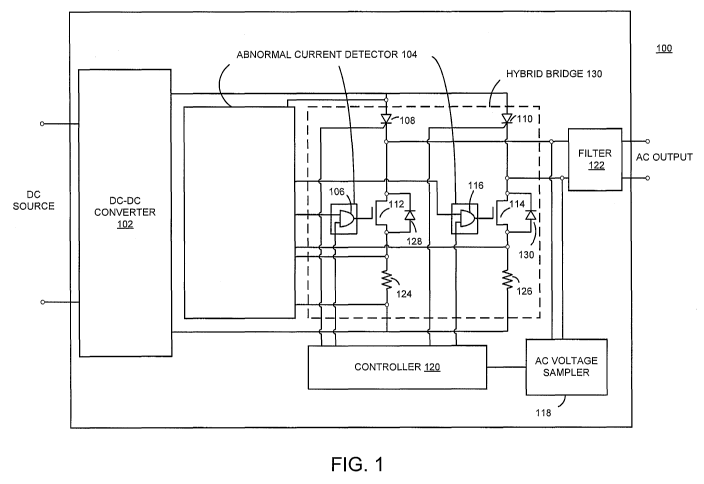
[0012] Figure 1 is a block diagram of a power conversion module 100 in
accordance with one or more embodiments of the present invention. The power
conversion module 100 accepts a DC input power from a DC source and converts
such DC power to an AC output power. In some embodiments, the power
conversion module 100 may be employed in a DG, such as a solar power system,
for converting DC power from one or more photovoltaic (PV) modules to AC power
that is coupled to an AC commercial power grid.
[0013] The power conversion module 100 comprises a DC-DC converter 102, an
abnormal current detector 104, a hybrid H-bridge ("hybrid bridge") 130, a
controller
120, an AC voltage sampler 118, and a filter 122. In some alternative
embodiments,
the DC-DC converter 102 may be excluded from the power conversion module 100.
In other alternative embodiments, the DC-DC converter 102 may be external to
the
power conversion module 100 and coupled to the power conversion module 100. In
such embodiments, a single DC-DC converter 102 may be coupled to a single
power conversion module 100; alternatively, multiple DC-DC converters 102 may
be
coupled to a single power conversion module 100.
[0014] The DC-DC converter 102 is coupled to the hybrid bridge 130 and the
controller 120. The DC-DC converter 102 accepts a DC input voltage and
converts
the DC input voltage to a DC output voltage in accordance with DC-DC
conversion
control signals received from the controller 120. The DC output voltage from
the
DC-DC converter 102 is then coupled to the hybrid bridge 130 through the
abnormal
current detector 104. The hybrid bridge 130 is coupled to the controller 120
and
converts the received DC voltage to an AC output voltage in accordance with DC-
AC conversion control and switching signals received from the controller 120.
Such
AC output voltage is then coupled to the AC commercial power grid ("grid") via
the
filter 122, which acts to smooth the AC output voltage.
3
CA 02719014 2010-09-20
WO 2009/120851 PCT/US2009/038375
[0015] The hybrid bridge 130 comprises Silicon Controlled Rectifiers (SCRs)
108
and 110, switches 112 and 114, and resistors 124 and 126. In some embodiments,
diodes 128 and 130 are coupled across the switches 112 and 114, respectively,
with
anode terminals of the diodes 128 and 130 coupled to source terminals of the
corresponding switches 112 and 114. Alternatively, the diodes 128 and 130 may
be
an integral component of the switches 112 and 114. The switches 112 and 114
may
be n-channel depletion-mode metal-oxide-semiconductor field-effect transistors
(MOSFETs); alternatively, switches such as junction gate field-effect
transistors
(JFETs), insulated-gate bipolar transistor (IGBTs), and the like, may be used.
[0016] The SCR 108, switch 112, and resistor 124 are coupled in series such
that
a cathode terminal of the SCR 108 is coupled to a drain terminal of the switch
112,
and a source terminal of the switch 112 is coupled to a first terminal of the
resistor
124. Similarly, the SCR 110, switch 114, and resistor 126 are coupled in
series
such that cathode terminal of the SCR 110 is coupled to a drain terminal of
the
switch 114, and a source terminal of the switch 114 is coupled to a first
terminal of
the resistor 126. Additionally, the anode terminals of the SCRs 108 and 110
are
coupled to a first output terminal of the DC-DC converter 102 and second
terminals
of the resistors 124 and 126 are coupled to a second output terminal of the DC-
DC
converter 102. Cathode terminals of the SCRs 108 and 110 are coupled to the
filter
122 and to the AC voltage sampler 118.
[0017] The abnormal current detector 104 comprises AND gates 106 and 116
and provides a first input to each AND gate 106 and 116; the controller 120 is
coupled to a second input of each AND gate 106 and 116. Output terminals of
the
AND gates 106 and 116 are coupled to gate terminals of the switches 112 and
114,
respectively, for controlling (i.e., activating and deactivating) such
switches.
Additionally, the controller 120 is coupled to a control gate of each SCR 108
and 110
for activating (i.e., switching on) the SCRs 108 and 110, and the abnormal
current
detector 104 is coupled to the source terminals of the switches 112 and 114,
the
anode terminal of the SCR 108, and the second terminal of the resistor 124.
4
CA 02719014 2010-09-20
WO 2009/120851 PCT/US2009/038375
[0018] The controller 120 is coupled to the AC voltage sampler 118 for
obtaining
AC line voltage samples from the grid; additionally, the controller 120
obtains DC
current and voltage samples from the DC-DC controller 102. The controller 120
utilizes such samples to produce the control and switching signals for driving
the
DC-DC converter 102 and the hybrid bridge 130 to generate an AC power output
that is optimally achieved from the DC power input to the power conversion
module
100; i.e., the AC power output from the power conversion module 100 is
synchronously coupled to the grid.
[0019] In one embodiment of the present invention, the DC voltage at the
output
of the DC-DC converter 102 has the form of a full-wave rectified sine wave,
where
the frequency of the rectified sine wave is twice the frequency of the AC line
voltage
on the grid. Under normal operating conditions (i.e., no commutation failures
or
anomalies in the AC line voltage), the abnormal current detector 104 generates
an
active-high signal as the first inputs to the AND gates 106 and 116. Such an
active-
high input allows the second AND gate input signals from the controller 120 to
determine the output of the AND gates 106 and 116 and thereby control the
operation (i.e., activation and de-activation) of the switches 112 and 114.
The
controller 120 sequentially activates the hybrid bridge diagonals (i.e., SCR
108/switch 114 and SCR 110/ switch 112) at AC line voltage zero-crossings in a
mutually exclusive fashion such that each diagonal conducts current for half
of the
AC line voltage cycle. For example, the diagonal SCR 108/switch 114 conducts
during a first half of the AC line voltage cycle while the diagonal
SCR110/switch 112
remains off and does not conduct.
[0020] When the diagonal SCR 108/switch 114 is conducting, the current through
the diagonal drops to zero at the next AC line voltage zero-crossing as the DC
voltage across the hybrid bridge 130 drops to zero, causing the SCR 108 to
deactivate. Additionally, the controller 120 generates an active-low input at
the
second input to the AND gate 116, causing the subtending switch 114 to
deactivate,
and activates the previously inactive diagonal SCR110/switch 112. During the
subsequent half of the AC line voltage cycle, the SCR 108 remains reverse-
biased
CA 02719014 2010-09-20
WO 2009/120851 PCT/US2009/038375
(i.e., off) and the controller 120 continues to generate an active-low input
to the AND
gate 116 to keep the switch 114 off.
[0021] At the next AC line zero-crossing, the diagonal SCR110/switch 112
becomes inactive, while the diagonal SCR 108/switch 114 again becomes active.
Such operation "unfurls" the full-wave rectified sine wave input to the hybrid
bridge
130 to generate a true AC waveform at the output of the hybrid bridge 130 that
is in
phase with the line voltage on the grid.
[0022] In accordance with one or more embodiments of the present invention,
the
abnormal current detector 104 acts to detect an abnormal current in the hybrid
bridge 130, such as a negative current or an excessive positive current, and
accordingly drives the switches 112 and 114 to control the flow of current
through
the hybrid bridge 130. Such an abnormal current may be caused by a commutation
failure or an abnormality in the AC waveform on the grid and may be capable of
causing one of the SCRs to operate improperly. Upon detecting the abnormal
current, the abnormal current detector 104 generates an active-low input to
the AND
gates 106 and 116, thereby driving the switches 112 and 114 to deactivate
(i.e.,
switch off) and interrupting current flow through the hybrid bridge 130. Such
current
interruption immediately resets the SCRs 108 and 110 and averts any damage to
the power conversion module 100. The abnormal current detector 104 further
sustains the active-low input to the logic gates 106 and 116, and thus the
current
interruption, for a time period (i.e., a stabilization period) sufficient to
allow the
anomaly causing the abnormal current to clear before operation of the hybrid
bridge
130 resumes.
[0023] After the stabilization period, the abnormal current detector 104 again
generates an active-high input to the AND gates 106 and 116, allowing the
controller
120 to once again determine the operating state of the switches 112 and 114.
Normal operation of the power conversion module 100 resumes at the next zero-
crossing of the AC line voltage, at which point the controller 120 will
activate the
appropriate diagonal pair (i.e., SCR 108/switch 114 or SCR 110/switch 112).
6
CA 02719014 2010-09-20
WO 2009/120851 PCT/US2009/038375
[0024] Figure 2 is a schematic diagram of an abnormal current detector 104 in
accordance with one or more embodiments of the present invention.
[0025] The abnormal current detector 104 comprises resistors 202, 208, and
212,
capacitor 204, transistors 206 and 210, and a Schmitt trigger 214. In some
embodiments, the transistors 206 and 210 are npn Bipolar Junction Transistors
(BJTs); alternatively, other types of transistors or comparators may be
utilized.
Collector terminals of the transistors 206 and 210 are coupled to an input of
the
Schmitt trigger 214, a first terminal of the resistor 202, and a first
terminal of the
capacitor 204. A second terminal of the resistor 202 is coupled to the anode
terminal of the SCR 108, and a second terminal of the capacitor 204 is coupled
to
base terminals of the transistors 206 and 210, and the second terminals of the
resistors 124 and 126. Emitter terminals of the transistors 206 and 210 are
coupled
to first terminals of the resistors 208 and 212, respectively, and second
terminals of
the resistors 208 and 212 are coupled to the first terminals of the resistors
124 and
126, respectively. Additionally, an output from the Schmitt trigger 214 is
coupled to
the first input of each AND gate 106 and 116. During normal operation, the
transistors 206 and 210 are in an off state and the capacitor 204 maintains an
active-high input to the Schmitt trigger 214, resulting in an active-high
output from
the Schmitt trigger 214 to the AND gates 106 and 116.
[0026] During operation of the hybrid bridge 130, for example during a portion
of
the AC line voltage cycle when the diagonal SCR 110/switch 112 is conducting
("on") and the diagonal SCR 108/switch 114 is not conducting ("off'), a
commutation
failure or anomaly on the AC line voltage may cause a negative current through
the
resistor 126 and the switch 114. The negative current results in a sufficient
base
voltage at the transistor 210 to cause the transistor 210 to activate (i.e.,
switch on),
thereby discharging the capacitor 204. The resulting voltage drop at the input
to the
Schmitt trigger 214 generates an active-low input to the AND gates 106 and
116,
thereby switching off the switches 112 and 114, interrupting current flow
through the
hybrid bridge 130, and causing the SCR 110 to stop conducting and reset.
7
CA 02719014 2010-09-20
WO 2009/120851 PCT/US2009/038375
[0027] Upon cessation of the current flow through the hybrid bridge 130, the
transistor 210 switches off, allowing the capacitor 204 to slowly recharge
through the
resistor 202 as determined by an RC time constant of the resistor
202/capacitor 204
(i.e., a stabilization period). Such a stabilization period allows the fault
to positively
clear before providing sufficient voltage at the Schmitt trigger 214 to
generate active-
high signals to the AND gates 106 and 116 and allow the controller 120 to once
again control the operation of the switches 112 and 114. In some embodiments,
the
resistor 202 and the capacitor 204 are selected to have an RC time constant on
the
order of 50 microseconds (e.g., a typical duration of a grid anomaly).
[0028] Normal operation of the hybrid bridge 130 resumes at the next zero-
crossing of the AC line voltage, at which point the controller 120 activates
the
appropriate diagonal pair (i.e., SCR 108/ switch 114 or SCR 110/ switch 112).
[0029] During portions of the AC line voltage cycle where the diagonal SCR
110/switch 112 is off and the diagonal SCR 108/switch 114 is on, a negative
current
through the resistor 124 and the switch 112 causes the transistor 206 to
switch on,
interrupting current flow through the hybrid bridge 130 for a stabilization
period and
allowing the SCR 108 to reset analogous to the operation previously described.
[0030] In some embodiments, the output of the Schmitt trigger 214 is further
coupled to the DC-DC converter 102, and an active-low output from the Schmitt
trigger 214 (i.e., a "FAULT" output) causes DC-DC power production in the DC-
DC
converter 102 to cease, as well as the switches 112 and 114 to switch off, for
the
duration of the stabilization period. Following the stabilization period, the
DC-DC
power production in the DC-DC converter 102 is allowed to resume in addition
to the
normal operation of the switches 112 and 114.
[0031] Figure 3 is a schematic diagram of an abnormal current detector 304 in
accordance with one or more embodiments of the present invention. The abnormal
current detector 304 comprises resistors 302, 308, 312, capacitor 304,
transistors
306, 310, 316, and 318, and a Schmitt trigger 314. In some embodiments, the
8
CA 02719014 2010-09-20
WO 2009/120851 PCT/US2009/038375
transistors 306 and 310 are npn Bipolar Junction Transistors (BJTs);
alternatively,
other types of transistors or comparators may be utilized.
[0032] Collector terminals of the transistors 306, 310, 316, and 318 are
coupled
to an input of the Schmitt trigger 314, a first terminal of the resistor 302,
and a first
terminal of the capacitor 304. A second terminal of the resistor 302 is
coupled to
the anode terminal of the SCR 108, and a second terminal of the capacitor 304
is
coupled to emitter terminals of the transistors 316 and 318, base terminals of
the
transistors 306 and 310, the second terminal of the resistor 124, and the
second
terminal of the resistor 126. An emitter terminal of the transistor 306 is
coupled to a
base terminal of the transistor 316 and a first terminal of the resistor 308;
a second
terminal of the resistor 308 is coupled to the first terminal of the resistor
124. An
emitter terminal of the transistor 310 is coupled to a base terminal of the
transistor
318 and a first terminal of the resistor 312; a second terminal of the
resistor 312 is
coupled to the first terminal of the resistor 126. Additionally, an output
from the
Schmitt trigger 314 is coupled to the first input of each AND gate 106 and
116, and
the second input of each AND gate 106 and 116 is coupled to the controller
120.
During normal operation, the transistors 306, 310, 316, and 318 are in an off
state
and the capacitor 304 maintains an active-high input to the Schmitt trigger
314,
resulting in an active-high output from the Schmitt trigger 314 to the AND
gates 106
and 116 that allows the second AND gate inputs from the controller 120 to
determine the operation of the switches 112 and 114.
[0033] Analogous to the operation of the abnormal current detector 104, the
resistors 302, 308, 312, capacitor 304, transistors 306, 310, and Schmitt
trigger 314
of the abnormal current detector 304 function to detect a negative current in
the
hybrid bridge 130 and, when such a current is detected, interrupt current flow
through the hybrid bridge 130 for a stabilization period. Additionally, the
transistors
316 and 318 function to detect an excessive positive current flow through the
hybrid
bridge 130 and, when such a current is detected, to interrupt current flow
through
the hybrid bridge 130 for a stabilization period as described below.
9
CA 02719014 2010-09-20
WO 2009/120851 PCT/US2009/038375
[0034] During operation of the hybrid bridge 130, for example during a portion
of
the AC line voltage cycle when the diagonal SCR 110/switch 112 is conducting
("on") and the diagonal SCR 108/switch 114 is not conducting ("off'), a fault
condition may cause excessive current through the switch 112. The excessive
current results in a sufficient base voltage at the transistor 316 to cause
the
transistor 316 to activate (i.e., switch on), thereby discharging the
capacitor 304.
The resulting voltage drop at the input to the Schmitt trigger 314 generates
an
active-low input to the AND gates 106 and 116, thereby switching off the
switches
112 and 114 and interrupting current flow through the hybrid bridge 130,
causing
the SCR 110 to stop conducting and reset.
[0035] Upon cessation of the current flow through the hybrid bridge 130, the
transistor 316 switches off, allowing the capacitor 304 to slowly recharge
through the
resistor 302 as determined by an RC time constant of the resistor
302/capacitor 304
(i.e., a stabilization period). Such a stabilization period allows the fault
to positively
clear before providing sufficient voltage at the Schmitt trigger 314 to
generate an
active-high signal to the AND gates 106/116 and allow the controller 120 to
once
again control the operation of the switches 112 and 114. In some embodiments,
the
resistor 302 and the capacitor 304 are selected to have an RC time constant on
the
order of 50 microseconds (e.g., a typical duration of a grid anomaly).
[0036] Normal operation of the hybrid bridge 130 resumes at the next zero-
crossing of the AC line voltage, at which point the controller 120 activates
the
appropriate diagonal pair (i.e., SCR 108/ switch 114 or SCR 110/ switch 112).
[0037] During portions of the AC line voltage cycle where the diagonal SCR
110/switch 112 is off and the diagonal SCR 108/switch 114 is on, excessive
current
through the switch 114 causes the transistor 318 to switch on, interrupting
current
flow through the hybrid bridge 130 for a stabilization period and allowing the
SCR
108 to reset analogous to the operation previously described.
[0038] In some embodiments, the output of the Schmitt trigger 314 is further
coupled to the DC-DC converter 102, and an active-low output from the Schmitt
CA 02719014 2010-09-20
WO 2009/120851 PCT/US2009/038375
trigger 314 (i.e., a "FAULT" output) causes DC-DC power production in the DC-
DC
converter 102 to cease, as well as the switches 112 and 114 to switch off, for
the
duration of the stabilization period. Following the stabilization period, the
DC-DC
power production in the DC-DC converter 102 is allowed to resume in addition
to the
normal operation of the switches 112 and 114.
[0039] Figure 4 is a flow diagram of a method 400 for resetting SCRs in a
hybrid
bridge in accordance with one or more embodiments of the present invention. In
some embodiments, such as the embodiment described below, a hybrid H-bridge
("hybrid bridge") is utilized to convert a DC input voltage to an AC output
voltage,
where the AC output voltage is coupled to an AC line. Each leg of the hybrid
bridge
consists of an SCR coupled in series to a switch, such as a MOSFET switch.
During
normal operation (i.e., no fault conditions causing an abnormal current
through the
hybrid bridge), a controller coupled to the hybrid bridge controls the
activation of
each SCR and the activation/deactivation of each switch of the hybrid bridge,
sequentially activating each diagonal of the hybrid bridge to generate the
desired AC
waveform output. Additionally, an abnormal current detector is coupled to the
hybrid
bridge for detecting an abnormal current in the hybrid bridge and accordingly
controlling the flow of current through the hybrid bridge to reset the SCRs.
[0040] The method 400 starts at step 402 and proceeds to step 404, where the
DC input voltage is applied to the hybrid bridge and the hybrid bridge
converts the
DC input voltage to the AC output voltage based on the control and switching
signals from the controller. The control and switching signals drive the
hybrid bridge
such that the generated AC output voltage is synchronized with an AC line
voltage
of the AC line. In some embodiments, the hybrid bridge may reside within a
power
conversion module, such as a DC-AC inverter, and the AC output voltage may be
coupled to an AC commercial power grid.
[0041] At step 406, a determination is made whether an abnormal current is
detected in the hybrid bridge. The abnormal current may consist of a negative
current in the hybrid bridge, or an excessive positive current in the hybrid
bridge.
11
CA 02719014 2010-09-20
WO 2009/120851 PCT/US2009/038375
Such an abnormal current may be generated by a commutation failure or an
anomaly in the AC line voltage. If an abnormal current is not detected, the
method
400 returns to step 404; if an abnormal current is detected, the method 400
proceeds to step 408.
[0042] At step 408, current flow through the hybrid bridge is controlled. In
some
embodiments, the current flow may be interrupted by generating a first voltage
to
drive the switches in an inactive (off) mode. Upon cessation of the current
flow, the
conducting SCR of the hybrid bridge (i.e., the SCR conducting at the time the
abnormal current is detected) deactivates and resets. In some embodiments
where
the DC input voltage to the hybrid bridge is provided by a DC-DC converter, DC-
DC
power production in the DC-DC converter is halted upon detecting the abnormal
current, in addition to interrupting the current flow through the hybrid
bridge.
[0043] The method 400 proceeds to step 410. At step 410, the method 400 waits
an appropriate amount of time to allow the fault causing the abnormal current
to
positively clear (i.e., a stabilization period). Such a stabilization period
may be
determined by an RC constant of the abnormal current detector. During the
stabilization period, current flow through the hybrid bridge remains
interrupted, for
example by maintaining the switches in the hybrid bridge in an off state. In
some
embodiments, the stabilization period is on the order of 50 microseconds,
e.g., a
typical duration of a grid anomaly. The method 400 then proceeds to step 412.
[0044] At step 412, current flow through the hybrid bridge is allowed to
resume,
for example by generating a second voltage that allows the operation off the
switches to be controlled by the controller as during normal operation. At
step 414,
a determination is made whether to continue operation of the hybrid bridge. If
the
result of such determination is yes, the method 400 returns to step 404.
Additionally, DC-DC power production of a DC-DC converter coupled to the
hybrid
bridge is resumed in embodiments where such power production is halted upon
detecting the abnormal current.
12
CA 02719014 2010-09-20
WO 2009/120851 PCT/US2009/038375
[0045] If, at step 414, the result of the determination is no, the method 400
proceeds to step 416, where it ends.
[0046] While the foregoing is directed to embodiments of the present
invention,
other and further embodiments of the invention may be devised without
departing
from the basic scope thereof, and the scope thereof is determined by the
claims that
follow.
13