Note: Descriptions are shown in the official language in which they were submitted.
CA 02719037 2010-09-20
1
PROTECTION DEVICE FOR AN ELECTRONIC SYSTEM
Field of the invention
The present invention relates to a device for
protecting an electronic system, for example, a banking card
reader, especially a chip card reader, against intrusions.
Discussion of prior art
A banking card reader generally comprises a package con-
taining a printed circuit on which electronic components are
connected. The reader comprises a keyboard corresponding to a
flexible membrane partially covering the printed circuit and at
the level of which the keys of a keyboard are formed. Each key
generally comprises, on the printed circuit side, a conductive
land. The separate ends of two conductive tracks are arranged on
the printed circuit under each key. These ends for example
correspond to interdigitated combs.
In the absence of an external action on the keyboard,
each key is in an idle position where it is distant from the
printed circuit. When a user presses a key, said key moves until
the associated conductive land creates an electric contact
between the ends of the two underlying metal tracks. The key and
the underlying printed circuit tracks thus behave as a generally
off switch which is turned on when a user presses the key.
The card reader generally comprises a device of pro-
tection against intrusions formed of one or several dummy keys
provided at the level of the keyboard membrane and which are not
visible from the outside of the package. Each dummy key is main-
tained in permanent contact with the printed circuit by the
reader package so that it creates a permanent electric connec-
tion between two tracks of the printed circuit.
When someone tries to open the package, the dummy key is
no longer actuated by the package and moves away from the printed
circuit. The dummy key and the underlying tracks of the printed
CA 02719037 2010-09-20
2
circuit thus behave as a switch which is on when the reader
package is properly closed and which is off when the package is
open. The turning-off of this switch is detected by a specific
electronic circuit provided at the printed circuit level.
The use of dummy keys may not provide a sufficient
protection, especially in the case where a spacer is interposed
between the keyboard membrane and the underlying printed cir-
cuit, for example, to behave as a light diffuser to light the
keyboard membrane from the inside of the package (backlighting
of the keys). The spacer comprises openings enabling the passing of
the normal and dummy keys of the keyboard membrane. A disadvantage
of such a reader structure is that it may be relatively easy to
fill the spacer openings associated with the dummy keys with
glue so that the dummy keys remain permanently glued to the
printed circuit. The reader package can then be opened without
interrupting the contact between the dummy keys and the printed
circuit.
Document US-A-2007/152042 describes a keyboard for a
chip card reader equipped with a light guide and with a membrane
of protection against the introduction of the needle of a hypo-
dermic syringe enabling to short-circuit safety keys (dummy
keys).
Document DE-A-4312905 describes a device for protect-
ing the keyboard of a chip card reader comprising a conductive
track supplied by a peripheral connector. The device is intended
to be folded up around the electronic circuit of the keyboard.
The use of a conductive track protects the electronic circuit
against possible intrusions. However, the presence of a peri-
pheral connector to power the conductive track creates a weak
point in the system security.
Field of the invention
The present invention aims at a device for protecting
an electronic system comprising a package containing a keyboard
membrane separated from a printed circuit by a spacer against
intrusion attempts.
CA 02719037 2010-09-20
3
Thus, an embodiment of the present invention provides
an electronic system, comprising:
an electronic circuit having a surface on which at
least two first conductive tracks are arranged;
an actuation device comprising at least one first
bearing element;
a spacer interposed between the electronic circuit and
the actuation device and comprising at least one opening at
least partially receiving the bearing element; and
a protection device interposed between the electronic
circuit and the spacer and comprising at least one second
conductive track having ends respectively connected to first
conductive portions of first deformable regions of the protec-
tion device, each first portion being capable of contacting one
of the first conductive tracks of the electronic circuit to
electrically supply the second track under the effect of a
deformation of said first regions.
According to an embodiment of the present invention,
said first deformable regions are arranged outside of the peri-
phery of the protection device.
According to an embodiment of the present invention,
said first conductive portions are distant from the first con-
ductive tracks in the absence of an external action exerted on
the first deformable region, the first bearing elements being
capable of deforming the first deformable regions to put the
first conductive portions in contact with the first conductive
tracks, whereby the respective ends of the second track are
connected to the first conductive tracks.
According to an embodiment of the present invention,
the protection device comprises a deformed area, the electronic
circuit comprising electronic components covered by said area,
the second conductive track extending at the level of said area.
According to an embodiment of the present invention,
the protection device further comprises at least one second
conductive portion supported by a second deformable region and
CA 02719037 2010-09-20
4
separated from the second conductive track by an insulating
region, the second conductive portion being, in the absence of
an external action exerted on the second deformable region,
distant from the third and fourth conductive tracks supported by
the electronic circuit, at least one second bearing element
being capable of deforming the second deformable region to put
the second conductive portion in contact with the third and
fourth conductive tracks, whereby the third and fourth conduc-
tive tracks are electrically connected.
According to an embodiment of the present invention,
the protection device comprises a stack of first, second, and
third insulating films, the second conductive track being
arranged between the first and second insulating films, the
third film being in contact with the electronic circuit and
comprising openings at least in front of the first conductive
tracks, exposing the conductive portions.
According to an embodiment of the present invention
the spacer is formed of a material capable of diffusing light and
comprises a first surface on the side of the actuation device and
a second surface on the side of the electronic circuit, the elec-
tronic circuit comprising at least one light source, and the
spacer comprising a non-through recess on the side of the second
surface, containing said light source.
According to an embodiment of the present invention,
the spacer comprises a first planar surface on the side of the
actuation device and a second planar surface on the side of the
electronic circuit, the first surface being tilted with respect
to the second surface by an angle ranging between 10 and 20 .
According to an embodiment of the present invention,
the actuation device comprises a membrane covering the spacer,
the membrane comprising at least one key which is mobile with
respect to the electronic circuit, capable of being displaced by
a user and extending in one of the second bearing elements.
According to an embodiment of the present invention,
the actuation device comprises a package containing the elec-
CA 02719037 2010-09-20
tronic circuit, the spacer, and the protection device, the
package comprising an internal surface and a portion projecting
from the internal surface and being capable of holding the first
bearing elements against the first deformable regions of the
5 protection device when the package is closed.
Brief description of the drawings
The foregoing and other objects, features, and advan-
tages of the present invention will be discussed in detail in
the following non-limiting description of specific embodiments
in connection with the accompanying drawings:
Fig. 1 is a simplified perspective view of an example
of a card reader;
Fig. 2 is a perspective view of an embodiment of some
internal elements of the reader of Fig. 1;
Figs. 3 and 4 are respective exploded perspective
three-quarter top and bottom views of the elements of Fig. 2;
Figs. 5 and 6 are perspective views of the two
surfaces of the protection device shown in Fig. 2;
Figs. 7 and 8 are simplified cross-section views of
the reader of Fig. 1 at the level of a keyboard key at two
stages of the reader operation;
Figs. 9 and 10 are simplified cross-section views of
the reader of Fig. 1 at the level of a dummy key respectively
when the reader package is open and closed;
Figs. 11 and 12 are cross-section views similar to
Figs. 9 and 10 at the level of a power supply contact area of
the protection device;
Fig. 13 is a bottom view of an example of distribution
of internal conductive tracks of a variation of the protection
device shown in Fig. 6; and
Fig. 14 is a perspective view showing a cross-section
of the elements shown in Fig. 2.
Detailed description
For clarity, the same elements have been designated
with the same reference numerals in the different drawings.
CA 02719037 2010-09-20
6
Further, only those elements which are necessary to the under-
standing of the present invention will be described.
The present invention provides, in an electronic
circuit comprising a package containing a printed circuit sepa-
rated from a keyboard membrane by a spacer, to interpose a
protection device between the spacer and the printed circuit.
The protection device corresponds to a flex circuit formed of a
layer stack. The flex circuit comprises conductive elements on
the printed circuit side, which form switches with conductive
tracks of the printed circuit. Further, one or several conduc-
tive tracks are arranged in a lattice in the layer stack and are
connected to an electronic safety circuit provided at the
printed circuit level. The safety circuit is capable of detect-
ing a modification of the electric voltage of the conductive
tracks of the protection device.
Fig. 1 schematically shows an embodiment of an elec-
tronic circuit 10, for example, a banking card reader. Reader 10
comprises a package 12 formed of an upper package portion 14
connected to a lower package portion 16. Openings 17 are
provided at the level of upper package portion 14 for a display
18 and keys 20 belonging, for example, to a keyboard. Further,
an opening, not shown, is provided in package 12 to enable to
introduce cards.
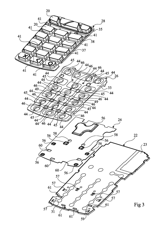
Figs. 2, 3, and 4 respectively are a general perspective
view, an exploded three-quarter top view and an exploded three
quarter bottom view of an embodiment of some internal elements of
reader 10 of Fig. 1. Reader 10 contains a printed circuit 22 on
which electronic components are connected, only a few electronic
components being shown in Fig. 3. Printed circuit 22 comprises a
surface 23 partially covered with a protection device 24 which will
be described in further detail hereafter. In the present embodi-
ment, protection device 24 is covered with a spacer 26 behaving
as a light diffuser. Spacer 26 is covered with a flexible
membrane 28 forming a keyboard, at the level of which keys 20
are formed. Keyboard membrane 28 comprises nineteen keys 20.
CA 02719037 2010-09-20
7
Printed circuit 22 comprises conductive tracks, not
shown, for example, made of copper, on the side of surface 23.
Only some locations of conductive tracks of printed circuit 22
forming switches of power supply contact areas have been shown
in the form of ellipses 31. A switch corresponds, for example,
to the different ends of two conductive tracks which correspond,
for example, to interdigitated combs. A power supply contact
area corresponds, for example, to a comb.
Spacer 26 comprises an upper surface 33 covered with
keyboard membrane 28 and a lower surface 34 resting on protection
device 24. According to the present embodiment, surfaces 33 and 34
are not parallel and form an angle of a few degrees, for example
ranging between 10 and 20 , preferably between 2 and 6 .
Keyboard membrane 28, for example made of silicone or
polyurethane, comprises a base 35 having a surface 36 resting on
spacer 26 and a surface 37 oriented towards upper package
portion 14. Each key 20 has a substantially parallelepipedal
shape and is connected to base 35 by a thinned-down upper lip
38. Further, each key 20 in continued on the side of surface 36
by a pin 40 which projects substantially perpendicularly to the
plane of base 35. Keyboard membrane 28 further comprises pins 41
which project from surface 36 substantially perpendicularly
thereto and which are connected to base 35 by a thinned-down
peripheral lip 42. Keyboard membrane 28 also comprises lugs 43
distributed on surface 36 of base 35. The length of pins 40, 41
is not uniform. More specifically, the length of pins 40, 41
increases along with the thickness of the portion of spacer 26
located close to the considered pins. In the present embodiment,
keyboard membrane 28 comprises nineteen pins 40, eight pins 41,
and ten lugs 43.
Spacer 26 is crossed by nineteen cylindrical openings
44 intended to receive pins 40 of keyboard membrane 28 and eight
cylindrical openings 45, of same diameter or of smaller diameter
than openings 44 and intended to receive pins 41. Further,
spacer 26 is crossed by ten cylindrical openings 46 of smaller
CA 02719037 2010-09-20
8
diameter intended to receive lugs 43. In the present embodiment,
openings 44, 45, 46 have axes perpendicular to surface 33 of
spacer 26. Spacer 26 comprises through openings 49 intended for
the passing of elements of reader 10, for example, means for
fastening package 12. Spacer 26 comprises non-through recesses
50, 51 on the side of surface 34.
Figs. 5 and 6 show more detailed perspective views of
protection device 24. Reference numeral 53 is used to designate
the surface of protection device 24 in contact with spacer 26
and reference numeral 54 is used to designate the surface of
protection device 24 covering printed circuit 22. Surface 53
cannot extend under the entire surface 33 of spacer 26. In par-
ticular, the peripheral shape of protection device 24 may enable
the passing of electronic components connected to surface 23 of
printed circuit 22.
Protection device 24 has a resilient structure. It is
capable of being locally deformed and takes, in the absence of
external action, a generally planar shape except for indenta-
tions 56 which project on the side of surface 53. Each indenta-
tion 56 is arranged at the level of one of recesses 50 of spacer
26 and may have a shape substantially complementary to the asso-
ciated recess 50. Each indentation 56 may be obtained by plastic
deformation of protection device 24. Electronic components 57
may be provided on printed circuit 22 at the level of at least
some of indentations 56 of protection device 24.
Through openings 58, 60 may be provided in protection
device 24. More specifically, each opening 58 is provided
substantially as an extension of one of openings 49 of spacer 26
and is intended to enable the passing of elements of the reader,
for example means for fastening upper and lower package portions
14, 16. Openings 60 are provided substantially as an extension
of recesses 51 of spacer 26 and are intended to enable the pass-
ing of light-emitting diodes 61 connected to surface 23 of
printed circuit 22.
CA 02719037 2010-09-20
9
Protection device 24 comprises, on the side of surface
54, planar conductive lands 66, for example, made of carbon, for
each of keys 20. Protection device 24 further comprises, on the
side of surface 54, domed conductive elements 68A and 68B,
called domes. Each dome 68A, 68B is associated with a pin 41.
Domes 68A and 68B have slightly different structures, as will be
described in further detail hereafter.
Figs. 7 to 12 show partial simplified cross-section
views of the stack formed by printed circuit 22, protection
device 24, spacer 26, and keyboard membrane 28 at the level of a
carbon land 66, of a dome 68A, and of a dome 68B. In the draw-
ings, the ratios between dimensions are not kept with respect to
the preceding drawings. According to the present embodiment,
protection device 24 is a flex circuit formed of a substrate 78
made of a resilient material, for example, a thermoplastic resin
such as polyethylene therephtalate (PET) having a thickness, for
example, on the order of 0.1 mm. One or several conductive
tracks 80 are formed on substrate 78 on the side of printed
circuit 22. Tracks 80 are, for example, made of silver ink and
are obtained by serigraphy. Tracks 80 and substrate 78 are cov-
ered with a varnish layer 92, for example, formed of a dielec-
tric material. A stack 93 of three layers 94, 96, and 98,
forming a separator, covers varnish layer 92. Separator 93 has,
for example, a thickness on the order of 0.2 mm. It is possible
for separator 93 not to be present at the level of each indenta-
tion 56. Spacer 26 may be held on protection device 24 via a
gluing material 99. Separator 93 comprises an opening 100 at the
level of each switch or power supply contact area 31. For Figs.
7 to 10, a switch 31 has been shown in the form of two separate
conductive tracks 101, 102 formed on printed circuit 22 substan-
tially at the level of opening 100 of separator 93 and, for
Figs. 11 and 12, a power supply contact area 31 has been shown
in the form of a conductive track 103.
Figs. 7 and 8 are cross-section views at the level of
a conductive land 66 respectively in the absence of any action
CA 02719037 2010-09-20
on key 20 and when key 20 is pressed. Carbon land 66 covers var-
nish layer 92 and opening 100 of separator 93 at least partially
exposes carbon land 66. As appears in Fig. 8, when key 20 is
pressed, lip 38 deforms to enable the key to move down along an
5 axis D substantially perpendicular to surface 33. Pin 40 causes
a local deformation of protection device 24 along axis D'
perpendicularly to surface 34 at the level of opening 100 of
separator 93 so that carbon land 66 comes into contact with
tracks 101 and 102 and provides an electric connection between
10 the tracks. When no further pressure is exerted on key 20,
protection device 24 resiliently returns to its neutral position
in which it takes a planar configuration at the level of pin 40,
land 66 being then separated from conductive tracks 101, 102.
Figs. 9 and 10 are cross-section views at the level of
a conductive dome 68A respectively in the absence and in the
presence of upper package portion 14. Dome 68A is a metal part
having, for example, a 0.05-mm thickness corresponding, for
example, to a portion of a sphere or of an ellipsoid. Dome 68A
is formed, for example, by deformation of a spring steel plate.
The peripheral edge of dome 68A may be located in a housing 110
provided in separator 93. When upper package portion 14 is
arranged, a finger 112 provided at the level of the internal
surface of upper package portion 14 bears against pin 41, which
is displaced and bears against dome 68A. Dome 68A deforms to
come into contact with conductive tracks 101, 102, creating an
electric contact between them. The deformed state of dome 68A
corresponds to an unstable position thereof so that, as soon as
the action of finger 112 on pin 41 stops, dome 68A takes back
its domed shape and breaks the electric contact with tracks 101,
102.
Fig. 11 is a view similar to Fig. 9 at the level of a
dome 68B. As compared with what has been previously described in
relation with Fig. 9, varnish layer 92 comprises an opening 113
which exposes one or several sections of track 80 substantially
at the level of dome 68B. Thereby, when flex circuit 24 and dome
CA 02719037 2010-09-20
11
68B are deformed under the action of pin 41, dome 68B comes into
contact, on the one hand, with track 80 and, on the other hand,
with track 103 of printed circuit 22. Such a contact is used to
supply track 80. The deformed state of dome 68B corresponds to
an unstable position thereof so that, as soon as the action of
finger 112 on pin 41 stops, dome 68B takes back its domed shape
and breaks the electric contact between track 103 and track 80.
Fig. 13 is a bottom view of protection device 24 show-
ing an example of distribution of conductive tracks 80 on
substrate 78. Domes 68A and 68B have been shown in the form of
circles. In the present example, a single track 80 extends on
substrate 78. Track 80 comprises a first end pad 104 at the
level of one of domes 68B and a second end pad 105 at the level
of the other dome 68B. Track 80 substantially zigzags across the
entire surface of protection device 24. In particular, track 80
extends at the level of domes 68A and of conductive lands 66,
not shown. Conductive track 80 also extends at the level of
indentations 56.
Preferably, the section of track 80 brought by deform-
able dome 68B into contact with a conductive track 103 of
circuit 22 corresponds to an end of track 80. Thus, both ends of
track 80 are connected to conductive portions of deformable
regions (domes 68B) of the protection device.
Although this is not clearly shown in Figs. 11 and 12,
deformable conductive region 68B is only in contact with the end
point of track 80 by an opening through insulating layer 92.
Indeed, it is not desirable for the contact to short-circuit
several sections since this risks to "blind" some areas of the
protection device and then to adversely affect the reliability
of the detection.
To avoid a pirate supply of track 80, domes 68B for
supplying track 80 (and thus end pads 104 and 105) are placed
outside of the periphery of the protection device. Thus, conduc-
tive track 80 protects not only against an intrusion attempt by
means of a probe or the like, but also against a displacement of
CA 02719037 2010-09-20
12
the system. The corresponding detections are performed by one or
several adapted electronic circuits, supported by the printed
circuit.
The width of conductive track 80 may be variable but
preferably remains much lower (preferably, by a factor greater
than 5) than the diameter of a dome. The narrower track 80 and
the lower the intervals between sections, the better the sensi-
tivity of the detection device. Further, the pattern followed by
track 80 may take different shapes (coils, combs, curved sec-
tions, etc.) . In the case where several tracks 80 are provided,
they may be supplied by same deformable regions of the protec-
tion device and corresponding tracks of the printed circuit, or
be associated with different deformable regions.
Fig. 14 is a view similar to Fig. 2 in which a cross-
section has been made. Lugs 43 of keyboard membrane 28 are held
in the corresponding openings 46 of spacer 26 and hold keyboard
membrane 28 in position with respect to spacer 26.
The present embodiment enables to prevent the access
to metal tracks 101, 102 of printed circuit 22 while preserving
the switch function of pins 40, 41.
The present embodiment enables to protect some elec-
tronic components 57 present on printed circuit 22 against an
intrusion by encapsulating these components 57 with protection
device 24.
In the present embodiment, the two surfaces 33, 34 of
spacer 26 may be tilted with respect to each other and not
parallel. Spacer 26 enables to tilt the displacement axes of
keys 20 of the keyboard with respect to the displacement axes of
the deformable portions of protection device 24. Keys 20 can
thus be oriented to obtain the simplest and most natural possi-
ble motions for a user.
In the present embodiment, for each key 20, protection
device 24 is planar in the absence of an external action and is
deformed to provide the electric connection between conductive
land 66 and conductive tracks 101, 102. The travel of protection
CA 02719037 2010-09-20
13
device 24 is on the order of 1 mm. The switching speed is thus
privileged. For pins 41, protection device 24 has, in the
absence of an external action, a domed shape due to resilient
conductive element 68A and is deformed to provide the electric
connection between conductive element 68A and conductive tracks
101, 102.
Specific embodiments of the present invention have
been described. Various alterations and modifications will occur
to those skilled in the art. In particular, it may be provided
to associate with keys 20 of keyboard membrane 28 the structure
of protection device 24 shown in Figs. 9 and 10 where protection
device 24 comprise a resilient conductive element 68A having a
domed shape in the absence of an external action. In this case,
when key 20 is pressed, pin 40 continuing key 20 deforms conduc-
tive element 68A to provide the electric connection between
conductive tracks 101, 102 of printed circuit 22. Further, a
protection device in which membrane 28 would be used as a
substrate for track 80 and where conductive lands 66 and domes
68A and 68B would be directly placed on membrane 28, may be
envisaged. Further, the resilient function of domes 68A and 68B
may be achieved by thermoforming of protection device 24 above
areas 31.