Note: Descriptions are shown in the official language in which they were submitted.
CA 02719584 2010-09-23
WO 2009/120832 PCT/US2009/038352
DC BUS VOLTAGE HARMONICS REDUCTION
Cross-reference to related applications
[001] The application claims the benefit of U.S. Application Serial Number
12/057,856. filed March 28, 2008, the contents of which is incorporated herein
in its entirety.
Backaound
[002] This invention relates to power conversion systems that generate
regulated direct current (DC) bus voltages from an alternating current (AC)
power supply.
[003] Electricity generated by power plants is delivered via utility grids to
power consuming facilities in the form of three-phase alternating current.
However, AC power is not always suitable for end use and sometimes needs to
be converted into usable forms (e.g., DC) before being connected to a load. In
such case, an AC/DC converter is used. In general, an AC/DC converter
receives AC power at its input terminal and outputs DC power at its DC link.
To produce satisfactory outputs, an AC/DC converter is often operated with a
controller, which regulates the waveform and magnitude of DC bus voltage at
a desired level.
[004] Among various types of AC/DC converters, one in particular - Pulse
Width Modulation (PWM) controlled AC/DC converters - has gained
increasing popularity in the past decade. PWM AC/DC converters offer
several advanced features over traditional converters, such as sinusoidal
input
current at unity power factor and high quality output voltage at the DC bus.
Therefore, PWM converters can be used in a wide range of applications,
including magnet power supplies, DC motor drives, and utility interactive
photovoltaic systems.
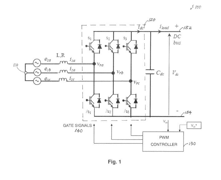
[005] One example of a PWM AC/DC converter is shown in Fig. 1. In this
example, an AC/DC converter 100 receives at an input terminal 110 an AC
power including three-phase voltage inputs esa, eb, and e, each having a
differential phase of 1200 from the others. Current inputs isa, isb, and i,
also in
AC waveforms, flow through selected lines into a switching circuit 120 in the
converter 100. The switching circuit 120 has six switching devices (e.g.,
diodes, bipolar junction transistors, etc) arranged in pairs, including S1,
/S1,
-1-
CA 02719584 2010-09-23
WO 2009/120832 PCT/US2009/038352
S2, /S2, S3 and /S3 as shown in the figure. Each pair of switching devices is
associated with one phase of the AC power, and their duty cycles in
combination define the waveform and magnitude of output voltage Vdc. A
PWM controller 130 controls a set of gate signals 140 for opening and closing
the switching devices in specific sequences, so that a substantially constant
voltage Vdc can be maintained at a prescribed level Vdc * across positive and
negative DC buses 152 and 154.
[006] Several control schemes exist for DC bus voltage regulation. In most
cases, the controller 130 detects an error between the actual and prescribed
voltage levels and drives the switching devices with controlled PWM gate
signals sufficient for compensating the error. In some cases, a larger DC link
capacitor 140 may also be used across DC buses to help maintain the output
voltage at the desired level. By reducing voltage distortion and current
ripple,
PWM controlled AC/DC converters can provide high quality voltage output at
the DC link.
[007] However, such performance is not necessarily guaranteed under
unbalanced input voltage conditions, which may occur in real systems for
many reasons. For example, nonlinear loads, nonsymmetrical transformer
windings or transmission impedances in the circuit, and accidental shorting of
one phase to the ground could all lead to unequal drop/rise of voltage
amplitudes in three phases and result in unbalanced input conditions.
[008] Regardless of the cause, one common characteristic of unbalanced
input voltage conditions is the appearance of negative-sequence component in
the input. Negative-sequence component causes even harmonics in the DC
link voltage and odd harmonics in the converter current, which can
significantly deteriorate the quality of DC power supplied to the load. Under
extreme conditions, it may even lead to a system trip if maximum DC bus
voltage is exceeded. In large power conversion systems, these problems can
grow in severity as the number of converters connected to a common AC link
increases.
Summary
[009] In one aspect, in general, the invention features a control system
configured for use with a three-phase PWM converter. The control system
receives an input signal from a three-phase power supply and provides an
output signal at a DC link. A voltage-separating module generates on the
- 2-
CA 02719584 2010-09-23
WO 2009/120832 PCT/US2009/038352
basis of the input signal a positive sequence voltage component and a negative
sequence voltage component in a rotating reference frame. A reference
current computation module uses at least the positive sequence voltage
component and the negative sequence voltage component to compute a first
reference current and a second reference current. A current regulating module
uses at least the first reference current and the second reference current to
generate a command signal. The command signal is provided to a driving
circuit of the three-phase PWM converter for generating a regulated DC bus
voltage at the DC link.
[010] Embodiments may include one or more of the following features.
[011] The input signal includes an input voltage signal and an input current
signal.
[012] A voltage detection circuit provides a first, a second, and a third
phase
input voltage component to the voltage-separating module on the basis of the
input voltage signal.
[013] A three phase to two phase voltage transformer generates two phase a
and 0 axis voltage components on the basis of the first, second and third
phase
input voltage components. A stationary to rotating reference frame voltage
converter generates rotating d and q axis voltage components in the rotating
reference frame on the basis of the a and 0 axis voltage components. The
rotating reference frame has a phase determined by an angle signal.
[014] A phase locked loop generates the angle signal on the basis of a
selected one of the rotating d and q axis sequence components.
[015] The rotating d axis sequence component includes a positive and
negative d axis sequence component. The rotating q axis sequence component
includes a positive and negative q axis sequence component.
[016] A current detection circuit provides a first, a second, and a third
phase
input current component on the basis of the input current signal.
[017] A three phase to two phase current transformer generates two phase a
and 0 axis current components on the basis of the first, second, and third
phase
input current components. A stationary to rotating reference frame current
converter generates rotating d and q axis current components in the rotating
reference frame on the basis of the a and 0 axis current components.
- 3-
CA 02719584 2010-09-23
WO 2009/120832 PCT/US2009/038352
[018] A DC link voltage detection circuit provides a DC bus voltage signal
on the basis of the output signal at the DC link.
[019] A DC link voltage regulator receives a pre-determined DC bus
reference voltage signal for generating a DC bus reference current signal on
the basis of the DC bus voltage signal.
[020] The reference current computation module uses the DC bus reference
current signal to compute the first reference current and the second reference
current. The first reference current includes a rotating d axis reference
current.
The second reference current includes a rotating q axis reference current.
[021] A d-axis current regulator generates a first correction voltage signal.
A
q-axis current regulator generates the second correction voltage signal. A
first
summer provides a first reference voltage on the basis of the first correction
voltage signal. A second summer provides a second reference voltage on the
basis of the second correction voltage signal. The first and second reference
voltages are used for generating the command signal.
[022] The DC link voltage regulator includes a proportional integral
regulator.
[023] The d-axis current regulator includes a proportional integral regulator
and may further include an infinite sine gain unit.
[024] Similarly, the q-axis current regulator includes a proportional integral
regulator and may further include an infinite sine gain unit.
[025] The DC link voltage detection circuit further includes a low pass
filter.
[026] Among other features and advantages, the invention provides a control
system for reducing 2"d order DC bus voltage harmonics caused by
unbalanced input voltages. By eliminating input current distortion and voltage
fluctuation at the DC bus, stability of an AC/DC power converter can be
improved. In addition, since it is computationally simple to regulate both
positive- and negative-sequence current components in the same synchronous
reference frame, such control system can be easily integrated with
conventional AC/DC power converters. Moreover, when used in large-
capacity power systems, e.g., a motor control center having multiple motor
drives connected on a common DC bus, satisfactory voltage performance may
be achieved without increasing DC bus capacitance, thereby minimizing
overall system cost.
- 4-
CA 02719584 2010-09-23
WO 2009/120832 PCT/US2009/038352
[027] Other features and advantages of the invention are apparent from the
following description, and from the claims.
Description of Drawings
[028] FIG. 1 is a conventional AC/DC power conversion system controlled
by PWM gate signals.
[029] Fig. 2 is a block diagram of a control system for reducing DC bus
voltage harmonics.
[030] Fig. 3 is a flow chart of the control scheme used in the control system
illustrated in Fig. 2.
[031] Figs. 4A to 4C are illustrative plots of AC-line voltage, DC link
voltage, converter line current, respectively.
[032] Fig. 5 is a diagram of the reference current computation module used
in Fig. 2.
[033] Fig. 6 is a diagram of the current regulator used in Fig. 2.
[034] Fig. 7 is a diagram of the infinite sine gain used in Fig. 6.
Detailed Description
[035] Referring to Fig. 2, an AC/DC power conversion system 200 includes
an AC/DC converter 220 coupled between a three phase power supply 210 and
a DC load 230. The AC/DC converter 220 operates in a PWM mode to
convert alternating current provided by the power supply 210 at AC line 260
to direct current at DC link 270 to supply the load 230. For the reasons
discussed above, unbalanced input voltage conditions may occur and cause 2d
order harmonics in output voltage at the DC link 270, which can affect
converter performance and system stability. Therefore, a PWM control system
280 is used in conjunction with the converter 220 for controlling DC bus
voltage under unbalanced input conditions. In particular, 2d order harmonics
at the DC link 270 is desired to be regulated.
[036] The control system 280 includes a voltage sample and hold circuit
202, which samples AC line input voltage and provides digitized three-phase
voltage signals ea, eb, and e, to a three phase to two phase transformer 204.
The transformer 204 transforms three phase signals into two phase quantities
- 5-
CA 02719584 2010-09-23
WO 2009/120832 PCT/US2009/038352
in a stationary a-,,8- coordinate system. The output of the transformer 204
(i.e., ea and efi) is converted by a stationary to rotating reference frame
converter 206 to d- and q- axis components (i.e., ed and eq) in a rotating
reference frame defined by a phase angle 0. In this rotating reference frame,
positive and negative sequence components ei, edn, eq , eqn of the voltage
signals ed and eq are also obtained, whereas non-zero values of negative
sequence components edn and eqn indicate the presence of unbalanced voltage
conditions.
[037] Next, positive and negative voltage components ei, edn, eq and eqn are
delivered to a reference current computation module 240 for computing
reference current signals id * and iq *. Another input signal used by the
reference current computation module 240 is a DC bus reference current
signal ide*, provided by a DC link voltage regulator 238. DC link voltage
regulator 238 is used for regulating DC bus voltage Vde to a pre-determined
level Vde * 236, and accordingly, its output id, * represents the current
level
required at the DC bus for this purpose. A voltage sample and hold circuit 232
samples actual DC bus voltage Vde7 which is sometimes filtered by a low pass
filter 234 before reaching the DC link voltage regulator 238.
[038] Using id,* and the four voltage components, the reference current
computation module 240 outputs reference current signals id* and iq* to a
current regulator 250, which then compares actual input current signals id and
iq with references id* and iq* to determine error signals ide and iqe,
respectively.
Like input voltage signals ed and eq, input current signals id and iq are
obtained
from AC line 260 via a current sample and hold circuit 212, a three phase to
two phase transformer 214, and a stationary to rotating reference frame
converter 216.
[039] The current regulator 250 includes a d- axis regulator 252 and a q- axis
regulator 254, in which correction voltages ede and eqe sufficient for
correcting
current errors ide and iqe are computed, respectively. Correction voltages ede
and eqe are then summed with input voltage signals ed and eq (previously
generated by converter 206) in summers 226 and 228 to obtain reference
voltage signals Vd and Vq, which ultimately determines gate signals for the
converter 220 and the level of current that needs to be injected to the DC
bus.
[040] Upon receiving reference voltages Vd and Vq, a rectangular to polar
converter 224 converts these d- and q- axis components into magnitude M and
phase angle 0 in a polar coordinate system, and sends them to a space vector
- 6-
CA 02719584 2010-09-23
WO 2009/120832 PCT/US2009/038352
reference generator 222. Using M and 0, the space vector reference generator
222 computes PWM gate signals and drives the switching devices in the
converter 220 with duty cycle arrangements sufficient for achieving the
desired DC bus voltage Vdc*. For example, if the actual DC bus voltage Vdc is
found to be lower than the desired level Vdc*, PWM gate signals will adjust to
changes in duty cycle arrangements so that additional current is injected into
DC bus to raise the magnitude of Vdc.
[041] Note in the current regulator 250, both negative and positive sequence
current components are regulated simultaneously in the same synchronous
reference frame. Thus, to ensure that the rotating reference frame of id and
iq
(created in converter 216) is consistent with that of id* and iq * (created in
converter 206), a phase locked loop 208 is used to lock both d-, q- coordinate
systems to the same synchronous reference frame angle 0 218. In this
example, the reference frame angle 0 is determined based on d- axis positive
sequence component el, since positive sequence component often has a
greater magnitude than negative sequence component therefore is easier to
implement the phase lock. However, in some other examples, it is also
possible to lock phase on the negative sequence, e.g., edn or eqn.
[042] Referring to Fig. 3, the logics and functions of several control modules
used in the above converter system 200 are further illustrated in a flow chart
300. Initially, in step 302, three phase voltages signals ea, eb, and e,
retrieved
by the voltage hold and sample circuit 202 are transformed into two phase
stationary a-,,8- coordinates using Clark Transformation, as given by:
where ea and e,8 are the input voltage signals projected on the stationary a-,
/1-
coordinate system.
[043] In step 304, positive and negative sequence voltage components are
decomposed from ea and e,8. There are many ways of decomposing the voltage
components. In one example, the positive and negative sequences are
obtained as:
t T.
4
T
4 (2)
T
t3=-it'õ(r1 t-
4
T.
4
- 7-
CA 02719584 2010-09-23
WO 2009/120832 PCT/US2009/038352
where T represents the period of AC signal, e.g., 1/60 sec in a common AC
line voltage. Here, non-zero values of negative sequence components can and
e/3 indicate the occurrence of unbalanced input conditions.
[044] In a next step 306, each sequence component is represented in a
rotating reference frame along its d- and q- axis, based on unit Park
Transformation, as given by:
+
where 0) represents the rotational speed of the rotating frame (e.g., in
rad/s),
and the reference frame angle 0 is calculated as 9=cot.
[045] As discussed above in the control system 200, positive and negative d-
q- voltage components are fed into the reference computation module 240 for
computing reference current signals id * and iq *, which are the desired d-
and
q- axis current components for maintaining DC bus voltage at Vde*. The
computation, as illustrated in step 330, is based on the equations of power
flow control:
, ,.,r (4)
is t -(': )'I
!~ 1 ( f't. - f"der ` Dili:
where id,* is determined by a DC link voltage regulator in step 316 to be the
desired/reference DC bus current for achieving Vde*. Examples of DC link
voltage regulators include commonly used PI controllers, which are known to
be used for eliminating steady state error in output signals. In some
examples,
prior to step 316, actual DC bus voltage signal Vde is first processed in step
314 by a low pass filter to eliminate certain harmonics from its waveform,
which may otherwise interfere with the determination of id, * in the voltage
regulator.
[046] Upon collecting the reference current signals id* and iq*, in step 340,
the current regulator compares id* and iq* with sampled AC line current
components id and iq for generating d- and q- axis correction voltages ede and
- 8-
CA 02719584 2010-09-23
WO 2009/120832 PCT/US2009/038352
eqe, respectively. The conversion of id and iq from three phase signals ia,
ib, and
ie follows a similar set of Clark Transformation 324 and Park Transformation
326 to those described for voltage conversion. Note in this step, both
positive
current sequences i1', iq and negative current sequences id", iqn are
regulated
together to the reference levels id* and iq* in the same positive synchronous
reference frame. Examples of the current regulator will be described in
greater
details later.
[047] In a following step 350, correction voltages ede and eqe are added to
actual line voltage ed and eq to generate reference voltages Vd and Vq, which
allows the space vector generator to compute desired command duty cycles for
the switching devices in the converter 220. In a final step 360, PWM gate
signals corresponding to the closing and opening sequence of each pair of
switching devices are determined and sent to the AC/DC converter.
[048] Referring to Figs. 4A to 4C, for the exemplary control system 280
described in Fig. 2, simulation results of AC line voltage, DC link voltage,
and
converter input current are shown, respectively. As illustrated in Fig. 4A,
voltage supply at the AC line has three sinusoidal waveforms 402 (ea), 404
(eb), and 406 (ee) having a differential phase of 120 from each other. In a
common 60Hz system for example, each waveform has a cycle "T" of
0.0167s. Thus, ea leads eb by 0.056s (i.e., T/3) and e, by 0.11s (i.e., 2T/3).
Note the amplitude of ee is simulated to be only at 50% of the level in ea and
eb, thereby creating an unbalanced input condition. Without proper control,
such unbalance in AC line voltage causes 2' order (120Hz) harmonics in DC
bus voltage 410, which further causes distortion in converter input current
waveforms 422, 424, and 426, as shown in Figs. 4B and 4C, respectively.
[049] To demonstrate the effect of control system 280, at t = 0.025s, control
circuit is activated. Following the activation, as shown in Fig. 4B, DC link
voltage quickly adjusts from its original waveform 410 to a post-control
waveform 410' in response to the power flow control. After a transient period
of - 0.005s, no 2' order harmonic content can be observed in steady state DC
link voltage 410' . Meanwhile, distortions formerly present in converter line
current waveforms 422, 434, 426 are also eliminated from steady state
waveforms 422', 424', and 426', as shown in Fig. 4C. Unlike DC link voltage
or converter line current, AC line input voltage is usually not controlled,
thus
its original waveforms 402, 404, and 406 are not affected, as shown in Fig.
4A.
- 9-
CA 02719584 2010-09-23
WO 2009/120832 PCT/US2009/038352
[050] Having illustrated the overall control scheme of the PWM control
system 280 as well as its voltage regulating effect, several internal modules
employed in the control loop are described in greater details below.
[051] Referring to Fig. 5, an example of the reference current computation
module 240 is shown. A current input of the reference current computation
module 240, i.e., reference DC bus current id,*, is multiplied by each of four
voltage inputs, including positive sequence components el and eq and
negative sequence components edn and eqn, in one of four multipliers 512, 514,
516, and 518, respectively. The scalar outputs of the first two multiplier 512
and 514, indicating the positive sequence power flows along d- and q- axis,
are converted by a scalar-vector converter 522 into a positive sequence power
flow ve torp of * . Likewise, the scalar outputs of multiplier 516 and
518 are c9nv ~ed:l y a second scalar-vector converter 524 into a negative
sequence power flow vector
e,'11"'
* e 4 n old , . A summer 526 then sums the positive sequence power flow vector
with the inverted negative sequence power flow vector, and outputs a
reference current vector
i*
d
representing d- and q- axis reference current id * and iq *, as defined by
9
equa ion (4) described earlier.
[052] Referring to Fig. 6, an example of the current regulator 250 is shown in
greater details. Inputs to the current regulator 250, including q- axis
reference
and sampled current components 602 and 604 (i.e., iq* and iq) and d- axis
reference and sampled current components 606 and 608 (i.e., id* and id) are
processed in a q- axis current regulator 610 and a d- axis current regulator
650,
respectively. Serving as a proportional integral (PI) regulator in essence,
each
current regulator determines an error between its two input signals and
outputs
a correction signal for eliminating the error.
[053] For example, in the q-axis regulator 610, iq * and iq are first received
at
a positive and negative input terminal of a summer 612, which outputs the
error between the reference and sampled q-axis current components, i.e., iqe,
in
an error signal 614. Next, the error signal 614 flows along signal lines 615,
613, and 617 in parallel and is processed in an integral regulator/integrator
630, a proportional regulator/multiplier 624, and an infinite sine gain 700,
respectively, before regulator 610 outputs the correction signal, i.e., q-axis
correction voltage eqe.
-10-
CA 02719584 2010-09-23
WO 2009/120832 PCT/US2009/038352
[054] The integrator 630 integrates in a discrete time domain the error signal
614 multiplied by an integral gain KI 616. That is, the output of the
integrator
630 at any clock time t, (i.e., X(tn)), is equal to the output at a previous
clock
time tn_I (i.e., >X(tn_j)), plus K1 times the error signal 614, as given by:
n-1
X(t) X(t1)+K1 (i; (tn) - iq (tn )) (5)
0
To implement this integrator, a unit delay element 636 is used. The first
input
634 of the unit delay element 636, i.e., Pcarrier, is a system clock signal.
By
feeding back the output signal 642 to its input through a summer 632, error
signal is integrated at a clock signal pulse. This integral output 642 is then
provided to a four-input summer 640 as a first input signal.
[055] A second input signal 644 of the summer 640 is the proportional output
of the error signa1K61(4, vhi5h is simply the error signal multiplied by a
proportional gain 618 q Kp, as given by
[056] A third input signal 646 of the summer 610 is coupled to an output of
an infinite sine gain unit 700, the internals of which is also shown in Fig.
7.
Infinite sine gain unit in general functions as an undamped oscillator having
a
substantially infinite gain at a predetermined frequency 710. That is, in
response to any finite input 720, the output signal at the predetermined
frequency 710 increases in proportion to time without limit. This
characteristic
is determined by the following transfer function T(s), as given by:
s
T(s)= 2+~2 (6)
S 0
where s = a +j co, a complex variable in Laplace domain, and coo is a
predetermined frequency. The magnitude of the transfer function T(s) at an
input frequency of co=coo can be obtained by simply replacing the variable s
with jcoo, as given below:
T( (;
q) = V C)2 + Cf~2 (7)
With the denominator equal to zero, this unit has an infinite gain
at coo.
[057] In the context of the q- axis regulator 610 as shown in Fig. 6, the
infinite sine gain unit 700 receives a frequency signal 710 that sets the
frequency to which this unit 700 is tuned, and outputs a signal 646
representing an input 720 signal at this tune frequency. Here, by fixing the
frequency signal 710 at 120/Fcarrier, i.e., twice the frequency of supply
voltage divided by system sampling rate, 120Hz AC component (i.e., 2d order
- 11-
CA 02719584 2010-09-23
WO 2009/120832 PCT/US2009/038352
harmonics) in the current error signal 614 is tracked and provided to the
summer 640. As previously discussed, negative sequence component appears
as 120Hz AC component in the positive synchronous frame. Thus, this infinite
sine gain unit 700 allows the negative sequence component to be regulated in
the same positive synchronous frame as positive sequence component is being
regulated by the proportional-integral part (630 and 624) of the current
regulator 610.
[058] Now with three summer input signals 642, 644, and 646 described as
being only associated with q- axis current components, the fourth input signal
648 of the summer 640 reflects the cross coupling between d- and q- axis
current components. For example, the influence of a d- axis current
component on the q- axis regulator can be described by the following
relationship:
V/C = 27LOf ILPid * (8)
where VqC is the cross coupling term provided as the fourth input to the
summer 640, 2zf is the radian frequency of supply voltage (i.e., 2Z*60Hz), L
is the inductance between the converter and harmonic filters across which the
feedback voltage is sensed (e.g., at the three phase power supply), and id* is
the d-axis reference current component. Numerical values of L and 2zf are
provided as inputs 686 and 688 to a multiplier 684, which subsequently
outputs the cross coupling term 648 to the summer 640.
[059] Having described the q- axis current regulator 610, by which both
positive and negative q- axis sequence components are regulated, its
counterpart - d- axis current regulator 650 will be described briefly below.
Again, in order to regulate both positive and negative d- axis sequence
components in the same synchronous reference frame, an integral
regulator/integrator 660, a proportional regulator/multiplier 656, and an
infinite sine gain unit 700 are implemented in the circuit to provide output
signals 672, 674, and 676 to a summer 670, respectively. Note here, a fourth
inverting input 678 of the summer 670, representing the cross coupling of q-
axis current component on the d- axis regulator 650, is defined as:
VdC = -27rOf OLD=q * (9)
- 12-
CA 02719584 2010-09-23
WO 2009/120832 PCT/US2009/038352
where Vd' is the cross coupling term, iq * is the q- axis reference current
component, with f and L same as described before. Other units in the d- axis
regulator 650 function in a similar way as described in q- axis regulator 610.
[060] Therefore, in the current regulator 250, d- axis and q- axis current
signals are regulated in a d- axis and q- axis regulator, respectively, in
which
both positive and negative sequence components are processed in the same
synchronous reference frame.
[061] Referring to Fig. 7, an example of the infinite sine gain unit 700 used
in the current regulator 250 is shown in greater detail. Internals of the
infinite
sine gain unit 700 are further described in U.S. Patent Application Serial No.
6,977,827 B2 by Gritter, the disclosure of which is incorporated herein by
reference. In addition, examples of three phase to two phase transformers 204
and 214, stationary to rotating reference frame converters 206 and 216, phase
locked loop 208, and DC link voltage regulator 238 are also described in U.S.
Patent Application Serial No. 6,977,827 B2 by Gritter. It will be appreciated
by those of ordinary skill in the art that various forms of circuits may be
used
in these modules for similar functions.
[062] It is to be understood that the foregoing description is intended to
illustrate and not to limit the scope of the invention, which is defined by
the
scope of the appended claims. Other embodiments are within the scope of the
following claims.
- 13-