Note: Descriptions are shown in the official language in which they were submitted.
CA 02719645 2010-09-24
WO 2009/120610 PCT/US2009/037881
ELECTROMECHANICAL DEVICE WITH SPACING LAYER
BACKGROUND
[0001] Electromechanical systems (MEMS) include mechanical elements,
actuators, and electronics. Mechanical elements may be created using
deposition, etching,
and/or other machining processes that etch away parts of substrates and/or
deposited material
layers or that add layers to form electrical and electromechanical devices.
One type of
MEMS device is called an interferometric modulator. As used herein, the term
interferometric modulator or interferometric light modulator refers to a
device that selectively
absorbs and/or reflects light using the principles of optical interference. In
certain
embodiments, an interferometric modulator may comprise a pair of conductive
plates, one or
both of which may be transparent and/or reflective in whole or part and
capable of relative
motion upon application of an appropriate electrical signal. In a particular
embodiment, one
plate may comprise a stationary layer deposited on a substrate and the other
plate may
comprise a metallic membrane separated from the stationary layer by an air
gap. As
described herein in more detail, the position of one plate in relation to
another can change the
optical interference of light incident on the interferometric modulator. Such
devices have a
wide range of applications, and it would be beneficial in the art to utilize
and/or modify the
characteristics of these types of devices so that their features can be
exploited in improving
existing products and creating new products that have not yet been developed.
SUMMARY
[0002] In certain embodiments, a device comprises an electrode, a fixed
reflector,
a movable reflector comprising an electrically conductive material, wherein an
interferometric modulating cavity is defined between the movable reflector and
the fixed
reflector, the movable reflector being movable between at least a first
position, a second
position, and a third position. The device also comprises a spacing layer
positioned between
the fixed reflector and the electrode, the spacing layer providing a filtering
cavity.
[0003] In certain embodiments, a device comprises an electrode, a fixed
reflector,
a movable reflector comprising an electrically conductive material, wherein an
interferometric modulating cavity is defined between the movable reflector and
the fixed
CA 02719645 2010-09-24
WO 2009/120610 PCT/US2009/037881
reflector, the movable reflector being movable between at least a first
position, a second
position, and a third position. The device also comprises a spacing layer
positioned between
the fixed reflector and the electrode, the spacing laying being greater than
or equal to 160 nm
in thickness from a cross-sectional view of the device.
[0004] In certain embodiments, a device comprises an electrode, a first, fixed
means for reflecting' light, a second, movable means for reflecting light. The
second
reflecting means comprises an electrically conductive material, wherein an
interferometric
modulating cavity is defined between the first reflecting means and the second
reflecting
means. The second reflecting means is movable between at least a first
position, a second
position, and a third position. The device also comprises means for separating
the first
reflecting means and the electrode, the separating means providing a filtering
cavity.
[0005] In certain embodiments, a method of making a device for modulating
light
comprises forming an electrode, forming a spacing layer, forming a fixed
reflector, and
forming a movable reflector comprising an electrically conductive material. An
interferometric modulating cavity is defined between the movable reflector and
the fixed
reflector. The movable reflector is movable between at least a first position,
a second
position, and a third position. The spacing layer provides a filtering cavity.
BRIEF DESCRIPTION OF THE DRAWINGS
[0006] FIG. 1 is an isometric view depicting a portion of one embodiment of an
interferometric modulator display in which a movable reflective layer of a
first
interferometric modulator is in a relaxed position and a movable reflective
layer of a second
interferometric modulator is in an actuated position.
[0007] FIG. 2 is a system block diagram illustrating one embodiment of an
electronic device incorporating a 3x3 interferometric modulator display.
[0008] FIG. 3 is a diagram of movable mirror position versus applied voltage
for
one exemplary embodiment of an interferometric modulator of FIG. 1.
[0009] FIG. 4 is an illustration of a set of row and column voltages that may
be
used to drive an interferometric modulator display.
[0010] FIG. 5A illustrates one exemplary frame of display data in the 3x3
interferometric modulator display of FIG. 2.
-2-
CA 02719645 2010-09-24
WO 2009/120610 PCT/US2009/037881
100111 FIG. 5B illustrates one exemplary timing diagram for row and column
signals that may be used to write the frame of FIG. 5A.
[0012] FIGS. 6A and 6B are system block diagrams illustrating an embodiment of
a visual display device comprising a plurality of interferometric modulators.
[0013] FIG. 7A is a cross section of the device of FIG. 1.
[0014] FIG. 7B is a cross section of an alternative embodiment of an
interferometric modulator.
[0015] FIG. 7C is a cross section of another alternative embodiment of an
interferometric modulator.
[0016] FIG. 7D is a cross section of yet another alternative embodiment of an
interferometric modulator.
[0017] FIG. 7E is a cross section of an additional alternative embodiment of
an
interferometric modulator.
[0018] FIG. 8 is a schematic side cross-sectional view of a multi-state
interferometric modulator.
[0019] FIG. 9 is a schematic side cross-sectional view of a multi-state
interferometric modulator having a spacing layer.
[0020] FIG. 10 is a schematic side cross-sectional view of a pixel including
red,
green and blue tri-state interferometric modulators that have different
spacing layers.
[0021] FIG. 11 shows an example of reflectance spectra for a red tri-state
modulator.
[0022] FIG. 12 shows an example of combined modeled reflectance spectra for
red, green and blue tri-state modulators having different spacing layers.
[0023] FIG. 13 shows the positions of the red, green and blue colors perceived
in
FIG. 12 in the CTE 1976 diagram.
[0024] FIG. 14 shows an example of combined reflectance spectra for a display
of
a three-bit design.
[0025] FIG. 15 shows the positions of the red, green and blue colors perceived
in
FIG. 14 in the CTE 1976 diagram.
-3-
CA 02719645 2010-09-24
WO 2009/120610 PCT/US2009/037881
DETAILED DESCRIPTION OF THE PREFERRED EMBODIMENTS
[0026] The following detailed description is directed to certain specific
embodiments of the invention. However, the invention can be embodied in a
multitude of
different ways. In this description, reference is made to the drawings wherein
like parts are
designated with like numerals throughout. As will be apparent from the
following
description, the embodiments may be implemented in any device that is
configured to display
an image, whether in motion (e.g., video) or stationary (e.g., still image),
and whether textual
or pictorial. More particularly, it is contemplated that the embodiments may
be implemented
in or associated with a variety of electronic devices such as, but not limited
to, mobile
telephones, wireless devices, personal data assistants (PDAs), hand-held or
portable
computers, GPS receivers/navigators, cameras, MP3 players, camcorders, game
consoles,
wrist watches, clocks, calculators, television monitors, flat panel displays,
computer
monitors, auto displays (e.g., odometer display, etc.), cockpit controls
and/or displays, display
of camera views (e.g., display of a rear view camera in a vehicle), electronic
photographs,
electronic billboards or signs, projectors, architectural structures,
packaging, and aesthetic
structures (e.g., display of images on a piece of jewelry). MEMS devices of
similar structure
to those described herein can also be used in non-display applications such as
in electronic
switching devices.
[0027] One embodiment comprises a display adopting tri-state interferometric
modulating devices that have a high contrast ratio (CR) and a large gamut. In
such a tri-state
interferometric modulating device, a spacing layer provides better protection
against shorting
between the movable reflector and the electrodes. In one embodiment, the
spacing layer
defines a second interferometric modulating cavity that is found to provide
saturated light
over a range of light frequencies. As a result, the gamut of the display is
enhanced.
[0028] One interferometric modulator display embodiment comprising an
interferometric MEMS display element is illustrated in Figure 1. In these
devices, the pixels
are in either a bright or dark state. In the bright ("on" or "open") state,
the display element
reflects a large portion of incident visible light to a user. When in the dark
("off' or
"closed") state, the display element reflects little incident visible light to
the user. Depending
on the embodiment, the light reflectance properties of the "on" and "off'
states may be
-4-
CA 02719645 2010-09-24
WO 2009/120610 PCT/US2009/037881
reversed. MEMS pixels can be configured to reflect predominantly at selected
colors,
allowing for a color display in addition to black and white.
[0029] Figure 1 is an isometric view depicting two adjacent pixels in a series
of
pixels of a visual display, wherein each pixel comprises a MEMS
interferometric modulator.
In some embodiments, an interferometric modulator display comprises a
row/column array of
these interferometric modulators. Each interferometric modulator includes a
pair of
reflective layers positioned at a variable and controllable distance from each
other to form a
resonant optical gap with at least one variable dimension. In one embodiment,
one of the
reflective layers may be moved between two positions. In the first position,
referred to herein
as the relaxed position, the movable reflective layer is positioned at a
relatively large distance
from a fixed partially reflective layer. In the second position, referred to
herein as the
actuated position, the movable reflective layer is positioned more closely
adjacent to the
partially reflective layer. Incident light that reflects from the two layers
interferes
constructively or destructively depending on the position of the movable
reflective layer,
producing either an overall reflective or non-reflective state for each pixel.
[0030] The depicted portion of the pixel array in Figure 1 includes two
adjacent
interferometric modulators 12a and 12b (collectively referred to as
interferometric
modulators 12). In the interferometric modulator 12a on the left, a movable
reflective layer
14a is illustrated in a relaxed position at a predetermined distance from an
optical stack 16a,
which includes a partially reflective layer. In the interferometric modulator
12b on the right,
the movable reflective layer 14b is illustrated in an actuated position
adjacent to the optical
stack 16b.
[0031] The optical stacks 16a and l6b (collectively referred to as optical
stack
16), as referenced herein, typically comprise several fused layers, which can
include an
electrode layer, such as indium tin oxide (ITO), a partially reflective layer,
such as chromium,
and a transparent dielectric. The optical stack 16 is thus electrically
conductive, partially
transparent, and partially reflective, and may be fabricated, for example, by
depositing one or
more of the above layers onto a transparent substrate 20. The partially
reflective layer can be
formed from a variety of materials that are partially reflective such as
various metals,
semiconductors, and dielectrics. The partially reflective layer can be formed
of one or more
-5-
CA 02719645 2010-09-24
WO 2009/120610 PCT/US2009/037881
layers of materials, and each of the layers can be formed of a single material
or a combination
of materials.
[0032] In some embodiments, the layers of the optical stack 16 are patterned
into
parallel strips, and may form row electrodes in a display device as described
further below.
The movable reflective layers 14a, 14b may be formed as a series of parallel
strips of a
deposited metal layer or layers (orthogonal to the row electrodes of 16a, 16b)
deposited on
top of posts 18 and an intervening sacrificial material deposited between the
posts 18. When
the sacrificial material is etched away, the movable reflective layers 14a,
l4b are separated
from the optical stacks 16a, l6b by a defined gap 19. A highly conductive and
reflective
material such as aluminum may be used for the reflective layers 14, and these
strips may form
column electrodes in a display device.
[0033] With no applied voltage, the gap 19 remains between the movable
reflective layer 14a and optical stack 16a, with the movable reflective layer
14a in a
mechanically relaxed state, as illustrated by the pixel 12a in Figure 1.
However, when a
potential difference is applied to a selected row and column, the capacitor
formed at the
intersection of the row and column electrodes at the corresponding pixel
becomes charged,
and electrostatic forces pull the electrodes together. If the voltage is high
enough, the
movable reflective layer 14 is deformed and is forced against the optical
stack 16. A
dielectric layer (not illustrated in this Figure) within the optical stack 16
may prevent shorting
and control the separation distance between layers 14 and 16, as illustrated
by pixel 12b on
the right in Figure 1. The behavior is the same regardless of the polarity of
the applied
potential difference. In this way, row/column actuation that can control the
reflective vs.
non-reflective pixel states is analogous in many ways to that used in
conventional LCD and
other display technologies.
[0034] Figures 2 through 5B illustrate one exemplary process and system for
using an array of interferometric modulators in a display application.
[0035] Figure 2 is a system block diagram illustrating one embodiment of an
electronic device that may incorporate aspects of the invention. In the
exemplary
embodiment, the electronic device includes a processor 21 which may be any
general purpose
single- or multi-chip microprocessor such as an ARM, Pentium , Pentium 11 ,
Pentium III ,
-6-
CA 02719645 2010-09-24
WO 2009/120610 PCT/US2009/037881
Pentium IV , Pentium Pro, an 8051, a MIPS , a Power PC , an ALPHA , or any
special
purpose microprocessor such as a digital signal processor, microcontroller, or
a
programmable gate array. As is conventional in the art, the processor 21 may
be configured
to execute one or more software modules. In addition to executing an operating
system, the
processor may be configured to execute one or more software applications,
including a web
browser, a telephone application, an email program, or any other software
application.
[0036] In one embodiment, the processor 21 is also configured to communicate
with an array driver 22. In one embodiment, the array driver 22 includes a row
driver circuit
24 and a column driver circuit 26 that provide signals to a display array or
panel 30. The
cross section of the array illustrated in Figure 1 is shown by the lines 1-1
in Figure 2. For
MEMS interferometric modulators, the row/column actuation protocol may take
advantage of
a hysteresis property of these devices illustrated in Figure 3. It may
require, for example, a
volt potential difference to cause a movable layer to deform from the relaxed
state to the
actuated state. However, when the voltage is reduced from that value, the
movable layer
maintains its state as the voltage drops back below 10 volts. In the exemplary
embodiment of
Figure 3, the movable layer does not relax completely until the voltage drops
below 2 volts.
Thus, there exists a window of applied voltage, about 3 to 7 V in the example
illustrated in
Figure 3, within which the device is stable in either the relaxed or actuated
state. This is
referred to herein as the "hysteresis window" or "stability window." For a
display array
having the hysteresis characteristics of Figure 3, the row/column actuation
protocol can be
designed such that during row strobing, pixels in the strobed row that are to
be actuated are
exposed to a voltage difference of about 10 volts, and pixels that are to be
relaxed are
exposed to a voltage difference of close to zero volts. After the strobe, the
pixels are exposed
to a steady state voltage difference of about 5 volts such that they remain in
whatever state
the row strobe put them in. After being written, each pixel sees a potential
difference within
the "stability window" of 3-7 volts in this example. This feature makes the
pixel design
illustrated in Figure 1 stable under the same applied voltage conditions in
either an actuated
or relaxed pre-existing state. Since each pixel of the interferometric
modulator, whether in
the actuated or relaxed state, is essentially a capacitor formed by the fixed
and moving
reflective layers, this stable state can be held at a voltage within the
hysteresis window with
-7-
CA 02719645 2010-09-24
WO 2009/120610 PCT/US2009/037881
almost no power dissipation. Essentially no current flows into the pixel if
the applied
potential is fixed.
[0037] In typical applications, a display frame may be created by asserting
the set
of column electrodes in accordance with the desired set of actuated pixels in
the first row. A
row pulse is then applied to the row 1 electrode, actuating the pixels
corresponding to the
asserted column lines. The asserted set of column electrodes is then changed
to correspond
to the desired set of actuated pixels in the second row. A pulse is then
applied to the row 2
electrode, actuating the appropriate pixels in row 2 in accordance with the
asserted column
electrodes. The row 1 pixels are unaffected by the row 2 pulse, and remain in
the state they
were set to during the row 1 pulse. This may be repeated for the entire series
of rows in a
sequential fashion to produce the frame. Generally, the frames are refreshed
and/or updated
with new display data by continually repeating this process at some desired
number of frames
per second. A wide variety of protocols for driving row and column electrodes
of pixel
arrays to produce display frames are also well known and may be used in
conjunction with
the present invention.
[0038] Figures 4, 5A, and 5B illustrate one possible actuation protocol for
creating a display frame on the 3x3 array of Figure 2. Figure 4 illustrates a
possible set of
column and row voltage levels that may be used for pixels exhibiting the
hysteresis curves of
Figure 3. In the Figure 4 embodiment, actuating a pixel involves setting the
appropriate
column to -Vb;as, and the appropriate row to +AV, which may correspond to -5
volts and +5
volts, respectively. Relaxing the pixel is accomplished by setting the
appropriate column to
+Vb;as, and the appropriate row to the same +AV, producing a zero volt
potential difference
across the pixel. In those rows where the row voltage is held at zero volts,
the pixels are
stable in whatever state they were originally in, regardless of whether the
column is at +Vbias,
or -Vb;. As is also illustrated in Figure 4, it will be appreciated that
voltages of opposite
polarity than those described above can be used, e.g., actuating a pixel can
involve setting the
appropriate column to +Vbias, and the appropriate row to -AV. In this
embodiment, releasing
the pixel is accomplished by setting the appropriate column to -Vb;as, and the
appropriate row
to the same -AV, producing a zero volt potential difference across the pixel.
-8-
CA 02719645 2010-09-24
WO 2009/120610 PCT/US2009/037881
[0039] Figure 5B is a timing diagram showing a series of row and column
signals
applied to the 3x3 array of Figure 2 which will result in the display
arrangement illustrated in
Figure 5A, where actuated pixels are non-reflective. Prior to writing the
frame illustrated in
Figure 5A, the pixels can be in any state, and in this example, all the rows
are at 0 volts, and
all the columns are at +5 volts. With these applied voltages, all pixels are
stable in their
existing actuated or relaxed states.
[0040] In the Figure 5A frame, pixels (1,1), (1,2), (2,2), (3,2) and (3,3) are
actuated. To accomplish this, during a "line time" for row 1, columns 1 and 2
are set to -5
volts, and column 3 is set to +5 volts. This does not change the state of any
pixels, because
all the pixels remain in the 3-7 volt stability window. Row 1 is then strobed
with a pulse that
goes from 0, up to 5 volts, and back to zero. This actuates the (1,1) and
(1,2) pixels and
relaxes the (1,3) pixel. No other pixels in the array are affected. To set row
2 as desired,
column 2 is set to -5 volts, and columns 1 and 3 are set to +5 volts. The same
strobe applied
to row 2 will then actuate pixel (2,2) and relax pixels (2,1) and (2,3).
Again, no other pixels
of the array are affected. Row 3 is similarly set by setting columns 2 and 3
to -5 volts, and
column 1 to +5 volts. The row 3 strobe sets the row 3 pixels as shown in
Figure 5A. After
writing the frame, the row potentials are zero, and the column potentials can
remain at either
+5 or -5 volts, and the display is then stable in the arrangement of Figure
5A. It will be
appreciated that the same procedure can be employed for arrays of dozens or
hundreds of
rows and columns. It will also be appreciated that the timing, sequence, and
levels of
voltages used to perform row and column actuation can be varied widely within
the general
principles outlined above, and the above example is exemplary only, and any
actuation
voltage method can be used with the systems and methods described herein.
[0041] Figures 6A and 6B are system block diagrams illustrating an embodiment
of a display device 40. The display device 40 can be, for example, a cellular
or mobile
telephone. However, the same components of display device 40 or slight
variations thereof
are also illustrative of various types of display devices such as televisions
and portable media
players.
[0042] The display device 40 includes a housing 41, a display 30, an antenna
43, a
speaker 45, an input device 48, and a microphone 46. The housing 41 is
generally formed
-9-
CA 02719645 2010-09-24
WO 2009/120610 PCT/US2009/037881
from any of a variety of manufacturing processes as are well known to those of
skill in the
art, including injection molding and vacuum forming. In addition, the housing
41 may be
made from any of a variety of materials, including, but not limited to,
plastic, metal, glass,
rubber, and ceramic, or a combination thereof. In one embodiment, the housing
41 includes
removable portions (not shown) that may be interchanged with other removable
portions of
different color, or containing different logos, pictures, or symbols.
[0043] The display 30 of exemplary display device 40 may be any of a variety
of
displays, including a bi-stable display, as described herein. In other
embodiments, the display
30 includes a flat-panel display, such as plasma, EL, OLED, STN LCD, or TFT
LCD as
described above, or a non-flat-panel display, such as a CRT or other tube
device, as is well
known to those of skill in the art. However, for purposes of describing the
present
embodiment, the display 30 includes an interferometric modulator display, as
described
herein.
[0044] The components of one embodiment of exemplary display device 40 are
schematically illustrated in Figure 6B. The illustrated exemplary display
device 40 includes a
housing 41 and can include additional components at least partially enclosed
therein. For
example, in one embodiment, the exemplary display device 40 includes a network
interface
27 that includes an antenna 43, which is coupled to a transceiver 47. The
transceiver 47 is
connected to a processor 21, which is connected to conditioning hardware 52.
The
conditioning hardware 52 may be configured to condition a signal (e.g., filter
a signal). The
conditioning hardware 52 is connected to a speaker 45 and a microphone 46. The
processor
21 is also connected to an input device 48 and a driver controller 29. The
driver controller 29
is coupled to a frame buffer 28 and to an array driver 22, which in turn is
coupled to a display
array 30. A power supply 50 provides power to all components as required by
the particular
exemplary display device 40 design.
[0045] The network interface 27 includes the antenna 43 and the transceiver 47
so
that the exemplary display device 40 can communicate with one or more devices
over a
network. In one embodiment, the network interface 27 may also have some
processing
capabilities to relieve requirements of the processor 21. The antenna 43 is
any antenna
known to those of skill in the art for transmitting and receiving signals. In
one embodiment,
-10-
CA 02719645 2010-09-24
WO 2009/120610 PCT/US2009/037881
the antenna transmits and receives RF signals according to the IEEE 802.11
standard,
including IEEE 802.11(a), (b), or (g). In another embodiment, the antenna
transmits and
receives RF signals according to the BLUETOOTH standard. In the case of a
cellular
telephone, the antenna is designed to receive CDMA, GSM, AMPS, or other known
signals
that are used to communicate within a wireless cell phone network. The
transceiver 47 pre-
processes the signals received from the antenna 43 so that they may be
received by and
further manipulated by the processor 21. The transceiver 47 also processes
signals received
from the processor 21 so that they may be transmitted from the exemplary
display device 40
via the antenna 43.
[0046] In an alternative embodiment, the transceiver 47 can be replaced by a
receiver. In yet another alternative embodiment, network interface 27 can be
replaced by an
image source, which can store or generate image data to be sent to the
processor 21. For
example, the image source can be a digital video disc (DVD) or a hard-disc
drive that
contains image data, or a software module that generates image data.
[0047] Processor 21 generally controls the overall operation of the exemplary
display device 40. The processor 21 receives data, such as compressed image
data from the
network interface 27 or an image source, and processes the data into raw image
data or into a
format that is readily processed into raw image data. The processor 21 then
sends the
processed data to the driver controller 29 or to frame buffer 28 for storage.
Raw data
typically refers to the information that identifies the image characteristics
at each location
within an image. For example, such image characteristics can include color,
saturation, and
gray-scale level.
[0048] In one embodiment, the processor 21 includes a microcontroller, CPU, or
logic unit to control operation of the exemplary display device 40.
Conditioning hardware 52
generally includes amplifiers and filters for transmitting signals to the
speaker 45, and for
receiving signals from the microphone 46. Conditioning hardware 52 may be
discrete
components within the exemplary display device 40, or may be incorporated
within the
processor 21 or other components.
[0049] The driver controller 29 takes the raw image data generated by the
processor 21 either directly from the processor 21 or from the frame buffer 28
and reformats
-11-
CA 02719645 2010-09-24
WO 2009/120610 PCT/US2009/037881
the raw image data appropriately for high speed transmission to the array
driver 22.
Specifically, the driver controller 29 reformats the raw image data into a
data flow having a
raster-like format, such that it has a time order suitable for scanning across
the display array
30. Then the driver controller 29 sends the formatted information to the array
driver 22.
Although a driver controller 29, such as a LCD controller, is often associated
with the system
processor 21 as a stand-alone Integrated Circuit (IC), such controllers may be
implemented in
many ways. They may be embedded in the processor 21 as hardware, embedded in
the
processor 21 as software, or fully integrated in hardware with the array
driver 22.
[0050] Typically, the array driver 22 receives the formatted information from
the
driver controller 29 and reformats the video data into a parallel set of
waveforms that are
applied many times per second to the hundreds and sometimes thousands of leads
coming
from the display's x-y matrix of pixels.
[0051] In one embodiment, the driver controller 29, array driver 22, and
display
array 30 are appropriate for any of the types of displays described herein.
For example, in
one embodiment, driver controller 29 is a conventional display controller or a
bi-stable
display controller (e.g., an interferometric modulator controller). In another
embodiment,
array driver 22 is a conventional driver or a bi-stable display driver (e.g.,
an interferometric
modulator display). In one embodiment, a driver controller 29 is integrated
with the array
driver 22. Such an embodiment is common in highly integrated systems such as
cellular
phones, watches, and other small area displays. In yet another embodiment,
display array 30
is a typical display array or a bi-stable display array (e.g., a display
including an array of
interferometric modulators).
[0052] The input device 48 allows a user to control the operation of the
exemplary display device 40. In one embodiment, input device 48 includes a
keypad, such as
a QWERTY keyboard or a telephone keypad, a button, a switch, a touch-sensitive
screen, or a
pressure- or heat-sensitive membrane. In one embodiment, the microphone 46 is
an input
device for the exemplary display device 40. When the microphone 46 is used to
input data to
the device, voice commands may be provided by a user for controlling
operations of the
exemplary display device 40.
-12-
CA 02719645 2010-09-24
WO 2009/120610 PCT/US2009/037881
[0053] Power supply 50 can include a variety of energy storage devices as are
well known in the art. For example, in one embodiment, power supply 50 is a
rechargeable
battery, such as a nickel-cadmium battery or a lithium ion battery. In another
embodiment,
power supply 50 is a renewable energy source, a capacitor, or a solar cell
including a plastic
solar cell, and solar-cell paint. In another embodiment, power supply 50 is
configured to
receive power from a wall outlet.
[0054] In some embodiments, control programmability resides, as described
above, in a driver controller which can be located in several places in the
electronic display
system. In some embodiments, control programmability resides in the array
driver 22. Those
of skill in the art will recognize that the above-described optimizations may
be implemented
in any number of hardware and/or software components and in various
configurations.
[0055] The details of the structure of interferometric modulators that operate
in
accordance with the principles set forth above may vary widely. For example,
Figures 7A-7E
illustrate five different embodiments of the movable reflective layer 14 and
its supporting
structures. Figure 7A is a cross section of the embodiment of Figure 1, where
a strip of metal
material 14 is deposited on orthogonally extending supports 18. In Figure 7B,
the moveable
reflective layer 14 is attached to supports at the corners only, on tethers
32. In Figure 7C, the
moveable reflective layer 14 is suspended from a deformable layer 34, which
may comprise a
flexible metal. The deformable layer 34 connects, directly or indirectly, to
the substrate 20
around the perimeter of the deformable layer 34. These connections are herein
referred to as
support posts. The embodiment illustrated in Figure 7D has support post plugs
42 upon
which the deformable layer 34 rests. The movable reflective layer 14 remains
suspended
over the gap, as in Figures 7A-7C, but the deformable layer 34 does not form
the support
posts by filling holes between the deformable layer 34 and the optical stack
16. Rather, the
support posts are formed of a planarization material, which is used to form
support post plugs
42. The embodiment illustrated in Figure 7E is based on the embodiment shown
in Figure
7D, but may also be adapted to work with any of the embodiments illustrated in
Figures 7A-
7C, as well as additional embodiments not shown. In the embodiment shown in
Figure 7E,
an extra layer of metal or other conductive material has been used to form a
bus structure 44.
-13-
CA 02719645 2010-09-24
WO 2009/120610 PCT/US2009/037881
This allows signal routing along the back of the interferometric modulators,
eliminating a
number of electrodes that may otherwise have had to be formed on the substrate
20.
[00561 In embodiments such as those shown in Figure 7, the interferometric
modulators function as direct-view devices, in which images are viewed from
the front side
of the transparent substrate 20, the side opposite to that upon which the
modulator is
arranged. In these embodiments, the reflective layer 14 optically shields the
portions of the
interferometric modulator on the side of the reflective layer opposite the
substrate 20,
including the deformable layer 34. This allows the shielded areas to be
configured and
operated upon without negatively affecting the image quality. Such shielding
allows the bus
structure 44 in Figure 7E, which provides the ability to separate the optical
properties of the
modulator from the electromechanical properties of the modulator, such as
addressing and the
movements that result from that addressing. This separable modulator
architecture allows the
structural design and materials used for the electromechanical aspects and the
optical aspects
of the modulator to be selected and to function independently of each other.
Moreover, the
embodiments shown in Figures 7C-7E have additional benefits deriving from the
decoupling
of the optical properties of the reflective layer 14 from its mechanical
properties, which are
carried out by the deformable layer 34. This allows the structural design and
materials used
for the reflective layer 14 to be optimized with respect to the optical
properties, and the
structural design and materials used for the deformable layer 34 to be
optimized with respect
to desired mechanical properties.
[00571 A common problem for all color displays, regardless of whether they are
of the self-luminous type or the non-self-luminous type, is the synthesis of a
full-color image
from a limited set of primary colors. Several approaches to color synthesis
have traditionally
been employed for electronic displays. The most successful of these conform to
the
principles of additive color mixture and include optical superposition,
spatial color synthesis,
and temporal color synthesis.
[00581 Direct optical superposition of three primary color images is an
effective
and commonly used method in projection display systems, but is not readily
amenable to
most direct-view color display technologies. Spatial color synthesis has by
far been the most
successful method of color synthesis and remains the foundation of modem color
display
-14-
CA 02719645 2010-09-24
WO 2009/120610 PCT/US2009/037881
technology in devices like cathode ray tubes (CRT) and liquid crystal displays
(LCD).
Spatial color synthesis mixes sub-pixels of three or more primary colors
(typically red (R),
green (G) and blue (B)) in close proximity to generate a full spectrum.
[0059] An exemplary color display includes red, green, and blue display
elements.
Other colors are produced in such a display by varying the relative intensity
of light produced
by the red, green, and blue elements. Such mixtures of primary colors such as
red, green, and
blue are perceived by the human eye as other colors. The relative values of
red, green, and
blue in such a color system may be referred to as tristimulus values in
reference to the
stimulation of red, green, and blue light-sensitive portions of the human eye.
The range of
colors that can be produced by a particular display may be referred to as the
color gamut of
the display. In general, increasing the saturation of the primary colors
increases the color
gamut, or range of colors that can be produced by the display. While an
exemplary color
system based on red, green, and blue are disclosed herein, in other
embodiments, the display
may include modulators 12 (see Figure 8) having sets of colors that define
other color
systems in terms of sets of primary colors other than red, green, and blue.
[0060] In one embodiment of the display, each pixel includes one or more color
modulators 12, e.g., modulators configured to reflect red, green, and blue
light, and one or
more "white" modulators 12 configured to reflect white light. In such an
embodiment, light
from the red, green, and/or blue modulators 12 in their reflective states
combines to output
colored light. Light from the white modulators 12 can be used to output white
light. Use of
white in combination with color may increase the brightness or intensity of
the pixels.
[0061] Figure 8 is a side cross-sectional view of an exemplary multi-state
interferometric modulator 12. The multi-state interferometric modulator 12
reflects light
having particular spectral characteristics by positioning the movable
reflective layer (or
reflector) 14 to one of a plurality of selected positions 81-85. As discussed
above, a potential
difference between a row and column electrode causes the movable reflective
layer 14 to
deflect. The exemplary modulator includes a conductive layer 102 of indium-tin-
oxide (ITO)
acting as a column electrode. In the exemplary modulator, the reflective layer
14 comprises
an electronically conductive material which forms the row conductor.
-15-
CA 02719645 2010-09-24
WO 2009/120610 PCT/US2009/037881
[0062] In one embodiment, a dielectric layer 104 of a material such as silicon
dioxide (Si02) is positioned over a layer of molybdenum-chromium (MoCr) that
forms a
reflective surface of the optical stack (or the fixed reflector) 16. As
discussed above with
reference to Figure 1, the dielectric layer 104 prevents shorting and controls
the separation
distance between the movable reflector 14 and the fixed reflector 16 when the
movable
reflector 14 deflects. The optical cavity formed between the movable reflector
14 and the
fixed reflector 16 thus includes the dielectric layer 104. The relative sizes
of items in Figure
8 have been selected for purposes of conveniently illustrating the modulator
12. Thus, such
distances are not to scale and are not intended to be representative of any
particular
embodiment of the modulator 12.
[0063] As discussed above, the modulator 12 includes an interferometric
modulating cavity formed between the movable reflector 14 and the fixed
reflector 16. The
characteristic distance, or effective optical path length, L, of the optical
cavity determines the
resonant wavelengths, X, of the optical cavity and thus of the interferometric
modulator 12.
The resonant wavelength, X, of the interferometric modulator 12 generally
corresponds to the
perceived color of light reflected by the modulator 12. Mathematically, the
distance L = '/z N
X, where N is an integer. A given resonant wavelength, k, is thus reflected by
interferometric
modulators 12 having distances L of '/2 k (N=1), k (N=2), 3/2 X (N=3), etc.
The integer N
may be referred to as the order of interference of the reflected light. As
used herein, the order
of a modulator 12 also refers to the order N of light reflected by the
modulator 12 when the
movable reflector 14 is in at least one position. For example, a first order
red interferometric
modulator 12 may have a distance L of about 325 nm, corresponding to a
wavelength k of
about 650 nm. Accordingly, a second order red interferometric modulator 12 may
have a
distance L of about 650 rim.
[0064] A list of examples of wavelength ranges for some common colors used in
interferometric modulator displays are shown in the following table.
Color Wavelength (mm)
Violet 380-420
Indigo 420-440
Blue 440-500
Cyan 500-520
Green 520-565
-16-
CA 02719645 2010-09-24
WO 2009/120610 PCT/US2009/037881
Yellow 565-590
Orange 590-625
Red 625-740
[0065] When the cavity 19 comprises a fluid having an index of refraction of
approximately 1 (e.g., air), the effective optical path length, L, is
substantially equal to the
distance between the movable reflector 14 and the fixed reflector 16. When the
cavity 19
comprises a fluid having an index of refraction of greater than 1, the
effective optical path
length, L, may be different from the distance between the movable reflector 14
and the fixed
reflector 16.
[0066] In embodiments that include the dielectric layer 104, which has an
index
of refraction greater than one, the interferometric modulating cavity is
formed to have the
desired optical path length by selecting the distance between the movable
reflector 14 and
fixed reflector 16 and by selecting the thickness and index of refraction of
the dielectric layer
104, or of any other layers between the movable reflector 14 and fixed
reflector 16.
[0067] In one embodiment, the movable reflector 14 may be deflected to one or
more positions within a range of positions to output light of a corresponding
range of colors.
For example, the voltage potential difference between the row and column
electrodes may be
adjusted to deflect the movable reflector 14 to one of a plurality of selected
positions in
relation to the fixed reflector 16.
[0068] Each of a particular group of positions 81-85 of the movable reflector
14 is
denoted in Figure 8 by a line extending from the fixed reflector 16 to an
arrow point
indicating the positions 81-85. Thus, the distances 81-85 are selected so as
to account for the
thickness and index of refraction of the dielectric layer 104. When the
movable reflector 14
is deflected to each of the positions 81-85, each corresponding to a different
distance L from
the fixed reflector 16, the modulator reflects light to a viewing position at
the substrate 20
side with a different spectral response that corresponds to different colors
of incident light
being reflected by the modulator 12.
[0069] Moreover, at position 81, the movable reflector 14 is sufficiently
close to
the fixed reflector 16, that the effects of interference are negligible and
modulator 12 acts as a
mirror that reflects substantially all colors of incident visible light
substantially equally, e.g.,
as white light. The broadband mirror effect is caused because the small
distance L is too
-17-
CA 02719645 2010-09-24
WO 2009/120610 PCT/US2009/037881
small for optical resonance in the visible band. The reflective layer 14 thus
merely acts as a
reflective surface with respect to visible light.
[0070] At the position 82, the distance L is such that the cavity operates
interferometrically but reflects substantially no visible wavelengths of light
because the
resonant wavelength is outside the visible range.
[0071] As the distance L is increased further, a peak spectral response of the
modulator 12 moves into visible wavelengths. Thus, when the movable reflector
14 is at
position 83, the modulator 12 reflects blue light. When the movable reflector
14 is at the
position 84, the modulator 12 reflects green light. When the movable reflector
14 is at the
non-deflected position 85, the modulator 12 reflects red light.
[0072] As noted above, having a separate state for outputting white light in a
modulator 140 decouples the selection of the properties of the modulator
controlling color
saturation from the properties affecting the brightness of white output. The
distance and
other characteristics of the modulator 12 may thus be selected to provide a
highly saturated
color without affecting the white light produced in the first state. For
example, in an
exemplary color display, one or more of the red, green, and blue modulators 12
may be
formed with optical path lengths L corresponding to a higher order of
interference.
[0073] As discussed above, the dielectric layer 104 prevents shorting and
controls
the separation distance between the movable reflector 14 and the fixed
reflector 16 when the
movable reflector 14 deflects, but the thickness of the dielectric layer 104
should be
sufficiently small so that the movable reflector 14 is sufficiently close to
the fixed reflector
16, for example, at position 81, when modulator 12 reflects white light.
However, the use of
thin dielectric layer 104 alone does not provide adequate protection against
shorting between
the movable reflector 14 and the conductive layer 102.
[0074] The modulator 12 may be formed using lithographic techniques known in
the art, and such as described above with reference to the modulator 12. For
example,
conductive layer 102 may be formed by depositing one or more layers of a
transparent
conductor such as ITO onto the substrate 20. The substrate 20 may comprise any
transparent
material such as glass or plastic. The substrate 20 may have been subjected to
prior
preparation step(s), e.g., cleaning, to facilitate efficient formation of a
subsequently formed
-18-
CA 02719645 2010-09-24
WO 2009/120610 PCT/US2009/037881
layer. The conductive layers 102 are patterned into parallel strips, and may
form columns of
electrodes. The fixed reflector 16 may be formed by depositing one or more
layers of MoCr
onto the substantially transparent substrate 20 and/or the substrate 20. The
movable reflector
14 may be formed as a series of parallel strips of a deposited metal layer or
layers (orthogonal
to the column electrodes 102) deposited on top of posts 18 and an intervening
sacrificial
material deposited between the posts 18. Vias through one or more of the
layers described
above may be provided so that etchant gas, such as xenon diflouride, can reach
the sacrificial
layers. When the sacrificial material is etched away, the deformable metal
layers are
separated from the fixed layers by an air gap. A highly conductive and
reflective material
such as aluminum may be used for the deformable layers, and these strips may
form row
electrodes in a display device.
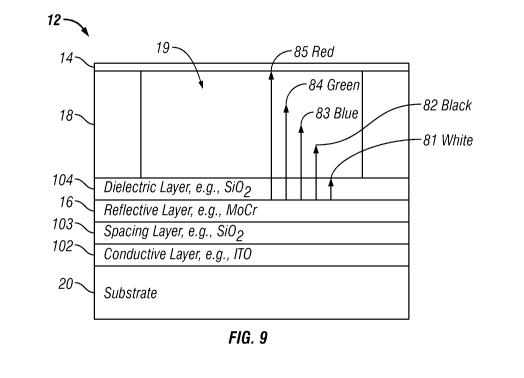
[0075] Figure 9 is a side cross-sectional view of an exemplary multi-state
interferometric modulator 12 with a spacing layer 103. In the multi-state
interferometric
modulator 12, a spacing layer 103 of a material such as silicon dioxide (Si02)
is positioned
between the fixed reflector 16 and the conductive layer 102. The spacing layer
103 increases
the distance between the movable reflector 14 and the conductive layer 102 and
therefore
decreases the capacitance between the movable reflector 14 and the conductive
layer 102 and
provides adequate protection against shorting between the movable reflector 14
and the
conductive layer 102.
[0076] At the same time, the spacing layer 103 defines a second
interferometric
modulating cavity between the fixed reflector 16 and the conductive layer 102.
The thickness
and composition (index of refraction) of the spacing layer 103 can be adjusted
to vary the
effective optical path length of the second interferometric modulating cavity
to produce a
desired color filter. For example, the spacing layer 103 may be adjusted so
that the second
interferometric modulating cavity acts as red, green or blue band pass filters
as desired, and
therefore the multi-state interferometric modulator 12 reflects saturated red,
green or blue
light.
[0077] The reflectance of the conductive layer 102 and the fixed reflector 16
is
low, but the coupled cavity effect exhibited by the first interferometric
modulating cavity and
-19-
CA 02719645 2010-09-24
WO 2009/120610 PCT/US2009/037881
the second interferometric modulating cavities are sufficient to increase the
color saturation
of reflected light.
[0078] Saturation refers to the narrowness of the range of wavelengths of
light
output. A highly saturated hue has a vivid, intense color, while a less
saturated hue appears
more muted and grey. For example, a laser, which produces a very narrow range
of
wavelengths, produces highly saturated light. Conversely, a typical
incandescent light bulb
produces white light that may have a desaturated red or blue color.
[0079] In one embodiment of the display, each pixel includes one or more tri-
state
modulators 12 which have the structure as shown in Figure 9 or similar
structures. These tri-
state modulators include at least a blue modulator, a green modulator, and a
red modulator.
Figure 10 is a schematic side cross-sectional view of a pixel including three
tri-state
interferometric modulators that have respective spacing layers. In Figure 10,
like parts are
numbered similarly with respect to previous figures.
[0080] The blue modulator has three states. In the first state, the movable
reflector 14 is at a first position, for example, position 81, and the blue
modulator
substantially reflects white light. In the second state, the movable reflector
14 is at a second
position, for example, position 82, and the blue modulator substantially
reflects no light. In
the third state, the movable reflector 14 is at a third position, for example,
position 83, and
the blue modulator substantially reflects blue light.
[0081] The green modulator has three states. In the first state, the movable
reflector 14 is at a first position, for example, position 81, and the green
modulator
substantially reflects white light. In the second state, the movable reflector
14 is at a second
position, for example, position 82, and the green modulator substantially
reflects no light. In
the third state, the movable reflector 14 is at a third position, for example,
position 84, and
the green modulator substantially reflects green light.
[0082] The red modulator has three states. In the first state, the movable
reflector
14 is at a first position, for example, position 81, and the red modulator
substantially reflects
white light. In the second state, the movable reflector 14 is at a second
position, for example,
position 82, and the red modulator substantially reflects no light. In the
third state, the
-20-
CA 02719645 2010-09-24
WO 2009/120610 PCT/US2009/037881
movable reflector 14 is at a third position, for example, position 85, and the
red modulator
substantially reflects red light.
[0083] In such an embodiment, light from the red, green, and/or blue
modulators
12 in their third states combines to output colored light. Light from the red,
green, and/or
blue modulators 12 in their first and second states can be used to output
white or black light.
Use of white in combination with color may increase the brightness or
intensity of the pixels.
[0084] In order to increase the saturation of the light from the red, green
and blue
modulators, the thickness and index of refraction of the spacing layer 103 is
selected
respectively for the red, green and blue modulators such that the second
interferometric
modulating cavities in the red, green and blue modulators have corresponding
desired optical
path lengths.
[0085] As described above, the spacing layer 103 can be of any material and of
any thickness. For example, if the spacing layer 103 is of material Si02, the
thickness of the
spacing layer 103 for the red modulator is at least 140 nm. In one embodiment,
when the
thickness of the spacing layer 103 for the red modulator is 170 nm, the red
light from the red
modulator is highly saturated.
[0086] In one embodiment, if the spacing layer 103 is of material Si02, the
thickness of the spacing layer 103 for the blue modulator is at least 210 nm.
When the
thickness of the spacing layer 103 for the blue modulator is 230 nm, the blue
light from the
blue modulator is highly saturated.
[0087] In one embodiment, if the spacing layer 103 is of material Si02, the
thickness of the spacing layer 103 for the green modulator is at least 190 nm.
When the
thickness of the spacing layer 103 for the green modulator is 220 nm, the
green light from the
green modulator is highly saturated.
[0088] The production of an interferometric modulator device incorporating a
spacing layer 103 between the conductive layer 102 and the fix reflector 16
requires only a
few additional process steps compared to the production of an interferometric
modulator
device without the spacing layer 103. In the example illustrated in Figure 9,
incorporation of
the spacing layer 103 requires only an additional step of depositing the
spacing layer 103.
The additional processing requirements can be further reduced or minimized if
the spacing
-21-
CA 02719645 2010-09-24
WO 2009/120610 PCT/US2009/037881
layer 103 comprises the same material as the dielectric layer 104 and/or if
the conductive
layer 102 is made of the same material as the fixed reflector 16.
[0089] Figure 11 shows an example of the modeled reflectance spectra for two
red tri-state modulators. Line 111 depicts the modeled spectral reflectance of
a red tri-state
modulator 12 having a 100 nm thick spacing layer 103 of Si02. Line 112 depicts
the
modeled spectral reflectance of another red tri-state modulator 12 having a
170 nm thick
spacing layer 103 of Si02, to contrast with line 111. As illustrated in Figure
11, the red tri-
state modulator 12 having a 170 nm thick spacing layer 103 of Si02 provides
higher
saturation over the red frequencies, i.e., between 625 nm to 740 nm, than the
red tri-state
modulator 12 having a 100 nm thick spacing layer 103 of SiO2.
[0090] Figure 12 shows an example of combined modeled reflectance spectra for
red, green and blue tri-state modulators having different spacing layers. Line
121 depicts the
modeled spectral reflectance of the blue tri-state modulator 12 having a 230
nm thick spacing
layer 103 of Si02. Line 122 depicts the modeled spectral reflectance of the
green tri-state
modulator 12 having a 220 nm thick spacing layer 103 of Si02. Line 123 depicts
the
modeled spectral reflectance of the red tri-state modulator 12 having a 170 nm
thick spacing
layer 103 of Si02. Line 124 depicts the modeled spectral reflectance when the
red, green and
blue tri-state modulators 12 are in the white state. Line 125 depicts the
modeled spectral
reflectance when the red, green and blue tri-state modulators 12 are in the
black state.
[0091] Figure 13 shows the positions of the red, green, blue, and white colors
perceived in Figure 12 in the CIE 1976 diagram. The color blue which is the
perceived color
of line 121 in Figure 12 is depicted as point 131 in Figure 13. The color
green which is the
perceived color of line 122 in Figure 12 is depicted as point 132 in Figure
13. The color red
which is the perceived color of line 123 in Figure 12 is depicted as point 133
in Figure 13.
The color white which is the perceived color of line 124 in Figure 12 is
depicted as point 134
in Figure 13. As shown in Figure 13, the points 131, 132 and 133 are very
close to the sRGB
primary coordinates, and the point 134 is very close to D65. Here, sRGB is a
standard RGB
color space created cooperatively by HPTM and MicrosoftTM for use on monitors,
printers, and
the Internet. D65 is a standard white point of daylight, which is promulgated
by the
-22-
CA 02719645 2010-09-24
WO 2009/120610 PCT/US2009/037881
International Commission on Illumination (CIE) at the temperature of 6,500 K.
D65
corresponds roughly to a midday sun in Western/Northern Europe.
[0092] Figure 14 shows an example of combined reflectance spectra for a
display
of a three-bit design. In this embodiment, the display has a plurality of red,
green and blue
tri-state modulators. Each pixel comprises a red subpixel, a green subpixel,
and a blue
subpixel. Each of the red, green and blue subpixels is represented by three
bits. For each
subpixel, one tri-state interferometric modulator is associated with the first
bit. Two tri-state
interferometric modulators are associated with the second bit. Four tri-state
interferometric
modulators are associated with the third bit. Therefore, seven tri-state
interferometric
modulators are associated with each subpixel, and twenty one tri-state
interferometric
modulators are associated with each pixel. This embodiment is only an example.
Those
skilled in the art may appreciate that numerous variations are possible.
[0093] Line 141 depicts the spectral reflectance of the blue tri-state
modulators
for the blue subpixel. Line 142 depicts the spectral reflectance of the green
tri-state
modulators for the green subpixel. Line 143 depicts the spectral reflectance
of the red tri-
state modulators for the red subpixel. Line 144 depicts the spectral
reflectance when the red,
green and blue tri-state modulators are in the white state. Line 145 depicts
the spectral
reflectance when the red, green and blue tri-state modulators are in the black
state.
[0094] Experiment with the three-bit design display showed the effects as
shown
in the following table.
Color White Black Red Green Blue
Gamut 38.344
Contrast Ratio 18.359
Brightness (Y) 0.334 0.01819 0.06882 0.1083 0.02269
[0095] As shown above, the three-bit design display demonstrated a modeled
gamut of 38% EBU (European Broadcast Union). The contract ration (CR) was
modeled to
be 18:1. The brightness (Y) was modeled to be 33%.
[0096] Figure 15 shows the positions of the red, green and blue colors
perceived
in Figure 14 in the CIE 1976 diagram. The color blue which is the perceived
color of line
141 in Figure 14 is depicted as point 151 in Figure 15. The color green which
is the
-23-
CA 02719645 2010-09-24
WO 2009/120610 PCT/US2009/037881
perceived color of line 142 in Figure 14 is depicted as point 152 in Figure
15. The color red
which is the perceived color of line 143 in Figure 14 is depicted as point 153
in Figure 15.
The color white which is the perceived color of line 144 in Figure 14 is
depicted as point 154
in Figure 15. As shown in Figure 15, the points 151, 152 and 153 are very
close to the sRGB
primary coordinates, and the point 154 is very close to D65.
[00971 As described above, in a tri-state interferometric modulator, a spacing
layer may be provided between the fixed reflector and the electrodes. The
spacing layer may
provide adequate protection against shorting between the movable device and
the electrodes.
The spacing layer may also define a second interferometric modulating cavity
so as to
provide saturated light over a range of light frequencies. Thus, a display
adopting such tri-
state interferometric modulators may have a longer service life, a higher
contrast ratio and a
larger gamut.
[00981 Although this invention has been disclosed in the context of certain
embodiments and examples, it will be understood by those skilled in the art
that the present
invention extends beyond the specifically disclosed embodiments to other
alternative
embodiments and/or uses of the invention and obvious modifications and
equivalents thereof.
In addition, while several variations of the invention have been shown and
described in
detail, other modifications, which are within the scope of this invention,
will be readily
apparent to those of skill in the art based upon this disclosure. It is also
contemplated that
various combinations or sub-combinations of the specific features and aspects
of the
embodiments may be made and still fall within the scope of the invention. It
should be
understood that various features and aspects of the disclosed embodiments can
be combined
with, or substituted for, one another in order to form varying modes of the
disclosed
invention. Thus, it is intended that the scope of the present invention herein
disclosed should
not be limited by the particular disclosed embodiments described above, but
should be
determined only by the claims that follow.
-24-