Note: Descriptions are shown in the official language in which they were submitted.
CA 02719800 2010-09-27
WO 2009/121041 PCT/US2009/038699
PAPER-BASED MICROFLUIDIC SYSTEMS
CROSS-REFERENCE TO RELATED APPLICATIONS
[0001] This application claims the benefit of U.S. Provisional Application No.
61/039,858, filed March 27, 2008, and U.S. Provisional Application No.
61/039,958,
filed March 27, 2008, the contents of which are hereby incorporated in their
entirety
herein.
BACKGROUND OF THE INVENTION
[0002] Most current bioanalytical assays are inaccessible for developing
economies. Current diagnostic assays typically require large and expensive
laboratory instruments that are operated by trained personnel. Thus, there
remains a
need for low-cost diagnostic assays that are not cumbersome and that can be
performed on small sample volumes. Further, there remains a need for low-cost
systems to detect trace levels of analytes in fluids for, e.g., (i) human
health; (ii)
illicit drug use; (iii) military and homeland security settings; and (iv)
chemical
pollution in the environment.
SUMMARY OF THE INVENTION
[0003] In one aspect, the invention features an assay device. The assay device
comprises a porous, hydrophilic substrate; a fluid-impermeable barrier
defining a
boundary of an assay region and a boundary of a main channel region, the main
channel region fluidically connected to the assay region; and a strip of
conductive
material disposed on the porous, hydrophilic substrate. In some embodiments,
the
porous, hydrophilic substrate comprises nitrocellulose acetate, cellulose
acetate,
cellulosic paper, filter paper, tissue paper, writing paper, paper towel,
cloth, or
porous polymer film.
[0004] In some embodiments, the fluid-impermeable barrier permeates the
thickness of the porous, hydrophilic substrate.
[0005] In some embodiments, the strip of conductive material is disposed on
one
face of the substrate. In some embodiments, the strip conductive material is
disposed on both faces of the substrate. In particular embodiments, the strip
is
positioned to span across the main channel region.
-1-
CA 02719800 2010-09-27
WO 2009/121041 PCT/US2009/038699
[0006] In some embodiments, the conductive material is a metal or a conductive
polymer. In some embodiments, the conductive material is a metal. In
particular
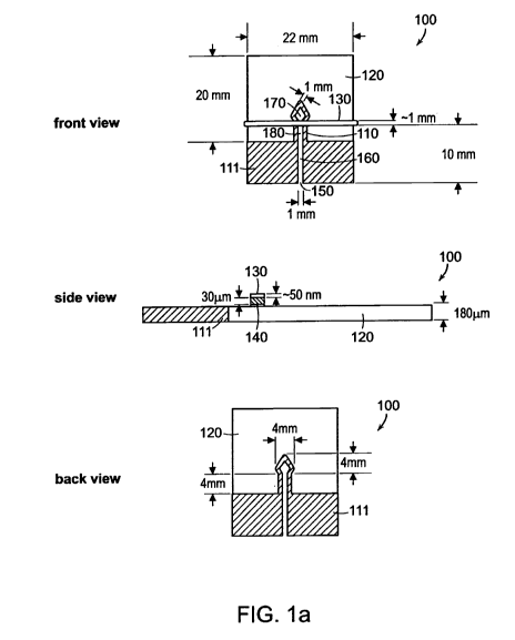
embodiments, the metal is Sn, Zn, Au, Ag, Ni, Pt, Pd, Al, In, or Cu.
[0007] In some embodiments, the assay device further comprises an insulating
material disposed between the conductive material and the porous, hydrophilic
substrate. In some embodiments, the insulating material is tape, polysterene,
polyethylene, or polyvinylchloride.
[0008] In particular embodiments, the main channel region comprises a sample
deposition region, the main channel region providing a fluidic pathway within
the
porous, hydrophilic substrate between the sample deposition region and the
assay
region.
[0009] In some embodiments, the barrier further defines a plurality of assay
regions and a plurality of main channel regions, the strip of conductive
material
spanning two or more channels.
[0010] In yet other embodiments, the assay region comprises a detection
reagent. In some embodiments, the detection reagent is covalently bonded to
the
porous, hydrophilic substrate in the assay region. In other embodiments, the
detection reagent is not covalently bonded to the porous, hydrophilic
substrate in the
assay region.
[0011] In some embodiments, the barrier comprises photoresist or a curable
polymer. In particular embodiments, the barrier comprises SU-8 photoresist.
[0012] In some embodiments, the barrier has at least one dimension between
about 100 m and about 5 cm, between about 100 m and about 1 cm, between
about 100 m and about 1 mm, or between about 100 m and about 200 m. In
some embodiments, the main channel region has at least one lateral dimension
between about 100 m and about 5 cm, between about 100 m and about 1 cm,
between about 100 m and about 1 mm, or between about 100 m and about 200
m. In some embodiments, the layer of conductive material has at least one
lateral
dimension between about 100 m and about 5 cm, between about 100 m and about
1 cm, between about 100 m and about 1 mm, or between about 100 m and about
200 m.
-2-
CA 02719800 2010-09-27
WO 2009/121041 PCT/US2009/038699
[0013] In some embodiments, the conductive material has a resistance of about
S to about 500 Q, about 20 S to about 100 Q, or about 20 S to about 50 Q.
[0014] In another aspect, the invention features an assay device. The assay
device comprises a porous, hydrophilic substrate; a fluid-impermeable barrier
defining (i) a boundary of a main channel region, (ii) boundaries of a first
minor
channel region and a second minor channel region, and (iii) boundaries of a
first
assay region and a second assay region, the first and second minor channel
regions
providing a fluidic pathway within the porous, hydrophilic substrate between
the
main channel region and a corresponding assay region; and a strip of
conductive
material disposed on the porous, hydrophilic substrate. In some embodiments,
the
porous, hydrophilic substrate comprises nitrocellulose acetate, cellulose
acetate,
cellulosic paper, filter paper, tissue paper, writing paper, paper towel,
cloth, or
porous polymer film.
[0015] In some embodiments, the fluid-impermeable barrier permeates the
thickness of the porous, hydrophilic substrate
[0016] In some embodiments, the strip of conductive material is disposed on
one
face of the substrate. In some embodiments, the strip of conductive material
is
disposed on both faces of the substrate.
[0017] In some embodiments, the assay device comprises a second strip of
conductive material. In some embodiments, the second strip of conductive
material
is disposed on both faces of the substrate. In some embodiments, the first and
second strips of conductive material are disposed on the same face or faces of
the
substrate. In some embodiments, the first and second strips of conductive
material
are disposed on opposite faces of the substrate.
[0018] In particular embodiments, the second strip of conductive material is
positioned to span across the second minor channel region. In some
embodiments,
the first strip of conductive material does not span the second minor channel
region.
In some embodiments, the second strip of conductive material does not span the
first
minor channel region.
[0019] In other embodiments, the assay device comprises one or more additional
minor channel regions and one or more additional assay regions, each minor
channel
-3-
CA 02719800 2010-09-27
WO 2009/121041 PCT/US2009/038699
region providing a fluidic pathway between the main channel region and a
corresponding assay region.
[0020] In some embodiments, the conductive material is a metal or a conductive
polymer. In some embodiments, the conductive material is a metal. In
particular
embodiments, the metal is Sn, Zn, Au, Ag, Ni, Pt, Pd, Al, In, or Cu.
[0021] In some embodiments, the assay device further comprises an insulating
material disposed between the conductive material and the porous, hydrophilic
substrate. In some embodiments, the insulating material is tape, polysterene,
polyethylene, or polyvinylchloride.
[0022] In particular embodiments, the main channel region comprises a sample
deposition region, the main channel region providing a fluidic pathway within
the
porous, hydrophilic substrate between the sample deposition region and the
first
minor channel region and the second minor channel region.
[0023] In yet other embodiments, the assay regions comprise a detection
reagent. In some embodiments, the detection reagent is covalently bonded to
the
porous, hydrophilic substrate in the assay region. In other embodiments, the
detection reagent is not covalently bonded to the porous, hydrophilic
substrate in the
assay region.
[0024] In some embodiments, the barrier comprises photoresist or a curable
polymer. In particular embodiments, the barrier comprises SU-8 photoresist.
[0025] In some embodiments, the barrier has at least one dimension between
about 100 m and about 5 cm, between about 100 m and about 1 cm, between
about 100 m and about 1 mm, or between about 100 m and about 200 m. In
some embodiments, the main channel region has at least one lateral dimension
between about 100 m and about 5 cm, between about 100 m and about 1 cm,
between about 100 m and about 1 mm, or between about 100 m and about 200
m. In some embodiments, the layer of conductive material has at least one
lateral
dimension between about 100 m and about 5 cm, between about 100 m and about
1 cm, between about 100 m and about 1 mm, or between about 100 m and about
200 m.
[0026] In some embodiments, the conductive material has a resistance of about
S to about 500 Q, about 20 S to about 100 Q, or about 20 S to about 50 Q.
-4-
CA 02719800 2010-09-27
WO 2009/121041 PCT/US2009/038699
[0027] In another aspect, the invention features a method of controlling the
movement of a fluid sample through an assay device, e.g., an assay device
described
herein. The method comprises applying an electric current to the conductive
material on the assay device; and contacting the main channel region with a
fluid
sample, wherein applying the electric current to the conductive material
prevents the
fluidic flow of the sample from the main channel region to the assay region.
In
some embodiments, applying the electric current evaporates at least a portion
of the
fluid sample and concentrates an analyte at the boundary of the main channel
and
the portion of the conductive material disposed across the main channel
region.
[0028] In some embodiments, the method further comprises removing the
electric current. In particular embodiments, removing the electric current
allows the
fluidic flow of the sample from the main channel to the assay region.
[0029] In another aspect, the invention features a method of controlling the
movement of a fluid sample through an assay device, e.g., an assay device
described
herein and comprising at least two strips of conductive material, each
spanning a
first and second minor channel region, respectively. The method comprises
applying an electric current to a first strip of conductive material; and
contacting the
main channel region with a fluid sample, wherein applying the electric current
to the
first strip of conductive material prevents the fluidic flow of the sample
from a first
minor channel region to a first assay region.
[0030] In some embodiments, applying the electric current evaporates at least
a
portion of the fluid sample and concentrates an analyte at the boundary of the
first
minor channel and the first strip of conductive material.
[0031] In other embodiments, the method further comprises applying an electric
charge to a second strip of conductive material, wherein applying the electric
current
to the second strip of conductive material prevents the fluidic flow of the
sample
from a second minor channel region to a second assay region.
[0032] In some embodiments, the electric current to the strips of conductive
material is turned on or off, allowing or impeding the flow of the fluid
sample
through the corresponding minor channel regions and into corresponding assay
regions.
-5-
CA 02719800 2010-09-27
WO 2009/121041 PCT/US2009/038699
[0033] In another aspect, the invention features a microfluidic device. The
microfluidic device comprises a porous, hydrophilic substrate; a fluid-
impermeable
barrier, the barrier permeating the thickness of the porous, hydrophilic
substrate and
defining within the porous, hydrophilic substrate a boundary of an open-ended
channel having first and second lateral walls; and an electrically conductive
pathway
disposed on the porous, hydrophilic substrate, the electrically conductive
pathway
comprising (i) a strip of conductive material forming an open circuit in the
absence
of an electrically conductive material bridging the first and second lateral
walls; and
(ii) a battery, an electrically-responsive indicator, and a resistor
electrically
connected to the strip of conductive material.
[0034] In another aspect, the invention features a method of detecting the
presence of high electrolyte concentration in a fluid sample. The method
comprises
providing the microfluidic device described herein; and contacting the open-
ended
channel with a fluid sample, wherein the fluid sample flows through the
channel and
bridges the two lateral walls of the channel, completing the electrically
conductive
pathway, wherein a detectable signal produced by the electrically-responsive
indicator upon the completion of the electrically conductive pathway is
indicative of
a high electrolyte concentration in the fluid.
BRIEF DESCRIPTION OF THE DRAWINGS
[0035] The foregoing and other objects of the present invention, the various
features thereof, as well as the invention itself, may be more fully
understood from
the following description, when read together with the accompanying drawings,
in
which:
[0036] FIG. IA is a schematic illustration of a paper-based microfluidic
system
having a single detection zone. FIG. lB is a schematic illustration of a paper-
based
microfluidic system having four detection zones.
[0037] FIG. 2 is a schematic illustrating a method for fabricating prototype -
PAD devices for concentrating analytes in fluids.
[0038] FIG. 3A is a representation of a photograph of a -PAD connected to a
tunable current source. FIG. 3B is a schematic of a -PAD depicting locations
on
the device where temperature was measured using an IR thermometer. FIG. 3C is
a
-6-
CA 02719800 2010-09-27
WO 2009/121041 PCT/US2009/038699
series of representations of photographs depicting a time course of a heated -
PAD
dipped into 165 M allura red AC. FIG. 3D is a series of representations of
photographs of identical -PAD devices. FIG. 3E is a graph of the relative
percent
increase in color in the triangular tips of heated devices over time.
[0039] FIG. 4 is a schematic diagram of a paper-based microfluidic device and
its use to measure dehydration.
[0040] FIG. 5 is a schematic diagram of a method of fabricating a paper-based
microfluidic device to measure dehydration.
[0041] FIG. 6A is a graph of the electrical resistance of a microfluidic
channel
vs. the concentration of NaCl in the solution that fills the channel. Inset
shows a
representation of a photograph of the device used for the experiments. FIG. 6B
is a
graph of the electrical resistance of a microfluidic channel vs. time for a
100 mM
solution of NaCl in water.
[0042] FIG. 7 is a schematic drawing of the device.
[0043] FIG. 8 is a series of representations of photographs of microfluidic
devices. FIG. 8A depicts a device that has the right switch turned on and the
left
switch turned off. FIG. 8B depicts a device that has the right switch turned
on and
the left switch turned off. FIG. 8C and FIG. 8D depict one device; with either
the
right switch on (FIG. 8C), or the right switch off (FIG. 8D).
[0044] FIG. 9 is a series of representations of photographs of a multiple-
channel
microfluidic device with a wire crossing 8 of 16 channels. FIG. 9A depicts
sequential images of the flow and control of solution of blue dye using curved
wire.
FIG. 9B depicts an enlargement of one channel with wire. FIG. 9C depicts the
same
device subsequently used to control the flow of yellow dye. FIG. 9D depicts an
enlargement of one channel with wire.
[0045] FIG. 10 is a series of representations of photographs of a multiple-
channel microfluidic device with switches. FIG. 1 OA depicts the set of
channels
with an applied wave-shape wire across the device. FIG. I OB depicts an
enlargement of channel nr 8 from FIG. 10A.
[0046] FIG. 11 is a schematic of a 3-D programmable microfluidic device.
-7-
CA 02719800 2010-09-27
WO 2009/121041 PCT/US2009/038699
DETAILED DESCRIPTION
[0047] All publications, patent applications, patents, and other references
mentioned herein are incorporated by reference in their entirety. In addition,
the
materials, methods, and examples are illustrative only and not intended to be
limiting. Unless otherwise defined, all technical and scientific terms used
herein
have the same meaning as commonly understood by one of ordinary skill in the
art
to which this invention belongs. Although methods and materials similar or
equivalent to those described herein can be used in the practice or testing of
the
present invention, suitable methods and materials are described below.
General
[0048] Under some aspects, porous, hydrophilic substrates are patterned with
hydrophobic barriers to provide a class of low-cost, portable, and technically
simple
platforms for running multiplexed bioassays on biological liquids. One example
of
a useful hydrophilic substrate for assays is paper, which is inexpensive,
readily
commercially available, disposable, wicks liquids quickly, and does not need
careful
handling as do some conventional platforms. The paper or other porous,
hydrophilic
substrate is patterned with hydrophobic barriers that provide spatial control
of
biological fluids and enable fluid transport due to capillary action within
the regions
the barriers define. The hydrophobic barriers can be polymeric, for example a
curable polymer or a photoresist, and provide a substantially impermeable
barrier
throughout the thickness of the porous, hydrophilic substrate within defined
areas.
[0049] The paper or other porous, hydrophilic substrate also includes a layer
of
conductive material, e.g., metal, affixed to one side of the substrate. The
conductive
material can be used to control the flow of a fluid sample through the
substrate, e.g.,
to concentrate analytes in fluids and for detecting trace levels of multiple
analytes in
a sample, or to create "switches" and "valves" to control the flow of fluid
samples
into different regions of a bioassay. The switches and valves are compatible
with
two-dimensional (2-D), lateral-flow paper-based microfluidic devices as well
as
three-dimensional (3-D), flow-through devices (which consist of alternating
layers
of paper and tape stacked on top of one another). The combination of switches
and
valves leads to simple, inexpensive, and paper-based microfluidic devices that
-8-
CA 02719800 2010-09-27
WO 2009/121041 PCT/US2009/038699
control the movement of fluids precisely without the added complication of
pumps
or other external equipment for function.
[0050] In some embodiments, an insulating material layer is disposed between a
conductive material and a porous, hydrophilic substrate. Non-limiting examples
of
insulating material that can be used include tape, polysterene, polyethylene,
polyvinylchloride, thin film photoresist, polyimide, glues, epoxies, wax,
PDMS,
silicone, latex, or any other suitable insulating polymers, or any combination
thereof.
In some embodiments, a conductive material is attached to an insulating
material
layer to form a composite sheet (e.g., an insulated conductive layer).
Assay Devices
[0051] Fig. IA is a schematic illustration of an assay device having a
hydrophilic substrate, hydrophobic barriers, and conductive materials
according to
some embodiments of the invention. The device 100 includes a patterned
hydrophobic barrier 110, e.g., SU-8 photoresist, porous, hydrophilic substrate
120,
e.g., chromatography paper, a conductive material 130, e.g., metal, and
insulating
layer 140, e.g., tape. The hydrophobic barrier 110 defines regions in the
substrate
120 that can be used to perform bioassays. In the illustrated embodiment,
barrier
110 defines a sample deposition region 150, where a fluid sample can be
deposited,
assay region 170, and main channel region 160, which wicks the fluid sample by
capillary action from deposition region 150 to assay region 170.
[0052] When electric current is applied to conductive material 130, the
conductive material 130 becomes warm and this heat is transferred through
insulating layer 140 and into main channel region 160. Since the conducting
material 130 and insulating layer 140 are placed on one side of device 110,
the fluid
in main channel region 160 can evaporate from the back side of device 110.
Thus,
when electric current is applied to conductive material 130, the fluid sample
wicks
through main channel region 160 to region 180, where conductive material 130
contacts hydrophobic barrier 110, and does not flow to assay region 170.
[0053] Fig. 3C is a series of images depicting the flow of an aqueous solution
of
allura red AC through the assay device 110 of Fig. IA with and without
electric
current being applied to conductive material. The solution flowed from sample
-9-
CA 02719800 2010-09-27
WO 2009/121041 PCT/US2009/038699
deposition region 150 through main channel region 160 to region 180, at the
region
that conducting material 130 contacts hydrophobic barrier 110. The fluid
sample did
not flow to assay region 170. The amount of dye continued to accumulate at
region
180 for 13 minutes, as the fluid evaporated at region 180. At 13 minutes, the
electric
current to conductive material 130 was turned off. By 13.5 minutes, the fluid
sample began to flow into assay region 170. As described in greater detail
below,
assay region 170 can be treated with a detection reagent to detect the
presence of a
particular analyte within the fluid sample.
[0054] Fig. lB is a schematic illustration of an assay device 100 having
patterned hydrophobic barrier 110, e.g., SU-8 photoresist, porous, hydrophilic
substrate 120, e.g., chromatography paper, a conductive material 130, e.g.,
metal,
and insulating layer 140, e.g., tape. The hydrophobic barrier 110 defines a
sample
deposition region 150, where a fluid sample can be deposited, assay regions
171,
172, 173, 174, minor channel regions 191, 192, 193, 194, and main channel
region
160, which wicks the fluid sample by capillary action from deposition region
150 to
assay regions 171, 172, 173, and 174 through minor channel regions 191, 192,
193,
and 194, respectively. When electric current is applied to conductive material
130,
the fluid sample wicks through main channel region 160 to region 180, where
conductive material 130 contacts hydrophobic barrier 110, and does not flow to
minor channel regions 191, 192, 193, or 194. Assays regions 171, 172, 173, and
174
can be treated with detection reagents, e.g., the same or different detection
reagents,
to detect the presence of particular analytes within the fluid sample.
[0055] In device 100 depicted in Fig. 1B, assay regions 171, 172, 173, and 174
are spaced equally from main channel region 160 (about 2 mm from main channel
region 160). In this embodiment, assay regions 171, 172, 173, and 174 receive
equal
volumes of fluid sample, and assay regions 171, 172, 173, and 174 fill at a
similar
rate.
[0056] In the devices illustrated in Fig. IA and 1B, main channel region 160
is 1
mm wide. In other embodiments, main channel region 160 is narrower, e.g.,
around
100 m, to accommodate for small fluid sample volumes (e.g., less than about 3
L). The devices in Fig. IA and Fig. lB also include a region 111 of paper
-10-
CA 02719800 2010-09-27
WO 2009/121041 PCT/US2009/038699
embedded with SU-8 photoresist, which can prevent fluids from entering the
device
adventitiously.
[0057] Fig. 7 is a schematic illustration of an assay device having a
hydrophilic
substrate, a hydrophobic barrier, and two layers of conductive materials. The
device
200 includes a patterned hydrophobic barrier 210, e.g., SU-8 photoresist,
porous,
hydrophilic substrate 220, e.g., chromatography paper, conductive material
layers
231 and 232, and insulating layers 241 and 242. The hydrophobic barrier 210
defines a sample deposition region 250, where a fluid sample can be deposited,
assay regions 271 and 272, minor channel regions 291 and 292, and main channel
region 260, which wicks the fluid sample by capillary action from deposition
region
250 to assay regions 271 and 272 through minor channel regions 291 and 292,
respectively. Assays regions 271 and 272 can be treated with detection
reagents,
e.g., the same or different detection reagents, to detect the presence of
particular
analytes within the fluid sample.
[0058] When electric current is applied to conductive material layer 231,
conductive material layer 231 becomes warm and this heat is transferred
through
insulating layer 241 and into minor channel region 291. Since the conducting
material layer 231 and insulating layer 241 are placed on one side of device
210, the
fluid in minor channel region 291 can evaporate from the back side of device
210.
Thus, when electric current is applied to conductive material layer 231, the
fluid
sample wicks through main channel region 260 to minor channel region 291 to
region 281, where conductive material layer 231 contacts hydrophobic barrier
110,
and does not flow to assay region 271. When electric current is applied to
conductive material layer 231, the fluid sample flows from main channel region
250
to assay region 272 through minor channel region 292.
[0059] When conductive material layers 231 and 232 are about 60-70 C, the
movement of fluid is stopped (is switched off), and when the temperature of
conductive material layers 231 and 232 is below 60 C, the movement of fluid
is
modulated (creating valves). The time required to turn on and off the switches
and
valves (i.e., the time for conductive material layers 231 and 232 to heat and
cool) is
less than 1 s at 0.2 volts, but can be adjusted by applying different levels
of current.
Both components can be turned on and off many times.
-11-
CA 02719800 2010-09-27
WO 2009/121041 PCT/US2009/038699
[0060] Figs. 8A and 8B are images depicting the flow of an aqueous solution of
red dye through the assay device 210 of Fig. 7. Conductive material layers 231
and
232 were 1 mm-wide x 50 nm-thick gold conductive pathways deposited onto one
side of insulating layers 241 and 242 (30 m-thick). As depicted in Fig. 8A,
when
electric current was applied to conductive material layer 232, the fluid
sample
flowed from main channel region 260 to assay region 271. However, the fluid
sample did not flow to assay region 272, but was stopped at region 282. As
shown
in Fig. 8B, when the electric current to conductive material layer 232 was
turned off
and an electric current was applied to conductive material layer 231, the
fluid
sample flowed from main channel region 260 to assay region 272 and stopped
flowing to assay region 271, accumulating at region 281.
[0061] Fig. 11 is a schematic illustration of a device 300 that includes a
seven-
segment liquid display, which can be used to display all numbers from 0 to 9.
Device 300 includes patterned hydrophobic barrier 310, porous, hydrophilic
substrate 320, and conductive material layers 330. The hydrophobic barrier 310
defines display regions 370, minor channel regions 390, and main channel
region
360, which wicks fluid by capillary action to display regions 370 through
minor
channel regions 390. When electric current is applied to conductive material
layer
330, the fluid sample wicks through main channel region 360 to region 380,
where
conductive material layer 330 contacts hydrophobic barrier 310, and does not
flow
into display regions 370. By turning current on and off to conductive material
layers
330, fluid movement into display regions 370 can be controlled to display a
particular number 0 to 9.
[0062] These devices present many advantages. For example, the devices use
only a heating element (e.g., a flat, 30- m-thin wire) to control the flow of
the liquid
in the channel. There are no mechanical valves or stoppers to control the flow
of the
fluid in the channel. The device has simple, thin and flat heating wires that
"act" as
a valve/switch. These valves/switches can direct the liquid very precisely and
can
"hold" (stop) the liquid in one position for hours (more than 2 h). With this
method,
the rate, direction and path of the flow can be controlled. This device is
lightweight
and thin, and can be bent or flexed. Paper is hydrophilic and chemically
inert, can
convey the liquid without external pumps due to the capillary forces. Paper
-12-
CA 02719800 2010-09-27
WO 2009/121041 PCT/US2009/038699
channels are biocompatible. Paper can be chemically modified or functionalized
to
immobilize for example, capturing agents. Further, the fabrication process is
inexpensive and can be done within an hour.
Microfluidic Devices for Measuring Electrolyte Concentrations in Fluid Samples
[0063] In one aspect, a microfluidic device for measuring salt concentrations
in
fluidic samples is described. The microfluidic device contains a patterned
hydrophilic substrate with patterned hydrophilic regions, electrically
conductive
material pathways deposited onto the hydrophilic substrate, electronic
components
attached to the electrically conductive material pathways, and a microfluidic
channel
for depositing a fluid sample within one of the hydrophilic regions. The
patterned
hydrophilic substrate contains a fluid-impermeable barrier which substantially
permeates the thickness of the hydrophilic substrate and defines boundaries of
one
or more hydrophilic regions within the hydrophilic substrate, as described
herein.
[0064] A variety of electrical components can be attached to the electrically
conductive material pathways. Non-limiting examples of electronic components
include integrated circuits, resistors, capacitors, transistors, diodes,
mechanical
switches, batteries, and external power sources. Non-limiting examples of
batteries
include button cell (watch) battery. Non-limiting examples of external power
source
include an AC voltage source. The electrical components can be attached using,
e.g., known adhesives. In certain embodiments, a commercially available two-
part
conductive adhesive (Circuit Specialists Inc.) is prepared by mixing equal
volumes
of the components in a Petri dish. This adhesive can be used immediately after
mixing and is applied to the conductive material pathways using a syringe
needle.
Discrete electronic components are bonded to the metallic pathways by pressing
the
terminals of the electronic component on the adhesive.
[0065] The microfluidic channel for depositing a fluid sample can be any of
the
hydrophilic regions that is in contact with the conductive material pathways.
The
microfluidic channel for depositing a fluid sample, the conductive material
pathways, and the electronic components are fabricated in such a way that when
a
fluid sample is introduced to the microfluidic channel, it came into contact
with the
conductive material pathways to complete a circuit containing the fluid, the
- 13 -
CA 02719800 2010-09-27
WO 2009/121041 PCT/US2009/038699
conductive material pathways, and the electric components. In one or more
embodiments, a fluid sample containing salt is introduced to the microfluidic
channel. The concentration of salt within the fluid sample determines the
resistance
of the fluid sample, which in turn determines the electrical current of the
circuit. In
certain embodiments, a light-emitting diode (LED) is attached to the
conductive
material pathways. In certain specific embodiments, a fluid sample with high
salt
concentration and low resistance is introduced to the microfluidic channel and
are in
contact with the conductive material pathways. An electrical current passes
through
the circuit, a sufficient voltage is built across the LED, and the LED is
turned on. In
certain other specific embodiments, a fluid sample with low salt concentration
and
high resistance is introduced to the microfluidic channel and are in contact
with the
conductive material pathways. An insufficient voltage is built across the LED,
and
the LED remains on.
[0066] In other embodiments, a portion of the microfluidic channel for
depositing a fluid sample is sealed from air to limit evaporation of the fluid
sample
during use after the assembly of the device. The portion sealed can be 50%,
60%,
70%, 80% 90%, or 95% of the microfluidic channels. In certain embodiments, the
portion of the microfluidic channel is sealed by applying scotch tape to
either side of
the device. In certain other embodiments, the section of the microfluidic
channel for
depositing the fluid sample is not sealed. In certain specific embodiments,
the
section of the microfluidic channel adjacent to the edge of the patterned
hydrophilic
substrate is not sealed so that it could serve as the entrance to the
microfluidic
channel for depositing the fluid sample.
[0067] In one specific embodiment, a microfluidic device 20 made out of
patterned paper for measuring salt concentrations in fluidic samples is
described
with reference to Figure 4. As shown in Figure 4A, microfluidic device 20
contain
patterned paper 1, metallic pathways 5, 11, 12, 13, electric components 4 and
7, and
a microfluidic channel 8. Paper 1 is patterned by photoresist 2 using any of
the
methods described in W02008/049083, the contents of which are hereby
incorporated by reference. Metallic pathways 5, 11, 12, 13 are deposited onto
paper
substrate 1. A resistor 4 (100 kf2) to modulate the current is attached to
metallic
pathways 5 and 11. A button cell (watch) battery 6 to supply the electrical
current is
-14-
CA 02719800 2010-09-27
WO 2009/121041 PCT/US2009/038699
attached to metallic pathways 5 and 13. A light-emitting diode (LED) 7 is
attached
to metallic pathways 12 and 13. A microfluidic channel 8 defined by part of
photoresist 2 resides between metallic pathways 11 and 12 so that when a fluid
sample is introduced into the microfluidic channel 8, a circuit is completed
consisting the fluid sample, metallic pathway 11, resistor 4, metallic pathway
5,
button cell battery 6, metallic pathway 13, LED 7, and metallic pathway 12. A
plastic tape 3 is used to seal a portion of the microfluidic device as shown
in Figure
4A with edge 14 of the microfluidic channel 8 left unsealed. As shown in
Figure
4B, a fluid sample 9 is introduced to the edge 14 of the microfluidic channel
8. The
fluid sample is wicked to fill the microfluidic channel 8 so that metallic
pathways 11
and 12 are now electrically connected as shown in Figure 4C. When the fluid
sample 9 has low resistance, an electrical current 10 passes through the
circuit, a
sufficient voltage is built across LED 7, and LED 7 is turned on. In this
embodiment, microfluidic channel 8 is 1 mm wide and the fluid sample 9 can be
a
urine or sweat sample with a volume of 50-100 L supplied by a patient.
[0068] Patients suffering from dehydration have bodily fluids (e.g., sweat and
urine) with higher concentration of NaCl than patients who are adequately
hydrated.
These concentrated salt solutions, in turn, have a lower electrical resistance
than
fluids with low salt concentration. Dehydration can be measured using the
device
described in this embodiment by passing an electrical current through the
metallic
pathways and the fluid sample 9 in the microfluidic channel 8. The device 20
measures the resistance of the fluid sample 9, and therefore, the level of
dehydration
in the patient. When fluid of high salt content (e.g., indicative of
dehydration) fills
the channel, the resistance of the circuit contributed by the fluid sample 9
is low,
allowing sufficient voltage to build across (bias) LED 7, turning it on. This
can
indicate that a patient may be dehydrated. When fluid of low salt content
(e.g.,
indicative of adequate hydration) fills the channel 8, the resistance of the
circuit
contributed by the fluid sample 9 is high, preventing sufficient voltage to
build
across the LED 7 and the LED 7 remains off, indicating that the patient is
likely
adequately hydrated. The resistor 4 is used to limit the current of the
circuit, and to
match the threshold voltage bias necessary to illuminate the LED 7 with the
- 15 -
CA 02719800 2010-09-27
WO 2009/121041 PCT/US2009/038699
minimum concentration of salt in a biological sample, e.g., urine or sweat,
e.g.,
indicative of dehydration.
[0069] The microfluidic device described functions without any external
equipment and is lightweight and portable (the flat profile of the device
makes it
easy to stack and to store in binders, folders or other inexpensive and
ubiquitous
carrying cases already available for paper. The microfluidic device described
are
disposable and, therefore, more resistant to contamination than reused assays.
The
microfluidic device described are biodegradable and can be disposed of safely
by
incineration. The microfluidic device described requires only very small
volumes of
the sample fluid. In certain embodiments, only about 15 L of urine, sweat, or
other
bodily fluids is required for analysis. In addition, the microfluidic device
described
can enable quick diagnoses. In certain embodiments, dehydration in patients
can be
diagnosed in less than 10 s from the time of applying a droplet of urine or
sweat to
the microfluidic device.
Porous, Hydrophilic Substrates
[0070] Any porous, hydrophilic substrate that wicks fluids by capillary action
can be used as the substrate in the methods and devices described herein.
Nonlimiting examples include cellulose and cellulose acetate, paper (e.g.,
filter
paper and chromatography paper), cloth, and porous polymer film.
[0071] Preferably, the porous, hydrophobic substrate is paper. Paper can be
patterned easily into regions of hydrophilic paper demarcated by walls of
hydrophobic polymer; is hydrophilic and wicks fluids by capillary action, so
no
external pump is needed to move fluids within the microfluidic channels; is
available with a variety of pore sizes that are useful for filtering solid
contaminants
and particulates from a fluid; is thin and lightweight; is very inexpensive
and is
available throughout the world; can be incinerated easily for disposal of
hazardous
waste after an assay; and can be modified covalently to alter the chemistry
(and
function) of an assay device.
Methods of Patterning
[0072] Exemplary methods for patterning hydrophobic barriers are described in
W02008/049083. For example, some embodiments of the assay devices are made
-16-
CA 02719800 2010-09-27
WO 2009/121041 PCT/US2009/038699
using photolithography by saturating the porous, hydrophilic substrate with
photoresist, exposing the saturated substrate to a pre-determined pattern of
light, and
removing the photoresist based on the pattern, forming hydrophobic barriers
made
of photoresist. The pattern of the light can be selected to define assay
regions,
channel regions, sample deposition regions, and the like, the boundaries of
which are
at least partially defined by the hydrophobic barriers. Such methods provide a
significantly high feature resolution. For example, these photolithographic
techniques can be used to make barriers having a thickness between about 1 mm
and
about 100 m, e.g., between about 300 m and 100 m, or even smaller.
Additionally, the techniques can form features that do not vary significantly
along
their length, e.g., barriers having widths that vary by less than about 10%,
by less
than about 5%, or even less, along their length. Conversely, channels defined
by
such barriers will also have widths that do not vary significantly along their
length,
e.g., by less than about 10%, by less than about 5%, or even less, along their
length.
Methods of Depositing Electrically Conductive Materials
[0073] In one aspect, microfluidic devices which incorporate electrically
conductive materials onto hydrophilic substrates is described. Deposition of
electrically conductive materials onto hydrophilic substrates of the
microfluidic
devices using a variety of methods is described.
[0074] Hydrophilic substrates can be any substrate that wicks fluids by
capillary
action. Non-limiting examples of hydrophilic substrates include
nitrocellulose,
cellulose acetate, paper, cloth, and porous polymer film. Non-limiting
examples of
paper include filter paper and chromatographic paper.
[0075] Non-limiting examples of electrically conductive materials include
metal,
conductive polymers, conductive grease, conductive adhesives, any other
material
that is electrically conductive, or a combination thereof. In one or more
embodiments, the conductive materials include metal. Non-limiting examples of
metals include Sn, Zn, Au, Ag, Ni, Pt, Pd, Al, In, Cu, or a combination
thereof. In
other embodiments, the conductive materials include conductive polymers. Non-
limiting examples of conductive polymers include polyacetylenes, polypyrroles,
polyanilines, poly(thiophene)s, poly(fluorene)s, poly(3-alkylthiophene)s,
-17-
CA 02719800 2010-09-27
WO 2009/121041 PCT/US2009/038699
polytetrathiafulvalenes, polynaphthalenes, poly(p-phenylene sulfide),
poly(para-
phenylene vinylene)s, or any combination or derivative thereof. In yet other
embodiments, the conductive materials include conductive grease, conductive
adhesives or any other material that is electrically conductive.
[0076] A variety of deposition methods could be used to deposit electrically
conductive materials onto the hydrophilic substrates of the microfluidic
devices.
Non-limiting examples of the deposition methods include depositing conductive
materials using stencils, depositing conductive materials by drawing
conductive
pathways, depositing conductive materials by inkjet or laser printing,
depositing
conductive materials by attaching commercially available or homemade
conductive
material tapes onto the hydrophilic substrates, depositing conductive
materials by
drawing conductive pathways, or depositing conductive materials by introducing
conductive fluids onto the hydrophilic substrates or the hydrophilic channels
of the
microfluidic devices. Alternatively, conductive materials could be embedded in
the
pulp or fibers for manufacturing the hydrophilic substrates to allow for
manufacturing hydrophilic substrates containing conductive materials.
[0077] In one or more embodiments, the conductive materials are deposited onto
the hydrophilic substrates of the microfluidic devices using stencils by a
variety of
techniques.
[0078] Stencils contain a pattern of holes or apertures through which
conductive
materials could be deposited onto the hydrophilic substrates. Alternatively,
in a
etching process, stencils contain a pattern of holes or apertures through
which
conductive materials could be etched to form a pattern of metal on the
hydrophilic
substrates. Stencils could be made from a variety of materials such as metal,
plastic,
or patterned layers of dry-film resist. Non-limiting examples of metals for
manufacturing stencils include stainless steel and aluminum. Non-limiting
examples
of plastic for manufacturing stencils include mylar. Alternatively, patterned
layers
of dry-film resist can be used as stencils. In one or more embodiment, metals
or
plastics are used to manufacture stencils and patterns of metallic pathways
can be
designed on a computer using a layout editor, (e.g., Clewin, WieWeb Inc.) and
stencils based on the design can be obtained from any supplier (e.g., Stencils
Unlimited LLC (Lake Oswego, OR)). In certain embodiments, the stencil can be
-18-
CA 02719800 2010-09-27
WO 2009/121041 PCT/US2009/038699
removed from the paper after deposition. In certain other embodiments, one
side of
the stencil is sprayed with a layer of spray-adhesive (e.g., 3M Photomount, 3M
Inc.)
to temporarily affix the stencil to the paper substrate. After deposition, the
stencil
can be peeled away from the paper. The stencils can be reused multiple times,
e.g.,
more than 10 times. In other embodiments, patterned layers of dry-film resist
can be
used as stencils. Dry film resist can be patterned when exposed to UV light
through
a transparency mask and developed in dilute sodium hydroxide solution. The
patterned dry-film resist can be attached to a coating sheet of plastic or
directly
affixed to the hydrophilic substrates by pressing the resist-side to the
surface of the
hydrophilic substrates and passing multi-sheet structure through heated
rollers in a
portable laminator (Micro-Mark, Inc). The coating sheet of plastic can then be
peeled away, resulting in a sheet of paper with dry film resist patterned on
one side.
[0079] A variety of techniques could be used to deposit electrically
conductive
materials onto the hydrophilic substrates of the microfluidic devices through
stencils. Non-limiting examples of such techniques include evaporating through
stencils, sputter-depositing through stencils, spray-depositing through
stencils,
squeegeeing through stencils, or evaporating or sputter-depositing a thin
layer of
conductive material through stencils followed by developing a thicker layer of
conductive material by electrodeposition or electroless deposition.
Alternatively, a
conductive material is first deposited onto a hydrophilic substrate by
evaporation,
sputter-deposition, spray-deposition, or squeegee. A stencil is then applied
and the
part of the conductive material that is not protected by the stencil is etched
to form a
pattern of conductive material on the hydrophilic substrates.
[0080] In one or more embodiments, conductive materials are evaporated onto
the hydrophilic substrates of the microfluidic devices through stencils.
Evaporation
is a method of thin film deposition in which the source material is evaporated
in a
vacuum. The vacuum allows vapor particles to travel directly to the target
object
(substrate), where they condense back into a solid state. Detailed
descriptions of
evaporation deposition can be found in S. A. Campbell, Science and Engineering
of
Microelectronic Fabrication, Oxford University Press, New York (1996), which
is
hereby incorporated by reference in its entirety. Evaporating requires a high
vacuum, is applicable to a variety of metals, and can deposit metal at rates
of up to
-19-
CA 02719800 2010-09-27
WO 2009/121041 PCT/US2009/038699
50 nm/s. In certain embodiments, conductive materials such as metals are
evaporated onto the hydrophilic substrates through stencils made of metal,
plastic, or
photoresist. In certain other embodiments, conductive materials are evaporated
onto
the hydrophilic substrates through stencils made of metal or plastic based on
a silk-
screen soaked in photoresist. In yet certain other embodiments, a thin layer
of
conductive materials is evaporated onto the hydrophilic substrates and then
the a
thicker layer of conductive materials is deposited by electrodeposition or
electroless
deposition. In certain specific embodiments, metal is evaporated on paper
using an
e-beam evaporator. Non-limiting examples of metal in these embodiments include
100% Sn, 100% In, 100% Au, 100% Ag, 52%In-48%Sn Eutectic, 100% Ni and
100% Zn.
[0081] In other embodiments, conductive materials are sputter-deposited onto
the hydrophilic substrates of the microfluidic devices through stencils.
Sputter
deposition is a physical vapor deposition method of depositing thin films by
sputtering, i.e., ejecting, material from a source onto a substrate, e.g., a
hydrophilic
substrate. Detailed descriptions of sputtering deposition can be found in S.
A.
Campbell, Science and Engineering of Microelectronic Fabrication, Oxford
University Press, New York (1996). Sputter-deposition is usually performed at
a
lower vacuum (>75,000 Torr) and deposits conductive materials such as metals
at a
lower rate than evaporation (e.g., 1 nm/s for Au, with lower rates and higher
energy
requirements for other metals). In certain embodiments, conductive materials
such
as metals are sputter-deposited onto the hydrophilic substrates through
stencils made
of metal, plastic, or photoresist. In certain other embodiments, conductive
materials
are sputter-deposited onto the hydrophilic substrates through stencils made of
metal
or plastic based on a silk-screen soaked in photoresist. In yet certain other
embodiments, a thin layer of conductive materials is sputter-deposited onto
the
hydrophilic substrates and then the a thicker layer of conductive materials is
deposited by electrodeposition or electroless deposition. In certain specific
embodiments, metal is deposited onto paper by sputtering using a Cressington
208HR benchtop sputter coater. Non-limiting examples of metal in these
embodiments include 100% Pt, 100% Au, 80% Pd / 20% Pt, 100% Ag, 100% Ni,
100% Al and 100% Sn. In another specific embodiment, Au (gold) is sputtered
onto
-20-
CA 02719800 2010-09-27
WO 2009/121041 PCT/US2009/038699
a hydrophilic substrate. Gold has an electrical conductivity similar to that
of copper
or aluminum (electrical conductivity = 45.17 x 10⁶ 1/em, at 20 C). Gold wires
with a small cross sectional area (50 nm x 1 mm) over several centimeters long
can
form conductive metallic pathways with high resistance (>100 S2). Such gold
wires
can be heated to high temperatures (about 90 C) using modest voltages (about
5 V)
and currents (about 55 mA), which can be supplied easily by portable alkaline
or Li-
ion batteries. Alternatively, a section of tape can be affixed directly onto
the
hydrophilic substrates and then gold is sputter-deposited through a mask onto
the
tape.
[0082] In yet other embodiments, conductive materials are spray-deposited onto
the hydrophilic substrates of the microfluidic devices through stencils. Spray-
deposition is quick and inexpensive and can be applied at room temperature
without
specialized equipment. Also, because of its large coating thickness, spray
deposition
of metal can be used to build electrically conductive pathways on very rough
surfaces including toilet paper, paper towel, or even woven fabric. The spray
is
applied via an airbrush or an aerosol container consisting of flakes of
conductive
materials such as metals suspended in an acrylic base. In certain embodiments,
conductive materials such as metals are spray-deposited onto the hydrophilic
substrates through stencils made of metal, plastic, or photoresist. In certain
other
embodiments, conductive materials are spray-deposited onto the hydrophilic
substrates through stencils made of metal or plastic based on a silk-screen
soaked in
photoresist. In certain specific embodiments, Ni or Ag is sprayed onto a
substrate
and curing at room temp (10 min) produces an electrically conductive surface
(thickness = 20-100 gm depending on number of passes, surface resistance = 0.7
Q/square for Ni, 0.01 Q/square for Ag).
[0083] In yet other embodiments, conductive materials are squeegeed onto the
hydrophilic substrates of the microfluidic devices through stencils. Non-
limiting
examples of electrically conductive materials that can by squeegeed onto the
hydrophilic substrates include solder paste, conductive grease, conductive
adhesive
or conductive ink (metal or conductive polymer based). Squeegee techniques can
be used to deposit conductive materials on the surface or into the inside of
the
hydrophilic substrates. In certain embodiments, conductive materials such as
metals
-21-
CA 02719800 2010-09-27
WO 2009/121041 PCT/US2009/038699
are squeegeed onto the hydrophilic substrates through stencils made of metal,
plastic, or photoresist. In certain other embodiments, conductive materials
are
squeegeed onto the hydrophilic substrates through stencils made of metal or
plastic
based on a silk-screen soaked in photoresist.
[0084] In yet other embodiments, conductive materials are deposited onto the
hydrophilic substrates of the microfluidic devices using a etching process
through
stencils. In certain embodiments the conductive material is first deposited
onto the
hydrophilic material by evaporation, sputter-deposition, spray-deposition, or
squeegee. A stencil is then applied and the part of the conductive material
deposited
onto the hydrophilic substrates that is not protected by the stencil is
etched, resulting
in a pattern of the electrically conductive material on the hydrophilic
substrate. In
certain specific embodiments, conductive materials such as metals are
deposited
onto the hydrophilic substrates and then through stencils, the deposited
metals are
subjected to a reactive-ion etching process to remove the part of the metal
deposit
which is not protected by the stencil, resulting a pattern of metal on the
hydrophilic
substrates.
[0085] In yet other embodiments, conductive materials are deposited by drawing
conductive pathways on hydrophilic substrates. In certain embodiments, metals
are
deposited onto the hydrophilic substrates using pens filled with conductive
metal
inks. Non-limiting examples of metal in these embodiments include Ag and Ni.
In
certain other embodiments, conductive polymers are deposited onto the
hydrophilic
substrates using pens filled with conductive polymers. Drawing conductive
pathways could deposit conductive materials both on the surface and inside the
matrix of the hydrophilic substrates.
[0086] In yet other embodiments, conductive materials are deposited by inkjet
or
laser printing. In certain embodiments, conductive polymers are printed or
plotted
by inkjet or laser printing. In certain other embodiments, a conductive ink is
printed
or plotted by inkjet or laser printing.
[0087] In yet other embodiments, conductive materials are deposited by
attaching commercially available or homemade conductive material tapes onto
the
hydrophilic substrates. In certain embodiments, commercially-available
conductive
tape is affixed onto the surface of the hydrophilic substrates. Non-limiting
examples
-22-
CA 02719800 2010-09-27
WO 2009/121041 PCT/US2009/038699
of commercially-available conductive tapes include copper tape. In certain
other
embodiments, homemade conductive tape is affixed onto the surface of the
hydrophilic substrates. Non-limiting examples of homemade conductive tapes
include plastic tape such as scotch tape coated with conductive materials by
evaporation, sputter-deposition, spray-deposition or squeegee.
[0088] In yet other embodiments, conductive materials are deposited by
introducing conductive fluids onto the hydrophilic substrates or the
hydrophilic
channels of the microfluidic devices. In certain embodiments, conductive
fluids are
wicked into the hydrophilic substrates or the hydrophilic channels. Non-
limiting
examples of conductive liquids include ionic solutions, metals, carbon-
nanotube
solutions, or conductive polymers.
[0089] In yet other embodiments, conductive materials could be embedded in
the pulp or fibers for manufacturing the hydrophilic substrates to allow for
manufacturing hydrophilic substrates with conductive materials deposited
within. In
certain embodiments, metals or other conductive materials are embedded in the
pulp
or fibers used for manufacturing paper.
[0090] In another aspect, electrical components are attached onto the
hydrophilic
substrates after the deposition of conductive materials. The electrical
components
can be attached using, e.g., known adhesives. In certain embodiments, a
commercially available two-part conductive adhesive (Circuit Specialists Inc.)
can
be prepared by mixing equal volumes of the components in a Petri dish. This
adhesive can be used immediately after mixing and is applied to the conductive
material pathway using a syringe needle. Discrete electronic components are
bonded to the metallic pathways by pressing the terminals of the electronic
component on the adhesive. Non-limiting examples of electronic components
include integrated circuits, resistors, capacitors, transistors, diodes,
mechanical
switches, and batteries.
[0091] Fig. 2 schematically illustrates a method for depositing conductive
materials to make an assay device described herein. As shown in Fig. 2, an
insulating layer 1 (30 m thick) is first attached to a porous, hydrophilic
substrate 2
(30 m thick). A conductive metal layer 3 (50 nm thick) is then deposited onto
the
insulating layer 1 by sputter deposition. The formed sandwich of conductive
metal-
-23-
CA 02719800 2010-09-27
WO 2009/121041 PCT/US2009/038699
insulating layer-porous, hydrophobic substrate layers is then cut into
sections and
within one of the sections, the insulating layer 1 (with the conductive metal
layer 3
attached) is detached from porous, hydrophilic substrate 2 to form a
conductive
metal-insulating layer assembly 11 containing 12, a section of the conductive
metal
layer, and 13, a section of the insulating layer. The conductive metal-
insulating
layer assembly 11 is then attached to a patterned porous, hydrophilic
substrate 5
with hydrophobic material 4 permeating the thickness of selected portions of
the
patterned porous, hydrophilic substrate 5. The formed sandwich of conductive
metal-insulating layer-porous, hydrophilic substrate layers can be cut into
sections
with a variety of shapes and sizes and the insulating layers within the
sections (with
the conductive metal layer attached) can be detached from the porous,
hydrophilic
substrate to form conductive metal-insulating layer assemblies with different
shapes
and sizes.
Detection Reagents
[0092] The bounded regions of the hydrophilic substrate can be used to define
one or more assay regions in an assay device. The assay regions of the
bioassay
device can be treated with reagents that respond to the presence of analytes
in a
biological fluid and that can serve as an indicator of the presence of an
analyte. In
some embodiments, the response to the analyte is visible to the naked eye. For
example, the hydrophilic substrate can be treated in the assay region to
provide a
color indicator of the presence of the analyte. Indicators may include
molecules that
become colored in the presence of the analyte, change color in the presence of
the
analyte, or emit fluorescence, phosphorescence, or luminescence in the
presence of
the analyte. In other embodiments, radiological, magnetic, optical, and/or
electrical
measurements can be used to determine the presence of proteins, antibodies, or
other
analytes.
[0093] In some embodiments, to detect a specific protein, an assay region of
the
hydrophilic substrate can be derivatized with reagents, such as small
molecules, that
selectively bind to or interact with the protein. Or, for example, to detect a
specific
antibody, an assay region of the hydrophilic substrate can be derivatized with
reagents such as antigens, that selectively bind to or interact with that
antibody. For
-24-
CA 02719800 2010-09-27
WO 2009/121041 PCT/US2009/038699
example, reagents such as small molecules and/or proteins can be covalently
linked
to the hydrophilic substrate using similar chemistry to that used to
immobilize
molecules on beads or glass slides, or using chemistry used for linking
molecules to
carbohydrates. In alternative embodiments, the reagents may be applied and/or
immobilized by applying them from solution, and allowing the solvent to
evaporate.
The reagents can be immobilized by physical absorption onto the porous
substrate
by other non-covalent interactions. In general, a wide variety of reagents can
be
used with the assay devices to detect analytes, and can be applied by a
variety of
suitable methods. These reagents could include antibodies, nucleic acids,
aptamers,
molecularly-imprinted polymers, chemical receptors, proteins, peptides,
inorganic
compounds, and organic small molecules. These reagents could be adsorbed to
paper (non-covalently through non-specific interactions), or covalently (as
either
esters, amides, imines, ethers, or through carbon-carbon, carbon-nitrogen,
carbon-
oxygen, or oxygen-nitrogen bonds).
[0094] However, the interaction of some analytes with some reagents may not
result in a visible color change, unless the analyte was previously labeled.
The
device can be additionally treated to add a stain or a labeled protein,
antibody,
nucleic acid, or other reagent that binds to the target analyte after it binds
to the
reagent in the assay region, and produces a visible color change. This can be
done,
for example, by providing the device with a separate area that already
contains the
stain, or labeled reagent, and includes a mechanism by which the stain or
labeled
reagent can be easily introduced to the target analyte after it binds to the
reagent in
the assay region. Or, for example, the device can be provided with a separate
channel that can be used to flow the stain or labeled reagent from a different
region
of the paper into the target analyte after it binds to the reagent in the
assay region. In
one embodiment, this flow is initiated with a drop of water, or some other
fluid. In
another embodiment, the reagent and labeled reagent are applied at the same
location in the device, e.g., in the assay region.
Biological Samples
[0095] The microfluidic systems described herein can be used for assaying
sample fluids. Biological samples that can be assayed using the diagnostic
systems
-25-
CA 02719800 2010-09-27
WO 2009/121041 PCT/US2009/038699
described herein include, e.g., urine, whole blood, blood plasma, blood serum,
cerebrospinal fluid, ascites, tears, sweat, saliva, excrement, gingival
cervicular fluid,
or tissue extract.
[0096] In some embodiments, a single drop of liquid, e.g., a drop of blood
from
a pinpricked finger, is sufficient to perform assays providing a simple yes/no
answer
to the presence of an analyte, or a semi-quantitative measurement of the
amount of
analyte that is present in the sample, e.g., by performing a visual or digital
comparison of the intensity of the assay to a calibrated color chart. However,
in
order to obtain a quantitative measurement of an analyte in the liquid, a
defined
volume of fluid is typically deposited in the device. Thus, in some
embodiments, a
defined volume of fluid (or a volume that is sufficiently close to the defined
volume
to provide a reasonably accurate readout) can be obtained by patterning the
paper to
include a sample well that accepts a defined volume of fluid. For example, in
the
case of a whole blood sample, the subject's finger could be pinpricked, and
then
pressed against the sample well until the well was full, thus providing a
satisfactory
approximation of the defined volume.
Applications
[0097] The microfluidic systems to measure salt concentrations in solutions
described herein can be used in a number of different applications. For
example,
they can be useful for pediatric physicians (for diagnosis of dehydration in
infants or
other patients in which it is difficult to obtain large volumes of urine);
physicians
working in resource-poor settings such as developing countries (for diagnosing
dehydration in environments where the cost of the assays or the availability
of
electricity for running instruments are of primary concern); physicians
working in
emergency or point-of-care environments (as a method for detecting dehydration
rapidly); nurses or caregivers in nursing homes (for testing dehydration in
the
elderly); military technologists (for monitoring dehydration in soldiers);
athletes,
trainers, or sports physicians/technicians (for testing dehydration in
athletes "on-the-
field" in practice or in competition); veterinarians (for testing dehydration
in
domestic pets, livestock, racehorses, or other animals.); farmers or
agricultural
scientists/engineers (for testing dehydration in plants and animals);
environmental
-26-
CA 02719800 2010-09-27
WO 2009/121041 PCT/US2009/038699
scientists (for testing the concentration of salt in water); and chemists,
bioengineers,
or chemical engineers (as a blueprint for building other disposable electronic-
microfluidic hybrid devices in paper substrates).
[0098] The microfluidic systems incorporating switches and valves described
herein can be used in many applications. For example, they can be adapted to
perform reactions in channels (e.g., PCR, nucleic acid synthesis). Further,
paper
devices with heating elements can be used by chemists for conducting
(bio)chemical
reaction within such system (e.g., as a lab-on-a-chip device). In some
embodiments,
the product can be directly synthesized in the reacting chamber, purified by
chromatography (simply by migration to other channels), and separated from the
chip by cutting a piece of paper.
[0099] In other embodiments, the devices incorporating switches and valves can
be used as a model system in understanding the flow of the liquid, heat
transfer and
its influence on the stream in porous media (see Figures 10 and 11). The
devices
can also be a used to investigate the presence of small molecules in versatile
fluids
(e.g., blood, urines, saliva, and water) by concentrating them directly before
adding
a fresh reagent. The switches can enable one to perform the reaction next to a
control analyte or to compare how the concentration influences the detection
(e.g.,
while one switch is on and the analyte in the fluid is concentrating, the
other channel
is filled with non-concentrated analyte, and at the end analytes in both
channels can
be reacted with the reagent). These devices can also be used in microfluidic
experiments when the number of different liquids or reagents that can be added
to
the system, either in doses or simultaneously, is limited.
[0100] The use of metals in paper as microfluidic devices can also be adapted
and used in any of the following applications: pumping fluids in paper;
concentrating analytes in paper by evaporation; "switching" fluids in paper or
controlling the directional flow of fluids, or turning on/off the flow of
fluids in
paper; performing electrochemical reactions in paper (e.g., redox); paper-
based
batteries or fuel cells; sensing temperature of fluids in paper; heating
fluids in paper
(e.g., for reactions or incubation of cells); PCR in paper; cooling fluids in
paper
(e.g., when metal is used as a conductor of "cold" from a cooling device such
as a
Peltier cooler); concentrating magnetic fields in paper microfluidic devices
(e.g.,
-27-
CA 02719800 2010-09-27
WO 2009/121041 PCT/US2009/038699
nickel pattern + external permanent magnet); applying magnetic fields in paper
for
separations, trapping, or capturing particles or analytes; applying electrical
or
magnetic fields in paper for mixing (e.g., using small particles that shake
around);
electrophoresis in paper microfluidic channels; capacitive detection in paper
(e.g.,
sense difference in dielectric); sensing the ionic resistance in paper (e.g.,
for
detecting salt content); sensing the electrical resistance in paper (e.g., a
paper
diagnostic device where silver reduction in a microfluidic channel produces a
conductive pathway of given resistance proportional to the analyte being
detected);
complex electrically-actuated fuses (e.g., where the microfluidic channels
contain an
explosive, e.g., gasoline); self-destructive paper diagnostics (e.g., where
the fuse is
actuated by the electronics eliminating the need for an external spark or
flame); and
portable, remote-sensing diagnostic devices (e.g., diagnostics that take
measurements and then send signals long distances via RF communication).
[0101] The invention is further illustrated by the following examples. The
examples are provided for illustrative purposes only. They are not to be
construed
as limiting the scope or content of the invention in any way.
EXAMPLE S
Example 1 - Preparation and Use of Paper Microfluidic Device for Analyte
Concentration
Fabricating a paper micro fluidic device
[0102] The prototype -PADs was fabricated in a two step process (see Figure
2). The -PADs were prepared in a two-step process that involved creating
patterns
of hydrophobic polymer in paper, and patterning conductive gold pathways onto
the
paper-based microfluidic devices.
[0103] First, the microfluidic channels were formed in Whatman filter paper 1
using photolithography and SU-8 photoresist, as described previously (Martinez
et
al., Angew. Chem. Int. Ed., Eng. 46:1318-1320, 2007). Briefly, this process
involved embedding SU-8 photoresist into Whatman filter paper 1, drying the
paper
to remove the cyclopentanone in the SU-8 formula, and then irradiating the
paper for
around 3.5 min (using a 100 W mercury lamp) through a pattern of black ink
printed
-28-
CA 02719800 2010-09-27
WO 2009/121041 PCT/US2009/038699
onto a transparency. The paper was heated at 90 C for 10 min, soaked in
propylene
glycol methyl ether acetate (3 x 5 min) and methanol (3 x 5 min), and dried.
[0104] The gold conductive pathways were then patterned onto the paper-based
microfluidic device by first preparing the wires, and then affixing them to
the
microfluidic device. For these devices, gold was patterned onto tape and the
tape
was cut into appropriately sized conductive pathways for affixing to the
devices.
Specifically, the wires were fabricated by affixing the sticky side of Scotch
Transparent Tape to unbleached parchment paper, and by sputtering a 50 nm
layer
of gold onto the shinny side of the tape using a Cressington Model 208HR
sputter
coater set to 60 mA and 50 s sputtering time (see Figure 2). The
gold/tape/parchment paper composite was cut into sections sized appropriately
for
the -PAD (i.e., a straight section with dimensions of 30 m x 1 mm x 22 mm
for
the single channel -PAD, and a continuous U-shaped section with dimensions of
30
m x 1 mm x 21 mm at the base of the U, and 30 m x 1 mm x 15 mm on the sides
of the U for the multiple channel -PAD). The parchment paper was peeled from
the gold/tape composite, and the tape was affixed to the paper-based
microfluidic
devices around 0.5 mm below the bottom of the detection zones. This distance
was
far enough from the detection zones to minimize transfer of heat from the wire
to the
reagents deposited in the zones.
Concentrating aqueous red dye
[0105] The effectiveness of the device for concentrating an analyte was tested
by
concentrating an aqueous solution of 165 M allura red AC (a red food
coloring)
using a single channel -PAD fabricated as described above. Alligator clips
(micro
flat alligator clips, Mueller Electric Inc.) were used to connect the gold
wires on
each device to a tunable current source (see Figure 3a). In Figure 3a, the
allura red
AC solution has reached the wire and has become slightly concentrated. Each
metal
wire had a resistance of around 100 Q. Passing current through the device
(around
55 mA) for 5 s heated the metal. The temperature of the wire was measured
using
an IR Thermometer (Figure 3b). The temperature of the paper on the back side
of
the -PAD (i.e., on the opposite side of the wire) was also measured, and an
immediate increase of temperature of the channel from 23 C to around 75 5
C
-29-
CA 02719800 2010-09-27
WO 2009/121041 PCT/US2009/038699
was observed when voltage was applied. There was an approximately 5 C
variation
in the final temperature of the channel that reflected small differences in
width of the
gold wires.
[0106] Initially, the device was suspended above a 5 mL aqueous solution of
allura red AC (165 M). The aqueous solution then was raised until it
contacted the
bottom of the paper (with the current turned on). The aqueous solution wicked
into
the central channel of the device and reached the wire in 30-60 s. As the
solution
wet the hydrophilic channel adjacent to the wire, the temperature of the
channel
decreased by around 3-5 C (at 23% relative humidity). The fluid did not
continue
wicking up the central channel beyond the wire when the channel was warmed
above 60 C. Instead, the heat from the wire was absorbed by the solution,
leading
to evaporation of the water in proximity to the wire.
[0107] When the fluid evaporated, the allura red AC was concentrated in the
portion of the channel aligned with the wire (Figure 3c). The fluid continued
to
evaporate and the analyte became increasingly concentrated as long as current
was
passed through the [t-PAD. The channel underneath the wire was heated to -70
C.
Current (55 mA) was applied continuously for 13 min and then reduced to zero.
After turning off the current, the channel cooled within seconds and the fluid
wicked
into the remaining portions of the device. In the orientation depicted in
Figure 3c,
the gold wire was on the back of the devices. The location of the wire is
highlighted
by dotted lines in the photograph of the device after 1 min of heating. The
concentrated allura red AC appeared as the dark material below the detection
zone.
In this example, the device was heated for a maximum of 13 min, but the device
can
be heated and the analyte concentrated until the fluid is consumed.
[0108] When the current was turned off, the channel cooled from 65-75 C to 23
C in less than 5 s. As soon as the channel cooled to -40 C, the fluid began
wicking into the remaining portions of the device. The close proximity of the
wire
to the detection zones ensured that the concentrated analyte moved as a plug
with
the liquid and remained concentrated as it filled the diamond-shaped regions
(Figure
3c).
-30-
CA 02719800 2010-09-27
WO 2009/121041 PCT/US2009/038699
Relationship between length of heating and concentration of analyte
[0109] The relationship between the length of time that a sample was heated
and
the relative amount that the analyte was concentrated was measured by wicking
165
M allura red AC in water into multiple -PADS. The devices were heated for
different periods of time and then cooled to allow the fluid to fill the
detection
zones. The relative percent increase in color that collected in the ends of
the devices
was measured by photographing the dry devices and by obtaining the mean
intensity
of color for the terminal triangular region of each device using Adobe
Photoshop .
The triangular regions were scanned using the blue channel in Adobe Photoshop
,
and the relative percent increase in allura red AC was calculated using the
following
equation:
colorno heating - colorheating (n min)
relative % increase = x 100
colorno heating
[0110] The extent to which color developed in the triangular tips of the
devices
depended on the length of time that current was passed through the gold wire
(Figure 3d). In Figure 3d, identical -PAD devices were heated for varying
lengths
of time and then cooled to allow the concentrated samples to wick into the
pentagon-
shaped ends of the devices. The heating time started when the fluid reached
the wire
in the central channel and ended when the current was reduced to zero. When
the
device was heated for short periods of time (1 min), the color was only 10%
higher
than devices run in the absence of applied current (Figure 3e; the data were
fit with a
linear least-squares line described by the following equation: y = 5.92x +
3.81; R2 _
0.96). When heated for 13 min, however, the color was 73% more intense than
devices that were not heated.
Example 2 - Preparation and Use of Paper Microfluidic Device for Detecting
Salt Concentration
Fabricating a paper micro fluidic device
[0111] Microfluidic channels were fabricated in filter paper (Whatman, Inc.)
using a process described previously (Martinez et al., Angew. Chem. Int. Ed.,
Eng.
46:1318-1320,2007) (see Figure 5). The patterns for the microfluidic channels
were
-31-
CA 02719800 2010-09-27
WO 2009/121041 PCT/US2009/038699
designed on a computer using a layout editor (Clewin, WieWin Inc.) and a
photomask was printed from the design using an inkjet printer and a
transparency
film. The microfluidic channels were patterned in Whatman filter paper 1 using
the
following process: (i) paper (2.5 cm x 2.5 cm x 200 m) was soaked in resist
(SU-8
2010, Microchem Inc.), and a rolling pin was used to press excess resist from
the
paper; (ii) the paper was dried for 10 min at 95 C, the photomask was clamped
to
the paper by pressing them together as a sandwich between two glass slides
that
were held together with binder clips, and the paper was exposed to UV light
(100 W
mercury spot lamp) through the photomask to transfer the pattern of the mask
to the
paper; and (iii) the paper was developed by soaking it in propylene glycol
monomethyl ether acetate (2 x 10 min) and propan-2-ol (2 x 10 min).
Fabricating metallic wires on the micro fluidic devices
[0112] Patterns of metallic pathways were designed on a computer using a
layout editor (Clewin, WieWeb Inc.) and a stainless steel stencil was obtained
from
Stencils Unlimited LLC (Lake Oswego, OR) based upon the design.
[0113] The metal was deposited on the paper-based microfluidic device by
manually aligning the stencil to the features patterned in the paper, and by
evaporating conductive metal (100% In) through the stencil. The metal was
patterned on either side of the microfluidic channel and extended over the
edges of
the hydrophobic barrier defining the channel and into the hydrophilic channel,
such
that when fluid filled the microfluidic channel, it came into contact with the
metal to
complete the circuit.
[0114] After depositing the metal, 90% of the microfluidic channel was sealed
from air by applying scotch tape to either side of the device. This step
limits
evaporation of fluid during use. The section of microfluidic channel adjacent
to the
edge of the paper was not sealed so that it could serve as the entrance to the
microfluidic channel for the fluid.
Mounting electronic components to the paper
[0115] The electronic components were attached to the device using a process
described above. A commercially available two-part conductive adhesive
(Circuit
Specialists Inc.) was prepared by mixing equal volumes of the parts in a Petri
dish.
-32-
CA 02719800 2010-09-27
WO 2009/121041 PCT/US2009/038699
Immediately after mixing: (i) the adhesive was applied to the metallic
pathways
using a syringe and needle, and (ii) the electronic components-the resistor,
LED,
and battery- were bonded to the metallic pathways by pressing the terminals of
the
electronic components on the adhesive. The epoxy set in less than 15 min,
forming
permanent electrical connections between the components and the conductive
pathways on the paper. The complete device comprised a 3 V button (watch)
battery
(Energizer Inc., $0.20), a resistor (Digikey Inc., $0.01) and a light-emitting
diode
(Lumex Inc. $0.08) (see Figure 4).
Measuring the electrical resistance of aqueous salt solution in a paper-
based micro fluidic channel
[0116] Six identical microfluidic devices were fabricated as discussed above.
The microfluidic channel in each device was filled with aqueous solutions
containing different concentration of NaCl: 0 mM, 50 mM, 100 MM, 250 mM, 500
mM, and 1000 mM.
[0117] The electrical resistance of the fluid-filled microfluidic channel in
each
device was determined by connecting the metal wires fabricated on either side
of the
channel to a voltage source (BK Precision, Inc.) biased at 1 V, and by
measuring the
electrical current passing through the channel with a digital multimeter
(Fluke, Inc.).
The electrical resistance of the channel was obtained by dividing the bias
voltage by
the current.
[0118] Figure 6a shows the steady-state resistance of the channel as a
function
of the concentration of NaCl in the solution. All values were collected at 60
s, at
which the resistance that was measured was near steady state in all samples.
The
plot shows that the channel exhibited highest resistance when the water in the
channel contained no added salt. As the concentration of salt in the solution
was
increased, the resistance of the channel decreased. Error bars represent the
range of
data across three experiments using three separate, identical devices.
[0119] Figure 6b shows the resistance of the channel as a function of time
after
applying the droplet of solution to the device. At t = 0, the resistance of
the channel
was approximately 5 MQ. Within 10 s, the resistance reduced to an approximate
-33-
CA 02719800 2010-09-27
WO 2009/121041 PCT/US2009/038699
steady-state value of 20 kQ. Error bars represent the range of data across
three
experiments using three separate, identical devices.
Example 3 - Preparation and Use of Paper Microfluidic Device with Switches
and Valves
Fabrication of the devices
[0120] The microfluidic devices were fabricated using a process that consisted
of three general steps: (i) photolithography on a Whatman filter paper 1 using
SU-8
photoresist, according to product specifications (MicroChem Corp., Newton,
MA);
(ii) fabrication and attachment of metal-tape wires: 50 nm layer of gold was
sputtered (Cressington Model 208HR sputter coater, 60 mA, 50 s sputtering
time)
onto a matt side of the Scotch tape and attached to the device as a 1-mm-wide
strip;
and (iii) assembling all the layers of the device.
Switching the channels on/off
[0121] To investigate the switching on/off process in the paper channel, an
aqueous solution of red dye (0.05 mM aq. disodium 6-hydroxy-5-((2-methoxy-5-
methyl-4-sulfophenyl)azo)-2-naphthalene-sulfonate, allura red) was used to
visualize the effectiveness of the device. The solution was conveyed to the
central
channel of the device by capillary action. The heating wire was set to 70 C
to stop
the flow of the liquid.
[0122] The wires were connected with a tunable current source using alligator
clips. The voltage was set to 0.1 V, current 0.037 mA. The device was immersed
in
the aqueous solution of the dye to about 500 m deep into the solution to
introduce
the liquid into the channel by capillary action. To turn off one channel (to
close it),
the current that was passing through the wire across that channel was adjusted
to
give about 80 C (the temperature was measured with IR thermometer), while the
other wire was not turned on (the temperature on that wire was about 30 C)
allowing the liquid to flow (Figure 8).
[0123] When the flow from the central channel was directed to the channel 1,
the current on the switch 2 was turned on and the switch 1 was turned off
(Figure
8A). The temperature on the switch 1 was 30 C. The temperature on the switch
2
-34-
CA 02719800 2010-09-27
WO 2009/121041 PCT/US2009/038699
was 80 C. The cooling time was less than 1 s. The time needed to reach 80 C
was
also less than 1 s. When the switch 2 was turned off, the liquid started to
flow into
that channel (Figure 8B). The liquid was not entering into the channel 1 since
the
current on the wire 1 was turned on. The switches 1 and 2 were periodically
turned
on and off to guide the flow of the liquid. (The liquid was continuously
supplied in
this experiment). After stopping the flow of the liquid in channel 2 (Figure
8C), the
switch 2 was turned off and the liquid could flow further into the channel
(Figure
8D).
Simultaneous control of thee flow of the liquid in multiple channels
[0124] Single metal-tape hybrid wire was attached across the set of multiple
channels in order to stop the liquid at different length of those channels.
The wire
was positioned in the manner so the switch was placed at a different part of
each
channel. In this particular experiment, a conductive pen was used to draw the
wire
(just to simplify the process but the same approach could be conducted using a
metal-tape hybrid wire). The wire was drawn on the transparent tape attached
to the
paper device (Figure 10). To visualize the flow of the liquid, blue or yellow
dye
[0.05 mM aq. erioglaucine (ammonium, ethyl(4-(p-(ethyl(m-sulfobenzyl) amino)-
alpha-(o-sulfophenyl) benzylidene)-2,5- cyclohexadien-1-ylidene) (m-
sulfobenzyl)-
, hydroxide, inner salt, disodium salt) and 0.05 mM aq. tartrazine (4,5-
dihydro-5-
oxo-l-(4-sulophenyl)-4-[(4-sulfophenyl)azo]-1 H-pyrazole-3-carboxylic acid
trisodium salt), respectively] was added to MilliQ water. The colored liquid
was
delivered to the device by immersion of channel(s) into the solution. In a
first
experiment (Figure 10), an aqueous solution of blue dye was introduced to the
channels and the liquid was stopped by the round/curved wire that was crossing
8
out of 16 channels (Figures 1 OA and l0B). The wire was heated up to 70 C in
order
to stop the flow of the liquid. Half of the channels were serving as a
reference to
follow the flow of the liquid without heating. When the heating was off, the
liquid
passed through the channel until it filled it up completely.
[0125] Subsequently another dye (yellow dye) was introduced to the same
device, and the solution was stopped where the wire was attached (Figures I OC
and
-35-
CA 02719800 2010-09-27
WO 2009/121041 PCT/US2009/038699
10D). Multiple components can be injected to the system which can be useful
in, for
example, the synthesis on the chip.
[0126] In a second experiment, a wave-shape wire was drawn across channels
using conductive pen (Figure 1 IA). The wire was heated up to 70 C. The flow
of
the liquid was stopped along various lengths of the channels, in the place
were the
wire was crossing. In places where the wire was very close to the end of the
channel, a high concentration of the dye was observed (Figure 11B) while at
the
position where the wire was far from the end of the channel dilution process
accrued.
EQUIVALENTS
[0127] It is to be understood that while the invention has been described in
conjunction with the detailed description thereof, the foregoing description
is
intended to illustrate and not limit the scope of the invention, which is
defined by the
scope of the appended claims. Other aspects, advantages, and modifications are
within the scope of the following claims.
-36-