Note: Descriptions are shown in the official language in which they were submitted.
CA 02719955 2010-09-29
WO 2009/121186 PCT/CA2009/000434
High-Speed Video Serializer and Deserializer
[00011 The present application claims the benefit of copending U.S. Serial No.
61/042,471
filed April 4, 2008 and entitled High-Speed Video Serializer and Deserializer
the entirety of
which is hereby incorporated by reference for all purposes.
TECHNICAL FIELD
[00021 The technology described in this document relates generally to the
field of digital
audio/video signal processing. More particularly, this document describes a
high-speed video
serializer and deserializer.
BACKGROUND
[00031 At present, if board designers want to transmit or receive 3 Gb/s SDI
to/from a field-
programmable gate array (FPGA), they have two options. First, they may use
high-speed
transceiver I/Os such as those included on Xilinx Virtex 5 FPGAs (Rocket IOs)
or the high-
speed transceivers on Altera's Stratix II GX series of FPGAs. Second, they may
use a 20-bit
parallel interface with clock and data operating at 148.5 MHz. The first
option is problematic
due to the jitter performance of high-speed transceivers, the high cost of
FPGAs with these
transceivers, and the limited number of high-speed transceivers on one FPGA.
The second
option presents the problems: (1) that it uses many I/Os on the FPGA, where in
many cases
FPGA designs run out of I/Os before they run out of logic, so I/Os are at a
premium, and (2)
because the parallel interface has so many traces, it is not suitable for
running across a backplane
or for designing a small daughter card.
[00041 Two commercially available products that address the above problems are
the
National Semiconductor LMH0340 3Gb/s serializer and LMH0341 3Gb/s
deserializer. These
products provide 3-Gb/s serialization and deserialization functions, and
reduce the parallel bus
between the serializer and FPGA from a 20-bit single-ended interface to a 5-
bit low-voltage
differential signaling (LVDS) interface. This simplifies board layout by
reducing the number of
traces between the serializer, deserializer and FPGA. The LVDS signaling
scheme reduces
-1-
CA 02719955 2010-09-29
WO 2009/121186 PCT/CA2009/000434
electromagnetic interference (EMI), while the narrow parallel bus enables a
single low-cost
FPGA to support a greater number of high-speed video channels.
100051 The National Semiconductor products consist of 5 differential LVDS data
lanes and
one differential LVDS clock lane (for a total of 12 required FPGA pins). The
maximum FPGA
pin speed is 600 Mb/s (DDR pixel clock) which is achievable using dedicated
LVDS lanes in the
FPGA. The National deserializer does not do descrambling and word alignment,
so the FPGA
must further demultiplex the 5-bit bus to 10 or 20 bits, and then perform
these operations to
detect timing reference signals. In addition, the National serializer does not
do SMPTE
scrambling, so this operation must be done in the FPGA, along with partial
serialization (20 bits
to 5 bits). In the event there is excess skew on the board between the
deserializer and the FPGA
(> 1 data word), the scrambled data bits may appear out of order at the input
of the deserializer.
When this misaligned data is descrambled, the output will appear to be
corrupted - no video or
timing reference signals (TRS) can be extracted. Therefore, skew must be very
carefully
managed during layout. LVDS I/Os, due to differential design, are inherently
more noise
immune than LVCMOS, and generate less EMI as long as the trace layout is done
carefully on
the board.
SUMMARY
[00061 The improvement described herein is a transmitter/receiver (also known
as an SDI
serializer/deserializer) with the ability to receive/transmit 10-bit parallel
video data with a dual-
data rate (DDR) pixel clock over a single-ended interface. The DDR clock is
used when the SDI
data bandwidth is 3Gb/s. In this case, the 10-bit parallel data rate is
297Mb/s, and the frequency
of the DDR clock is 148.5 MHz. One benefit of the disclosed parallel data
interface is to reduce
the number of pins required to connect the transmitter and receiver devices
with FPGAs in the
video system. Because the parallel bus is single-ended, the total number of
required pins is 11
(10-bits data + 1-bit pixel clock). This is of significance because FPGA
designs are often pin-
limited. In addition, the DDR pixel clock avoids the need to operate a high-
drive pixel clock at
297 MHz, which reduces power consumption, clock drive strength requirement,
and noise
generation. It also enables easier board routing and avoids the need to use
the higher-speed I/Os
on FPGAs, which may require more expensive speed grades. FIG. 1 demonstrates
how the DDR
-2-
CA 02719955 2010-09-29
WO 2009/121186 PCT/CA2009/000434
interface operates. The pixel clock is transmitted at half the data rate, and
the interleaved data is
sampled at the receiver on both clock edges.
[0007] According to one embodiment, a high-speed video serializer is comprised
of an X bit
parallel input bus and a Y bit parallel output bus, where X and Y are
multiples of one another
(e.g., 2). A multiplexer is connected between the input bus and the output bus
and is operated
such that a frequency of the signals on the output bus is a multiple of the
frequency of the signals
on the input bus. A circuit provides a clock signal substantially in sync with
the signals on the
output bus.
[0008] According to another embodiment, a high-speed video deserializer is
comprised of an
X bit parallel input bus responsive to received data signals, and a Y bit
parallel output bus. The
X and Y buses are multiples of one another (e.g., 2). A circuit receives and
provides a sampling
clock signal substantially in sync with the signals on the input bus. A
splitter circuit is
responsive to the input bus and a first data sampling circuit is responsive to
the splitter circuit for
detecting data on a positive edge of the sampling clock. A second data
sampling circuit is
responsive to the splitter circuit for detecting data on a negative edge of
the sampling clock. The
Y bit parallel output bus is responsive to the first and second data sampling
circuits.
[0009] Methods of operating the disclosed serializer and deserializer are also
disclosed.
BRIEF DESCRIPTION OF THE FIGURES
[0010] For the disclosed improvement to be easily understood and readily
practiced, the
disclosed improvement will now be described, for purpose of illustration and
not limitation, in
conjunction with the following figures.
[0011] FIG. 1 illustrates how the disclosed dual data rate interface operates.
[0012] FIG. 2 is a block diagram of one embodiment of a dual data rate
serializer according
to the present disclosure.
[0013] FIG. 3 is a block diagram of one embodiment of a dual data rate
deserializer
according to the present disclosure.
[0014] FIGs. 4A and 4B are block diagrams illustrating two potential locations
for the
disclosed serializer.
-3-
CA 02719955 2010-09-29
WO 2009/121186 PCT/CA2009/000434
DETAILED DESCRIPTION
[0015] The disclosed improvement reduces the parallel FPGA interface to only
11 pins: 10
single-ended data lanes plus one single-ended DDR clock lane. The maximum
operating data
rate with a 148.5 MHz DDR clock is 297Mbps, which is achievable in low-cost
FPGAs.
Because the receiver will also perform SMPTE descrambling as well as word
alignment (to
detect timing reference signals), the FPGA can process the data immediately,
without further
deserialization or word alignment. In addition, because the transmitter
performs SMPTE
scrambling, the FPGA can output 10-bit data without having to do the
scrambling step. Both the
transmitter (serializer) and the receiver (deserializer) have the ability to
modify the setup/hold
window in the case of the transmitter and the clock to output data delay in
the case of the
receiver to accommodate a wide range of board layouts.
[0016] In contrast to known solutions to the problem of transmitting or
receiving 3GB/s SDI
to or from a FPGA, the transmitter and receiver devices described herein
consist of 10 single-
ended data lanes and one single-ended clock lane (for a total of 11 required
FPGA pins). The
maximum FPGA pin speed is 300Mb/s (DDR) which is achievable even in lower-cost
FPGAs.
Because the receiver also performs SMPTE descrambling and word alignment, the
FPGA can
process the parallel data immediately, without further demultiplexing. In the
transmitter, the
FPGA can output interleaved parallel data on the 10-bit bus, without the need
for additional
partial serialization or scrambling.
[0017] Another benefit of the disclosed improvement described herein is that
if there is
excess skew on the board between the receiver and the FPGA (> 1 data word),
the TRS words
can still be recovered using a training algorithm inside the FPGA, because the
data is already
word aligned to the TRS boundaries. Because the I/Os of the disclosed
improvement are run at
half the rate of those in the National Semiconductor products, the disclosed
improvement can
tolerate more board-level skew and can compensate for skew using an internal
delay circuit to
shift the position of the output pixel clock relative to the data.
[0018] LVCMOS I/Os are not as noise immune as LVDS, and may require more
decoupling
as well as termination components. Additionally, this switching noise makes it
difficult to
control EMI, although the I/Os can work at 1.8 V instead of 3.3 V, which
helps.
-4-
CA 02719955 2010-09-29
WO 2009/121186 PCT/CA2009/000434
[0019] Benefits of the disclosed improvement include: fewer lanes going into a
3Gb/s SDI
transmitter (See FIG. 4A), or out of a 3Gb/s SDI receiver (See FIG. 4B); among
others,
LVCMOS-compatible interface does not require on-board termination between the
FPGA and
transmitter/receiver; dual data rate pixel clock allows the clock I/O cell to
operate at half the
power compared to a single data rate solution; ability to adjust the clock to
output data delay on
the transmit interface; and ability to shift the setup/hold window on the
receive interface.
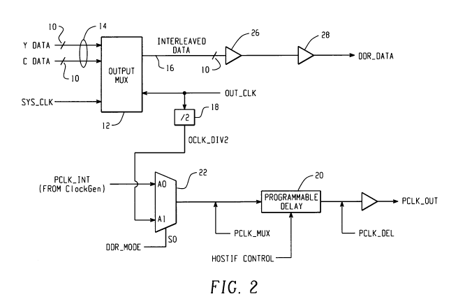
[0020] An exemplary dual data rate transmit interface (serializer) is shown in
FIG. 2.
[0021] SDI data operating at 3Gb/s is mapped in the parallel domain to a 20-
bit interface,
operating at 148.5 Mb/s. The final output stage has a multiplexer 12 for
multiplexing the 20-bit
input bus 14 to a 10-bit output bus 16 in a dual data rate mode (DDR mode or
DDR DATA).
The output bus 16 is comprised of low-voltage, CMOS compatible lines. The
output pixel clock
(PCLK OUT) is the multiplexer's output clock (OUT _CLK) divided by two by
divider 18, and
is derived from the same clock leaf as is used to clock the interleaved data
out of the output
multiplexer 12. Note that in this embodiment OUT_CLK operates internally at
297 MHz.
Multiplexer 12 may be implemented using any hardware capable of providing the
disclosed
function.
[0022] The period of each data word (running at 297 Mb/s) is 3.367 ns. This
does not allow
for much variation of output hold and delay (toh and tod, respectively) over
process, voltage and
temperature, so the circuit is designed to attempt to balance the PCLK OUT and
DDR DATA
delay as much as possible to reduce delay variation over PVT. A programmable
delay circuit 20
is placed in the PCLK_OUT path to allow finer phase adjustment, if necessary,
to compensate
for data skew on the board. This adjustment is at a resolution well below one
pixel clock period.
A multiplexer 22 selects the appropriate clock depending on whether the DDR
mode of operation
is active. Multiplexer 22 may be implemented using any hardware capable of
providing the
disclosed function.
[0023] Additional buffering of the DDR DATA is provided by buffers 26, 28 and
is done to
match the nominal default delay through the delay circuit in the PCLK_OUT
path. This delay
should be minimal, and the buffer delay should correlate quite well. Because
the PCLK_OUT
and DDR DATA pins use the same I/O cell type, the delay through the output
buffers 26, 28
should be well matched, with a result that PCLK_OUT and DDR DATA are nearly
aligned.
-5-
CA 02719955 2010-09-29
WO 2009/121186 PCT/CA2009/000434
100241 An exemplary dual data rate receive interface (deserializer) for a
transmitter is shown
in FIG. 3.
[00251 A 10-bit DDR input data bus 34 responsive to a receiver 30 operates on
both edges of
a received clock (See FIG. 1) received at a receiver 32. The input data bus 34
is comprised of
low-voltage, CMOS compatible lines. The input data bus 34 is split and sampled
in the receive
interface of the transmitter on both the positive edge of the clock by sampler
36 and the negative
edge of the incoming clock by sampler 38. The samplers 36 and 38 may be
followed by a
second sampling stage 40 at the same clock rate but this time sampling the ten
bits received on
the positive edge of the clock and the ten bits received on the negative edge
of the clock into a
twenty-bit internal data bus 42 sampled on the positive edge of the clock.
Thus, the twenty-bit
data bus 42 illustrated in FIG. 3 is reconstructed from the received ten-bit
data bus 34. The
sampling provided at 36, 38, and 40 may be provided by any known types of
hardware.
[00261 The exemplary transmitter DDR receive interface shown in FIG. 3
includes a
programmable delay circuit 44 in the clock path to accommodate a wider range
of skew on the
board and compensate for the inability of some transmitters to guarantee that
the clock and data
are aligned, with the data always lagging the clock if not perfectly aligned.
Thus, the setup and
hold window of the transmitter can be moved to prevent potential hold time
violations in the
system. This adjustment is at a resolution well below the one pixel clock
period. In case this
adjustment is used, one of the trade-offs is an increase in the size of the
setup and hold window
of the receive interface to accommodate the PVT variations that might be
introduced by the
programmable delay adjustment circuitry.
[00271 By connecting between an FPGA and a transmitter/receiver with a low pin
count data
bus, the present solution permits running the data as fast as possible for a
low-cost FPGA, and
minimizing pin usage on the FPGA, which is at a premium. Because the exemplary
parallel bus
is single-ended, the total number of required pins is I1 (10-bits data + 1-bit
pixel clock). In
addition, operating with a DDR pixel clock avoids the need to operate a high-
drive pixel clock at
297 MHz, which reduces power consumption, clock drive strength requirement,
and noise
generation. It also enables easier board routing and avoids the need of using
the higher-speed
I/Os on FPGAs, which require more expensive speed grades. Further, the LVCMOS
interface is
also simple to design with. Finally, board routing is further simplified by
the additional
-6-
CA 02719955 2010-09-29
WO 2009/121186 PCT/CA2009/000434
capability of the transmitter and receiver to change the setup/hold window and
clock to output
data delay respectively for the DDR interface.
[0028] Although the present disclosure describes a method and apparatus in
terms of one or
more embodiments, many modifications and variations are possible. For example,
one or more
steps of methods described above may be performed in a different order and
still achieve
desirable results. The following claims are intended to encompass all such
modifications and
variations.
-7-