Note: Descriptions are shown in the official language in which they were submitted.
CA 02720724 2010-10-06
WO 2009/126186 PCT/US2008/087248
1
PCT Patent Application
Practitioner Docket No. 44046.103.290.2
MANUFACTURING OF PHOTOVOLTAIC SUBASSEMBLIES
RELATED APPLICATIONS
[01] The present application is a continuation-in-part of the application
entitled:
GLAZING ASSEMBLIES THAT INCORPORATE PHOTOVOLTAIC
ELEMENTS AND RELATED METHODS OF MANUFACTURE, which has the
attorney docket number 44046.103.289.2, the serial number 12/167,826, and
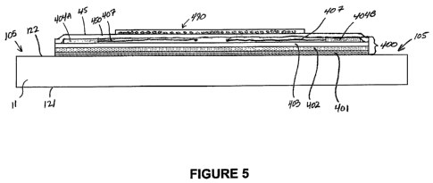
was filed on July 3, 2008, and which claims priority to the provisional
application having the serial no. 61/043,908 and being filed on April 10,
2008,
both of which are hereby incorporated by reference, in their entireties.
TECHNICAL FIELD
[02] The present invention pertains to manufacturing methods and equipment for
glazing assemblies, and the like, which incorporate photovoltaic elements.
Such assemblies, in the solar cell industry, may be more commonly known, or
referred to, as solar or photovoltaic modules or assemblies.
BACKGROUND
[03] Insulating glass (IG) units are glazing assemblies that typically include
at least
a pair of panels, or substrates, joined together such that a major surface of
one of the substrates faces a major surface of the other of the substrates,
and
an air space is enclosed between the two substrates. At least one of the
substrates is transparent, or light transmitting, and may bear a coating on
the
major surface that faces the major surface of the other substrate.
[04] With the recent renewed interest in harnessing solar power, and the
associated development of photovoltaic coatings for solar power cells, various
configurations of assemblies that incorporate photovoltaic coatings, have
been proposed. These assemblies, when configured like IG units, may be
more cost effective than traditional laminated solar panels, for example, in
that
a bulk of the material (e.g. EVA), which encapsulates the photovoltaic
coating,
in the traditional solar panel, is replaced with an air space, thereby
reducing
CA 02720724 2010-10-06
WO 2009/126186 PCT/US2008/087248
2
PCT Patent Application
Practitioner Docket No. 44046.103.290.2
material cost and manufacturing time, per unit. There is still a need for
improved methods and equipment for manufacturing assemblies, which
effectively incorporate photovoltaic coatings, in order to generate solar
power.
BRIEF SUMMARY
[05] Methods of the present invention may be used to manufacture photovoltaic
subassemblies for integration into assemblies, particularly IG unit-type
assemblies. The methods described herein are preferably suited for mass
production of assemblies in an automated, or semi-automated assembly line.
[06] Some of the inventive methods, disclosed herein, include steps for
applying a
flexible and non-electrically conductive film over a photovoltaic coating of a
first substrate, and cutting, and then aligning, with lead wires of the
photovoltaic coating, an opening, through the film, in the midst of applying
the
film. Some other methods of the present invention, alternatively, or in
addition, include steps in which desiccant beads are adhered to an adhesive
surface of sheet-like material, to form at least one desiccant sheet, and,
then,
the adhesive surface is adhered to the first substrate, such that the
desiccant
beads are held between the sheet-like material and the photovoltaic coating of
the first substrate. According to some preferred methods of the present
invention, the desiccant sheet is adhered to an exposed surface of the film
which was previously applied over the photovoltaic coating, such that the
beads are held between the sheet-like material and the film. Methods of the
present invention further include those in which desiccant sheets are formed
by causing a plurality of desiccant beads to ricochet from a plurality of
deflectors in order to bombard the adhesive surface of each discrete section
of the sheet-like material; the discrete sections are preferably drawn, from a
continuous roll of the sheet-like material, face-to-face with the deflectors
for
the bombardment with the desiccant beads. Forming of the desiccant sheets,
according to some preferred methods of the invention, takes place in an
assembly line workstation, which also applies the sheets to each first
substrate that enters the workstation.
CA 02720724 2010-10-06
WO 2009/126186 PCT/US2008/087248
3
PCT Patent Application
Practitioner Docket No. 44046.103.290.2
[07] The present disclosure further includes inventive manufacturing apparatus
embodiments that may be included in an assembly line to carry out methods
of the present invention. According to some embodiments of the present
invention, a manufacturing apparatus includes means for forming desiccant
sheets from a continuous roll of sheet-like material, for example, according
to
the method, which is outlined in the latter portion of the preceding
paragraph.
BRIEF DESCRIPTION OF THE DRAWINGS
[08] The following drawings are illustrative of particular embodiments of the
present invention and therefore do not limit the scope of the invention. The
drawings are not to scale (unless so stated) and are intended for use in
conjunction with the explanations in the following detailed description.
Embodiments of the present invention will hereinafter be described in
conjunction with the appended drawings, wherein like numerals denote like
elements.
[09] Figure 1 is a perspective view of an exemplary IG-unit type assembly.
[10] Figure 2 is a schematic plan view of either of the substrates of the
assembly
shown in Figure 1.
[11] Figure 3 is a perspective view of a portion of the assembly shown in
Figure 1.
[12] Figure 4 is a cross-section view through section line A-A of Figure 1.
[13] Figure 5 is a cross-section of a portion of the assembly shown in Figure
4,
which may be assembled according to some methods of the present
invention.
[14] Figure 6 is a schematic representation of an assembly line, according to
some
embodiments of the present invention.
[15] Figure 7A is a perspective view of a workstation, which may be
incorporated
into the assembly line of Figure 6, according to some embodiments of the
present invention.
CA 02720724 2010-10-06
WO 2009/126186 PCT/US2008/087248
4
PCT Patent Application
Practitioner Docket No. 44046.103.290.2
[16] Figure 7B is an enlarged, detailed view of a portion of the workstation
shown
in Figure 7A, according to some embodiments.
[17] Figures 8A-C make up a series of schematics, which depict some of the
steps
of a method carried out by the workstation of Figures 7A-B.
[18] Figure 9A is a perspective view of another workstation, which may be
incorporated into the assembly line of Figure 6, according to some
embodiments of the present invention.
[19] Figure 9B is a view into a chamber of the workstation shown in Figure 9A,
according to some embodiments.
[20] Figure 9C is a top view schematic, which portrays an operation of the
workstation shown in Figures 9A-B, according to some embodiments.
[21] Figure 10 is a perspective view of a portion of the workstation of Figure
9A,
separated from the rest of the workstation, according to some embodiments.
[22] Figure 11 is a plan view of a portion of a photovoltaic subassembly,
according
to some methods and embodiments of the present invention.
DETAILED DESCRIPTION
[23] The following detailed description is exemplary in nature and is not
intended
to limit the scope, applicability, or configuration of the invention in any
way.
Rather, the following description provides practical illustrations for
implementing exemplary embodiments of the present invention.
[24] Figure 1 is a perspective view of an exemplary IG-unit type assembly 10.
Figure 1 illustrates assembly 10 including a first substrate 11, a second
substrate 12 and a seal system 15, which joins substrates 11, 12 together; a
first major surface 121 of each of substrates 11, 12, face outward or away
from one another, and a second major surface 122 of each of substrates 11,
12 faces inward, or toward one another, being spaced apart from one another
by a seal system 15. Figure 2 is a schematic plan view of either of the
substrates 11, 12 of assembly 10. Figure 2 illustrates second, or inner major
CA 02720724 2010-10-06
WO 2009/126186 PCT/US2008/087248
PCT Patent Application
Practitioner Docket No. 44046.103.290.2
surface 122 of substrate 11,12 having a central region 103 and a peripheral
region 105, which are delineated from one another by the dashed line.
According to the illustrated embodiment, seal system 15 joins first substrate
11 to second substrate 12 along peripheral regions 105 of inner major
5 surfaces 122. Figure 3 is a perspective view of assembly 10, having second
substrate 12 removed to show an air space 200 that is enclosed between
substrates 11, 12 when they are joined together by seal system 15.
[25] Figure 3 further illustrates seal system 15 having a thickness t, so as
to
maintain airspace 200; thus, seal system 15 further serves as a spacer
member between substrates 11,12. According to some embodiments,
thickness t is between approximately 0.01 inch and approximately 0.1 inch,
preferably approximately 0.04 inch, but could be up to 1.5 inches in alternate
embodiments. According to some embodiments, seal system 15 is formed, at
least in part, from a polymer material, for example, a thermoplastic, such as
a
Kommerling TPS, having low moisture vapor transmission properties, for
example, resulting in a moisture vapor transmission rate (MVTR)
therethrough, which does not exceed approximately 20 g mm/m2/day. Other
examples of these polymer materials include, without limitation, butyl rubber,
ionomers, ethylene methacrylic acid copolymers and polyisobutylenes, the
ethylene methacrylic acid copolymers being preferred for their excellent
adhesion properties, which are desirable to hold together assemblies such as
assembly 10. Some examples of these preferred materials, which are
commercially available, are Sentry Glas Plus, available from DuPont, and
PRIMACORTM, available from Dow Chemical.
[26] According to some preferred embodiments, seal system 15 includes a first
member 151, which extends along an inner portion of peripheral region 105,
and a second member 152, which extends about an external perimeter of first
member 151, along an outer portion of perimeter region 105, for example as
illustrated in Figure 4. Figure 4 is a section view through section line A-A
of
Figure 1. With reference to Figure 4, first member 151 may be affixed to
opposing peripheral regions 105 of inner major surfaces 122 of substrates 11,
CA 02720724 2010-10-06
WO 2009/126186 PCT/US2008/087248
6
PCT Patent Application
Practitioner Docket No. 44046.103.290.2
12, in order to join substrates 11, 12 to one another, leaving an outer
perimeter channel between the outer portions of the opposing peripheral
regions 105 to be later filled with second member 152. First member 151 is
preferably formed from a polymer material, which has low moisture vapor
transmission properties, for example, any of those referenced above; and
second member 152 may be formed of any material having suitable adhesive
properties, for example, silicone, polysulfide or polyurethane. Some
commercially available silicone adhesives, which are suitable for second
member 152, include, without limitation, 3-0117 silicone insulating sealant
and
995 silicone structural sealant from Dow Corning, IGS 3729 sealant from
Momentive Performance Materials (formerly GE Silicones), and SikaGlaze
sealants (IG -16, IG-25 and IG 25HM) from the Sika Corporation. Both
members 151, 152 preferably provide for sealing and adhesion between
substrates 11, 12, and at least first member 151 also serves as a spacer
member, but, according to some alternate embodiments, first member 151
may serve solely as a spacer member and second member 152 solely as a
sealing and adhesive member.
[27] According to some preferred embodiments, first substrate 11 is light
transmitting, for example, formed from glass or a plastic material, such as
polycarbonate, and second substrate 12 may be similarly formed or may be
opaque. According to some alternate embodiments, second substrate is light
transmitting, for example, formed from glass or a plastic material, such as
polycarbonate, and first substrate 11 may be similarly formed or may be
opaque. Figure 4 further illustrates assembly 10 including a photovoltaic
coating 400 extending over, and being adhered to, inner major surface 122 of
first substrate 11, and a flexible and electrically non-conductive film 450
extending over photovoltaic coating 400, such that coating 400 is sandwiched
between substrate 11 and film 450, and airspace 200 is located between an
exposed surface 45 of film 450 and second substrate 12.
[28] Film 450 may be formed, preferably pre-formed, prior to application over
coating 400, from a polyolefin material, for example, a polyethylene or
CA 02720724 2010-10-06
WO 2009/126186 PCT/US2008/087248
7
PCT Patent Application
Practitioner Docket No. 44046.103.290.2
polypropylene, or from a polyester material, and may have a thickness
between approximately 0.001 inch and approximately 0.015 inch, preferably
approximately 0.0035 inch. According to some preferred embodiments, film
450, when pre-formed, includes an adhesive backing 421 for adhering film
450 to coating 400, and may be supplied in rolls. Adhesive backing 421 may
be formed by an acrylic adhesive or by a rubber-based adhesive, or by any
other suitable adhesive known to those skilled in the art, and may extend over
approximately an entirety of the interface between film 450 and coating 400 or
just over selected portions of the interface. Alternatively, film 450 may be
otherwise secured over coating 400, for example, a perimeter of film 450 may
be captured between a portion of seal system 15 and first substrate 11. It
should be noted that film 450 may extend only over coating 400, or may
significantly extend into peripheral region 105, even as far as to cover an
entirety of major surface 122; alternatively, film 450 may leave some portions
of coating 400 uncovered, for example, in close proximity to the perimeter
edges thereof.
[29] According to embodiments of the present invention, substrate 11,
photovoltaic
coating 400 and flexible and electrically non-conductive film 450 form a
photovoltaic panel of assembly 10 so that assembly 10 can function as a solar
power cell. Photovoltaic coating 400 may be of any type known to those
skilled in the art, either of the conventional type, for example, including an
array of silicon wafers interconnected by soldered conductors, or of the `thin
film' type, for example, including several thin film semiconductor layers,
which
are patterned to form electrically interconnected cells. An embodiment of the
present invention, which includes coating 400 as a thin film CdTe type will be
described, below, in conjunction with Figure 5, however, it should be
appreciated that alternate embodiments may incorporate coating 400 as a thin
film Cu(InGa)Se2 (GIGS) type or amorphous silicon(a-Si) type.
[30] Because film 450 is enclosed between first and second substrates 11, 12
of
assembly 10, film 450 need not have a durability that is otherwise required
for
exposed polymer back skins employed by some photovoltaic panels known in
CA 02720724 2010-10-06
WO 2009/126186 PCT/US2008/087248
8
PCT Patent Application
Practitioner Docket No. 44046.103.290.2
the art. However, according to some preferred embodiments, film 450 has
properties such that the integrity of film 450 is maintained under thermal
cycling conditions, for example, temperatures ranging between approximately
- 400C and approximately 85 C, over a life span of up to, and preferably
exceeding, approximately 20 years.
[31] With further reference to Figure 4, according to some preferred
embodiments,
a desiccant sheet 490 is adhered to exposed surface 45 of film 450, within
airspace 200, in order to absorb any moisture that may pass through seal
system 15. Desiccant sheet 490 is formed from a sheet-like material 492 to
which a plurality of desiccant beads 493 are adhered, such that beads 493
are held between sheet-like material 492 and exposed surface 45 of film 450.
All, or portions of, surface 45 of film 450 may be treated to improve adhesion
of sheet-like material 492 thereto, for example, by a plasma process such as
a corona treatment, either prior to, or following, adhering film 450 to
coating.
Sheet-like material 492 allows moisture transmission therethrough, for
absorption by desiccant beads 493, and may be formed of the same, or
similar, material from which film 450 is formed. Sheet-like material 492 may
be pre-formed with an adhesive backing, for example, as described above for
film 450, and may be supplied in rolls. The size of the area of exposed
surface 45 that desiccant sheet 490 covers is determined, in order to provide
the desired moisture absorption for the particular assembly, according to a
volume of air space 200, and a density of plurality of desiccant beads 493,
for
a particular type of desiccant sheet 490. According to an exemplary
embodiment, approximately 50 grams of 3 A molecular sieve beaded
desiccant, 0.8 mm to 1 mm in size, and having a minimum absorption capacity
of 19%, by weight, is included for an airspace having a volume of
approximately 720 cubic centimeters. The sheet-like material, to which this
amount of beaded desiccant is adhered, is preferably a polyethylene film that
includes an acrylic adhesive backing, and has a footprint of approximately 180
square inches (1150 cm2). According to some preferred embodiments,
plurality of beads 493 are adhered to a central region of sheet-like material
CA 02720724 2010-10-06
WO 2009/126186 PCT/US2008/087248
9
PCT Patent Application
Practitioner Docket No. 44046.103.290.2
492, leaving a peripheral region free of beads for securing desiccant sheet
490 to surface 45.
[32] According to some alternate embodiments, surface 45 of film 450 may
include
an adhesive layer such that desiccant beads 493 may be adhered directly
thereto, with or without sheet-like material 492 extending over beads 493; or
sheet-like material 492 may include an adhesive backing on both sides
thereof, so that the side to which beads 493 are adhered faces outward from
film 450 and the opposing side is adhered to surface 45 of film 450.
According to yet further embodiments, desiccant sheet 490 is adhered to
second substrate 12, or an alternative form of desiccant may be provided
within airspace 200, for example, either embedded in a polymer matrix, or
packaged in a sack, or `free-floating' in airspace 200, or otherwise present
in
airspace 200. The desiccant material, according to any of the above-
described embodiments, in combination with the aforementioned relatively low
MVTR of seal system 15, may prevent moisture build-up within airspace 200
that can lead to corrosion of certain elements of photovoltaic coating 400.
[33] Figure 5 is a cross-section of the photovoltaic panel portion of the
assembly
shown in Figure 4, by which a non-limiting example of coating 400 is
presented. Figure 5 illustrates coating 400 including a first layer 401, which
may be formed by a transparent conductive oxide (TCO), for example,
comprising Tin oxide (Sn02); first layer 401 may be overlaid with a
semiconductor layer 402, for example, comprising two `sub-layers': Cadmium
sulfide (CdS; `window' layer; n-type), extending adjacent to first layer 401,
and
Cadmium Telluride (CdTe; absorbing layer; p-type), overlaying the Cadmium
sulfide sub-layer. Figure 5 further illustrates an electrical contact layer
403,
for example, comprising nickel, which extends between the Cadmium
Telluride sub-layer of semiconductor layer 402, and a pair of bus bars 404A,
404B. Bus bars 404A, 404B may each be formed from a copper tape, for
example, approximately 0.003 - 0.007 inch thick, which are adhered to contact
layer 403, for example, by a conductive acrylic adhesive. Bus bars 404A,
404B preferably extend approximately parallel to one another along opposing
CA 02720724 2010-10-06
WO 2009/126186 PCT/US2008/087248
PCT Patent Application
Practitioner Docket No. 44046.103.290.2
edge portions of coating 400; an internal insulated conductor 407 is coupled
to each bus bar 404A, 4046, and conductors 407 may terminate near an
electrical access, or feedthrough, opening 480 in film 450 (Figure 3). Film
450
can provide additional retention for holding bus bars 404A, 404B in intimate
5 contact with contact layer 403 and for securing insulated conductors 407
against layer 400. An electrical lead 420, which is shown in Figures 1, 3 and
4, includes a pair of isolated conductive lead wires to collect power from the
photovoltaic panel; each wire of lead 420 is coupled to a corresponding
conductor 407, for example, via soldering to a respective terminal thereof in
10 proximity to opening 480. If opening 480 is not provided, conductors 407
may
terminate in proximity to a perimeter edge of film 450, for coupling to lead
420.
[34] With reference to Figure 1, second substrate12 is shown including an
opening
18, which may be approximately aligned with feedthrough opening 480, and
extends through second substrate 12, to allow passage of lead 420 out from
assembly 10. A diameter of openings 480, 18 may be between approximately
1/4 inch and approximately 1 inch. According to the illustrated embodiment,
after routing lead 420 out from system 10, through opening 18, a potting
material is applied around lead 420, to seal off opening 18. Examples of
suitable potting materials include, without limitation, polyurethane, epoxy,
polyisobutylene, and any low MVTR material. According to alternate
embodiments, opening 480 is not necessary, and lead 420 extends out from
assembly 10 through an opening in seal system 15 or through an opening
between seal system 15 and one of substrates 11, 12, or through an opening
in first substrate 11.
[35] According to some preferred embodiments of the present invention, the
flexibility of film 450, in combination with a tear strength thereof, is
suited to
hold substrate 11 and photovoltaic coating 400 together, in case substrate 11
is fractured, thereby containing fragments of the fractured substrate 11 to
prevent a scattering of potentially toxic elements of photovoltaic coating
400,
for example, Cadmium. Furthermore, in the event that substrate 12 is broken,
the electrical insulating property of film 450 preferably electrically
isolates
CA 02720724 2010-10-06
WO 2009/126186 PCT/US2008/087248
11
PCT Patent Application
Practitioner Docket No. 44046.103.290.2
coating 400 and electrically charged conductors 407, which are coupled to
bus bars 404A,B of coating 400, thereby preventing potential injury to one
handling the broken assembly. Film 450 may further protect the
semiconductor sub-layers of coating 400 if, for example, during relatively
cold
temperature conditions, the air space between substrates 11, 12 shrinks such
that substrates 11, 12 come into contact. According to some embodiments,
in which sun light is received by coating 400 through first substrate 11, for
example, in the case of the CdTe type of coating (Figure 5), and second
substrate 12 is translucent or transparent, flexible film 450 is opaque to
provide a more aesthetically pleasing uniform appearance to the photovoltaic
panel, when viewed through second substrate 12. According to those
embodiments in which coating 400 is the CIGS type, since sun light is
received by the coating 400 through second substrate 12 and through film
450, film 450 needs to light transmitting.
[36] Figure 6 is a schematic layout for an assembly line 60, according to some
embodiments, which carries out some methods of the present invention.
Many or all of the workstations included in assembly line 60 may be
automated, or semi-automated, to carry out some or all of the methods that
are described below. Figure 6 illustrates a flow of line 60 from left to
right,
but, it should be noted that, the flow could be in the opposite direction,
according to alternate embodiments. It should be understood that a plurality
of first substrates, which each have a photovoltaic coating pre-formed
thereover, for example, like photovoltaic coating 400 (Figure 4) formed over
central region 103 of major surfacel 22 (Figure 2) of first substrate 11, are
fed
sequentially into line 60, starting at a workstation 700. Each pre-formed
photovoltaic coating preferably extends over the central region of the major
surface of the corresponding first substrate, without significantly
encroaching
on a peripheral region of the surface, for example, region 105 (Figures 2 and
5), so as to maintain exposure of a native surface of each substrate for
fixation to a corresponding sealing system, for example, sealing system 15.
The sealing system, according to some preferred embodiments, serves as
CA 02720724 2010-10-06
WO 2009/126186 PCT/US2008/087248
12
PCT Patent Application
Practitioner Docket No. 44046.103.290.2
both a spacer, between substrates, and as a seal, having low moisture vapor
transmission properties, for example, resulting in a moisture vapor
transmission rate (MVTR) therethrough, which does not exceed approximately
20 g mm/m2/day moisture, as described above. With reference to Figure 6, a
first member of the sealing system, for example, first member 151, as
described above, is applied to each first substrate at a workstation 900,
after a
sheet of flexible and electrically non-conductive film, for example, film 450
(Figures 4-5), is overlaid onto the corresponding photovoltaic coating, at
workstation 700, and after a desiccant sheet, for example, sheet 490 (Figures
4-5), is overlaid onto the corresponding film, at a workstation 800. Work
stations 700 and 800 will be described in greater detail, below, in
conjunction
with Figures 7A-10.
[37] Figure 6 further illustrates a feeder station 925, which sequentially
brings each
of a plurality of second substrates, for example, like second substrate 12
(Figures 1, 2 and 4), to a station 950, where each second substrate is brought
face-to-face with a corresponding first substrate, which has been processed in
workstations 700, 800 and 900. At station 950, each pair of first and second
substrates are brought face-to-face, such that a peripheral region of each is
approximately aligned, with one another, and then each pair is conveyed,
downstream, to a workstation 1000. Prior to bringing the substrates of each
pair together, an opening, for example, opening 18 (Figure 1), may be formed
in the second substrate, for example, at station 925, or upstream thereof. If
the opening is formed in each second substrate, the opening is preferably
aligned with an opening in the film of the corresponding first substrate, for
example, feedthrough opening 480 (Figure 3), when the substrates are
brought together.
[38] At workstation 1000 each pair of first and second substrates is pressed
together, for example, by confronting platens, with the first (spacer/seal)
member sandwiched therebetween, so that the member extends along the
peripheral regions of the facing major surfaces, while maintaining an air
space, for example air space 200 (Figure 4), between the central regions of
CA 02720724 2010-10-06
WO 2009/126186 PCT/US2008/087248
13
PCT Patent Application
Practitioner Docket No. 44046.103.290.2
the facing major surfaces of the first and second substrate pair. Although not
necessary, heat may be applied, along with pressure, in workstation 1000, to
securely affix the spacer/seal member to each of the substrates.
[39] With further reference to Figure 6, assembly line 60 includes a series of
workstations 1050 that are located downstream of workstation 1000, where
secondary processes, related to the photovoltaic coating of each assembly,
are performed. For example, at a first of workstations 1050, an external lead
is coupled to conductor wires of each photovoltaic coating. The lead may
extend though an opening in second substrate, for example, like lead 420
(Figures 1, 3 and 4), as previously described. At a subsequent workstation of
series 1050, a potting material is applied around the lead at the opening, to
seal off the opening, as was also as previously described; the potting
material
may further form a strain relief for the lead adjacent to the second
substrate,
or a separate strain relief member may be installed about the lead.
Workstations 1050 may further include one or more electrical test/inspection
stations, for example, located downstream of that in which the potting
material
is applied.
[40] Finally, a second member, for example, second member 152, of the seal
system, for each assembly formed in line 60, is applied about an external
perimeter of the first member, in between the first and second substrates, at
a
workstation 1250. According to some preferred embodiments, the second
member is silicone adhesive, and Figure 6 schematically illustrates a wall
that
separates workstation 1250 from the rest of assembly line 60, in order to
isolate those assemblies, which are being processed upstream of workstation
1250, from potential silicone contamination.
[41] Figure 7A is a perspective view of workstation 700, according to some
embodiments; and Figure 7B is an enlarged, detailed view of a portion of the
workstation 700, according to some embodiments. Figure 7A illustrates a
conveyer belt 72 for conveying first substrates, per arrow A, one at a time,
past a film application work head 705 of workstation 700. First substrate 11
is
CA 02720724 2010-10-06
WO 2009/126186 PCT/US2008/087248
14
PCT Patent Application
Practitioner Docket No. 44046.103.290.2
shown being conveyed on conveyor belt 72 and supported in an upright
orientation, by sets of rollers 722, which are positioned along a length of
conveyer belt 72. The upright orientation of first substrate 11 is such that a
pre-formed photovoltaic coating, for example, photovoltaic coating 400 (Figure
4), which is adhered to a major surface of first substrate 11, faces work head
705 and extends from a first elevation El to a second elevation E2. Figure 7A
further illustrates a continuous roll of film 75 mounted, for example, on a
spindle, in proximity to work head 705, so that work head 705 may draw
discrete sections of the film, from roll 75, in order to apply each section
over
photovoltaic coating 400, of each first substrate 11, as coating 400 is
conveyed past work head 705, and to separate each section from the
remainder of the film. The film from roll 75 is a flexible and electrically
non-
conductive film, which, preferably, includes an adhesive backing, for example,
and of the previously-described embodiments of film 405.
[42] According to some preferred methods, an opening, for example, the
previously-described feedthrough opening 480 (Figure 3), is formed in each
discrete section of the film in the midst of applying the section to
photovoltaic
coating 400. With reference to Figures 7A-B, workstation 700 is shown
including a cutting tool 78, which is positioned between roll of film 75 and
film
application work head 705. Figure 7B illustrates cutting tool 78 including a
pair of blades 782 and a disk 781, the operation of which will be described in
greater detail, below. According to some alternate methods, an opening may
be pre-formed in each discrete section of the film prior to loading roll of
film 75
into workstation 700.
[43] Figures 8A-C make up a series of top-view schematics, which outline a
method of operation of workstation 700. Figure 8A illustrates a first terminal
edge 81 of the film having been pulled away from roll 75, and a first edge 841
of photovoltaic coating 400 of first substrate 11 having been moved into
proximity with first terminal edge 81 of the film, at a first position 1, for
initial
contact therewith. With reference back to Figure 7A, in conjunction with
Figure 8A, continuous roll of film 75 is initially loaded into workstation
700,
CA 02720724 2010-10-06
WO 2009/126186 PCT/US2008/087248
PCT Patent Application
Practitioner Docket No. 44046.103.290.2
such that first terminal edge 81 extends between first and second elevations
El, E2, at first position 1, in order to be located for the initial contact
with first
substrate 11. With further reference to Figure 7A, a width W of film is
defined
by first terminal edge 81, which, in Figures 8A-C, extends into the page.
5 Arrow A, in Figure 8A, indicates a generally horizontal direction in which
substrate 11 and coating 400, being adhered thereto, are conveyed, from first
position 1, to a second position 2, which is shown in Figure 8B.
[44] With reference to Figure 8B, the movement of coating 400, to second
position
2, draws a first portion 801 of the film into adhesive contact with coating
400.
10 Figures 8A-B illustrate a pinch roller 851, which, in conjunction with
conveyor
belt 72 (Figure 9A), drives substrate 11, per arrow A, to move coating 400;
another roller 853 is shown supporting substrate 11, on an opposite side from
pinch roller 851. Figure 8B illustrates first edge 841 of coating 400 being
held
stationary at second position 2, while cutting tool 78 cuts an opening through
15 a second portion 802 of the film, which second portion 802 extends from
first
portion 801 toward roll 75. With reference back to Figure 7B, in conjunction
with Figure 8B, disk 781 of cutting tool 78 is moved toward the film and pair
of
blades 782, which are located on an opposite side of the film, in order to
hold
the film steady, while blades 782 rotate, to cut out the opening in second
portion 802 of the film; a diameter of disk 781 preferably fits within a
spacing
between blades 782. According to some preferred embodiments, cutting tool
78 further includes a vacuum source connected to disk 781 for keeping the
cut out portion of the film from falling; the vacuum may subsequently be
released, as second portion 802 of the film is drawn alongside disk 781, so
that the cut out portion may be stuck onto the facing surface of the film
downstream of the opening.
[45] With reference to Figure 8C, after the opening is cut, first edge 841 of
coating
400 is moved, again per arrow A, in the generally horizontal direction, to a
third position 3, in order to draw second portion 802 of the film into
adhesive
contact with coating 400. The opening formed in second portion 802 should
be approximately aligned with lead wires, for example, wires 407 (Figure 5),
of
CA 02720724 2010-10-06
WO 2009/126186 PCT/US2008/087248
16
PCT Patent Application
Practitioner Docket No. 44046.103.290.2
photovoltaic coating 400, in order to provide a feedthrough opening for the
wires.
[46] Figure 8C illustrates another cutting tool 79, located within film
application
work head 705 to cut and, thereby, create a second terminal edge 82 of the
film, which extends along the width W of the film (Figure 7A); the cut
separates a third portion 803 of the film from a remainder of the film on roll
75.
Third portion of film 803 extends from second portion 802 and will be drawn
into adhesive contact with coating 400, as a second edge 842 of coating 400,
which is opposite first edge 841, is moved into proximity with first position
1.
[47] Once third portion 803 of the film has been adhered to coating 400, the
application of the film over coating 400 of first substrate 11 is complete so
that
the applied film generally corresponds to film 450 of the above-described
embodiments, for example, a illustrated in Figures 4 and 5. As previously
described, the film is adhered to photovoltaic coating 400 by means of an
adhesive backing, which is preferably pre-formed on a surface of the film.
The adhered film preferably covers an entirety of the photovoltaic coating on
first substrate 11, while leaving enough of peripheral region 105 of surface
122 (Figure 2) free for joining the first substrate to the second substrate,
as
previously described. However, according to some embodiments, the
footprint of the adhered film may leave a portion of a perimeter of coating
400
uncovered.
[48] Figure 9A is a perspective view, including a cut-away section, of
workstation
800, according to some embodiments of the present invention; workstation
800 is adapted to both form and apply a desiccant sheet, for example, like
desiccant sheet 490, to the exposed surface of the film of each first
substrate,
for example, film 450 of substrate 11, which is conveyed from workstation
700. Figure 9A illustrates work station 800 including a desiccant bead
applicator assembly 860 and a desiccant sheet application work head 805,
which applies a discrete section of sheet-like material to each first
substrate
11, in manner similar to that described, above, for each section from
CA 02720724 2010-10-06
WO 2009/126186 PCT/US2008/087248
17
PCT Patent Application
Practitioner Docket No. 44046.103.290.2
continuous roll of film 75, in workstation 700; a continuous roll of adhesive-
backed sheet-like material 85, for example, mounted on a spindle, is shown
positioned in proximity to a chamber 82 of applicator assembly 860.
According to the illustrated embodiment, conveyor belt 72 conveys first
substrates 11, from workstation 700, past desiccant sheet application work
head 805; as each first substrate 11 passes work head 805, the
corresponding discrete section of the sheet-like material, from continuous
roll
85, which has been formed into a desiccant sheet by applicator assembly
860, is brought into adhesive contact with the surface of the film, for
example,
surface 45 of film 450, that overlays photovoltaic coating 400 of each first
substrate 11. Some methods of the present invention integrate a surface
treatment process into assembly line 60, for example, between workstations
700 and 800, in order to treat the surface of the film, for improved adhesion
of
the desiccant sheet thereto. The treatment process may be a plasma type,
for example, a corona treatment, which raises the surface energy of the
surface of the film. Equipment and methods suitable for such a surface
treatment process are known to those skilled in the art.
[49] Figure 9A further illustrates desiccant bead applicator assembly 860
including
a hopper 81, which holds and dispenses desiccant beads 89 (seen via the
cut-away section through hopper 81), into chamber 82, which is positioned
below hopper 81, to receive the dispensed beads 89, that fall, under the force
of gravity, from hopper 81, for the application of the beads to the sections
of
the sheet-like material, as the sections pass through chamber 82. According
to the illustrated embodiment, desiccant beads 89 that fall from hopper 81
into chamber 82, are deflected by a plurality of deflectors 822, which are
shown in the view within chamber 82 of Figure 9B. Figure 9B illustrates
deflectors 822 being formed as wedges, which are mounted to a plate 820,
such that a deflection surface 832, of each deflector 822, is positioned below
hopper 81 and slants downward, and away from plate 820. Figure 9B further
illustrates a rotating framework 825, which surrounds deflectors 822 and plate
820, and which includes spaced-apart struts 815, against which the adhesive-
CA 02720724 2010-10-06
WO 2009/126186 PCT/US2008/087248
18
PCT Patent Application
Practitioner Docket No. 44046.103.290.2
backed side of sheet-like material, from roll 85, is drawn, so as to bring
each
discrete section, of the adhesive-backed side, which spans a pair of adjacent
struts 815, face-to-face with deflectors 822. The falling beads ricochet,
being
deflected laterally from surfaces 832, to bombard the facing adhesive surface
of each section of the sheet-like material.
[50] Figure 9C is a top view schematic showing an exemplary path of the sheet-
like material from roll 85, wherein each discrete section thereof, which is
formed into a desiccant sheet 490A-D, is generally delineated. Figure 9C
illustrates the sheet-like material passing into contact with framework 825,
which rotates, per arrow B, as the material is drawn through chamber 82, for
example, by the movement, per arrow A of substrate 11, which may be driven
by conveyor belt 72 (Figure 9A) and pinch roller 851, as was previously
described for workstation 700. According to some embodiments, framework
825 may be actively rotated, for example, via a coupling to a motor, to draw
the sheet-like material, either as an alternative to the movement of substrate
11, or in addition thereto. In any case, the mechanism for drawing the sheet-
like material, from continuous roll 85, into contact with framework 825 and,
then, into adhesive contact with surface 45, preferably, should not stretch
the
material.
[51] A spacing S between each pair of adjacent struts 815 of framework 825
effectively forms an aperture, through which desiccant beads, which have
fallen from hopper 81, and which ricochet from surfaces 832 of deflectors 822,
bombard the adhesive-backed side of the sheet-like material, to form each
desiccant sheet 490A-D. With further reference to Figure 9B-C, a thickness
of each strut 815 serves to shield opposing peripheral portions of each
section
of the sheet-like material to keep these portions desiccant-free. Dashed lines
in Figure 9B indicate optional additional cross-members extending between
each pair of adjacent struts 815; these cross-members may provide shielding
of additional opposing peripheral portions of the adhesive-backed surface of
each desiccant sheet 490A-D. Either extent of the desiccant-free portions
may facilitate adhesion of sheets 490A-D to the corresponding surface 45 of
CA 02720724 2010-10-06
WO 2009/126186 PCT/US2008/087248
19
PCT Patent Application
Practitioner Docket No. 44046.103.290.2
film 450 of each first substrate 11, such that the adhered desiccant beads are
held between surface 45 of film 450 and the corresponding section of sheet-
like material.
[52] Figure 10 is a perspective view of a portion of workstation 800, shown
separated from the rest of workstation 800, according to some embodiments.
Figure 10 illustrates deflection surfaces 832, of deflectors 822, facing
generally upward, toward hopper 81, so that the plurality of desiccant beads
89 (Figure 9A) that fall from hopper 81, per arrow D, will ricochet off
surfaces
832. Figure 10 further illustrates plate 820 including a plurality of mounting
features 821, which are formed by holes in the surface of plate 820, for the
attachment of deflectors 822 to plate 820. According to the illustrated
embodiment, each deflector 822 may include one or a number of threaded
bores, for example, formed in a face thereof that is opposite deflection
surface
832; the one or more bores may be sized to receive a mating threaded
fastener that extends through features 821 of plate 820. Alternately, each
deflector may include one or a number of protruding pegs, which extend
therefrom, for example, along the face opposing deflection surface 832, and
are sized to snuggly fit within mounting features 821. According to an
exemplary embodiment, the wedges, which form deflectors 822, each have a
thickness of approximately 0.5 inch, and a depth d and a height h of
approximately 1.5 inch; the illustrated arrangement of deflectors 822 may be
suitable for applying the aforementioned 50 grams of 3 A molecular sieve
beaded desiccant, 0.8 mm to 1 mm in size, to the adhesive-backed surface of
each desiccant sheet 490A-D (Figure 9C), when a footprint of each sheet is
approximately 180 square inches (1150 cm2).
[53] According to some preferred embodiments, the number, configuration and
arrangement of features 821, of plate 820, and the aforementioned mating
fasteners, or pegs, may allow for a re-arrangement of deflectors 822 along the
surface of plate 820, within workstation 800. The ability to re-arrange
deflectors 822 may provide a flexibility for workstation 800 to handle the
application of a variety of types of desiccant beads, and/or to provide a
variety
CA 02720724 2010-10-06
WO 2009/126186 PCT/US2008/087248
PCT Patent Application
Practitioner Docket No. 44046.103.290.2
of desiccant bead bombardment patterns according to particular moisture
absorption requirements for various types of assemblies.
[54] Referring back to Figure 9A, a conduit 810 is shown extending, from below
chamber 82, up to a bin 83, which is adjacent to, and in fluid communication
5 with, hopper 81. According to the illustrated embodiment, an excess quantity
of desiccant beads, which do not adhere to the adhesive surface of the sheet-
like material, are re-circulated from chamber 82, through conduit 810, back to
hopper 81. According to some embodiments, a series of disks, which are
attached to a cable, that extends within conduit 810, are lifted by the cable,
10 like elevators, to carry the beads up into bin 83; according to some
alternate
embodiments, a vacuum is applied within conduit 810, to draw the beads up
into bin 83. Preferably, a filtering system is included in workstation 800, to
prevent dust, that may be formed during bead re-circulation, from entering
hopper 81.
15 [55] It should be noted that alternative methods are contemplated for
applying
desiccant to each first substrate. For example, workstation 800 may be
eliminated from assembly line 60, and desiccant bead applicator assembly
860 incorporated into workstation 700. According to this alternative, film
from
roll 75 may be adhesive-backed on both sides and drawn through assembly
20 860 so that the desiccant beads bombard one of the sides; then the film may
be applied to the first substrate, for example, according to the method
described above for workstation 700, so that the opposite side of the film
adheres to the photovoltaic coating on the first substrate, and the side, to
which the beads are adhered, faces outward from the coating. If workstation
800 remains in assembly line 60, it may simply function to apply a section of
sheet-like material over the desiccant beads, that are adhered to outward-
facing surface of the adhered film; otherwise the desiccant beads are left
exposed within the airspace that is subsequently formed between the first
substrate and the second substrate, when the two substrates are brought
together.
CA 02720724 2010-10-06
WO 2009/126186 PCT/US2008/087248
21
PCT Patent Application
Practitioner Docket No. 44046.103.290.2
[56] After desiccant is applied to first substrate 11, first substrate 11 is
conveyed to
workstation 900 (Figure 6) for the application of a first member of a seal
system, for example, first member 151 of seal system 150, described above;
first member 151, which preferably serves as a spacer and a sealing member,
is applied to peripheral region 105, of first substrate 11, which surrounds
photovoltaic coating 400. Figure 11 is a plan view of first substrate 11, upon
application of first member 151 of seal system 150. According to some
preferred methods, substrate 11 is conveyed, in the upright orientation, that
is
illustrated in Figure 7A, on conveyer belt 72, into workstation 900 where
member 151 is applied. Member 151 may be preformed, essentially in the
shape shown in Figure 11, prior to application thereof to substrate 11, or,
preferably, extruded, for example, from a nozzle that is mounted in
workstation 900.
[57] After first member 151 is applied to first substrate 11, first substrate
11 is
conveyed, preferably still in the same upright orientation, to station 950,
where
second substrate 12 is moved from station 925, into alignment with first
substrate 11, as described above, in conjunction with Figure 6. As was also
described above, substrates 11, 12 are pressed together, for example, by
confronting platens, such that member 151 joins the substrates, maintains an
airspace therebetween, and seals the airspace.
[58] Figure 11 further illustrates feedthrough opening 480 in film 450, by
which
electrical lead wires 470 (Figure 5) of photovoltaic coating 400 are accessed
for coupling to a lead, for example, lead 420 (Figures 1, 3 and 4), as
previously described. Once substrates 11, 12 are joined together, access to
feedthrough opening 480 may be obtained, for example, through opening 18
(Figure 1) in substrate 12, for the coupling of lead 420 to wires 460.
[59] Finally, following the coupling, and other related operations that take
place in
workstations 1050, as described above, a second member of the seal system,
for example, second member 152, is applied, at workstation 1250, within a
channel, that is left between outer portions of the facing peripheral regions
CA 02720724 2010-10-06
WO 2009/126186 PCT/US2008/087248
22
PCT Patent Application
Practitioner Docket No. 44046.103.290.2
105 of joined substrates 11, 12, to extend about an external perimeter of
first
member 151. Second member 152 provides additional adhesion and sealing
between substrates 11, 12 and, as mentioned above, is preferably a silicone
adhesive, for example, applied by a nozzle in workstation 1250, according to
methods known to those skilled in the art. According to some alternate
embodiments, as described above, only a single member is employed as a
spacer and sealing member, so that workstation 1250 need not be included in
assembly line 60, for these alternatives.
[60] Although the substrates are described, above, as being conveyed and
assembled together in an upright orientation, this need not be the case for
every method and embodiment of the present invention. According to some
alternate embodiments, one or both of each pair of substrates may be
conveyed, for processing, in a more horizontal orientation, either at all of
the
workstations of the assembly line, or at only those workstations where a more
horizontal orientation may be at least as suitable as the more upright
orientation.
[61] In the foregoing detailed description, the invention has been described
with
reference to specific methods and embodiments. However, it may be
appreciated that various modifications and changes can be made without
departing from the scope of the invention, as set forth in the appended
claims.