Some of the information on this Web page has been provided by external sources. The Government of Canada is not responsible for the accuracy, reliability or currency of the information supplied by external sources. Users wishing to rely upon this information should consult directly with the source of the information. Content provided by external sources is not subject to official languages, privacy and accessibility requirements.
Any discrepancies in the text and image of the Claims and Abstract are due to differing posting times. Text of the Claims and Abstract are posted:
| (12) Patent Application: | (11) CA 2721298 |
|---|---|
| (54) English Title: | METHOD FOR THE SELECTIVE DOPING OF SILICON AND SILICON SUBSTRATE TREATED THEREWITH |
| (54) French Title: | PROCEDE DE DOPAGE SELECTIF DE SILICIUM ET SUBSTRAT DE SILICIUM AINSI TRAITE |
| Status: | Deemed Abandoned and Beyond the Period of Reinstatement - Pending Response to Notice of Disregarded Communication |
| (51) International Patent Classification (IPC): |
|
|---|---|
| (72) Inventors : |
|
| (73) Owners : |
|
| (71) Applicants : |
|
| (74) Agent: | NORTON ROSE FULBRIGHT CANADA LLP/S.E.N.C.R.L., S.R.L. |
| (74) Associate agent: | |
| (45) Issued: | |
| (86) PCT Filing Date: | 2009-04-09 |
| (87) Open to Public Inspection: | 2009-10-22 |
| Availability of licence: | N/A |
| Dedicated to the Public: | N/A |
| (25) Language of filing: | English |
| Patent Cooperation Treaty (PCT): | Yes |
|---|---|
| (86) PCT Filing Number: | PCT/EP2009/002671 |
| (87) International Publication Number: | WO 2009127369 |
| (85) National Entry: | 2010-10-13 |
| (30) Application Priority Data: | ||||||
|---|---|---|---|---|---|---|
|
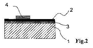
A method for the selective doping of silicon of a silicon substrate (1) for
producing a pn-junction in the silicon is
characterized by the following steps: a) Providing the surface of the silicon
substrate (1) with a doping agent (2) based on phosphorous,
b) heating the silicon substrate (1) for creating a phosphorous silicate glass
(2) on the surface of the silicon, wherein
phosphorous diffuses into the silicon as a first doping (3), c) applying a
mask (4) on the phosphorous silicate glass (2), covering
the regions (5) that are later highly doped, d) removing the phosphorous
silicate glass (2) in the non-masked regions, e) removing
the mask (4) from the phosphorous silicate glass (2), f) again heating for the
further diffusion of phosphorous from the phospho-rous
silicate glass (2) into the silicon as a second doping for creating the highly
doped regions (5), g) complete removal of the
phosphorous silicate glass (2) from the silicon.
Un procédé de dopage sélectif du silicium d'un substrat de silicium (1), pour la production d'une jonction pn dans le silicium, est caractérisé par les étapes suivantes : a) application à la surface du substrat de silicium (1) d'un dopant à base de phosphore (2), b) ensuite chauffage du substrat de silicium (1) afin de produire un verre de silicate de phosphore (2) à la surface du silicium, le phosphore se diffusant simultanément dans le silicium pour constituer un premier dopage (3), c) application sur le verre de silicate de phosphore (2) d'un masque (4) qui recouvre les zones (5) qui seront fortement dopées, d) élimination du verre de silicate de phosphore (2) dans les zones non masquées, e) élimination du masque (4) de la couche de verre de silicate de phosphore (2), f) nouveau chauffage pour poursuivre la diffusion de phosphore provenant du verre de silicate de phosphore (2) dans le silicium, pour constituer le second dopage produisant les zones fortement dopées (5), g) élimination totale du verre de silicate de phosphore (2) sur le silicium.
Note: Claims are shown in the official language in which they were submitted.
Note: Descriptions are shown in the official language in which they were submitted.
2024-08-01:As part of the Next Generation Patents (NGP) transition, the Canadian Patents Database (CPD) now contains a more detailed Event History, which replicates the Event Log of our new back-office solution.
Please note that "Inactive:" events refers to events no longer in use in our new back-office solution.
For a clearer understanding of the status of the application/patent presented on this page, the site Disclaimer , as well as the definitions for Patent , Event History , Maintenance Fee and Payment History should be consulted.
| Description | Date |
|---|---|
| Inactive: IPC assigned | 2015-12-14 |
| Inactive: IPC assigned | 2015-12-14 |
| Inactive: First IPC assigned | 2015-12-14 |
| Inactive: IPC removed | 2015-12-14 |
| Inactive: IPC removed | 2015-12-14 |
| Inactive: IPC assigned | 2015-12-14 |
| Inactive: IPC assigned | 2015-12-14 |
| Application Not Reinstated by Deadline | 2014-04-09 |
| Time Limit for Reversal Expired | 2014-04-09 |
| Inactive: IPC expired | 2014-01-01 |
| Inactive: IPC removed | 2013-12-31 |
| Deemed Abandoned - Failure to Respond to Maintenance Fee Notice | 2013-04-09 |
| Inactive: IPC expired | 2012-01-01 |
| Inactive: IPC removed | 2011-12-31 |
| Inactive: Cover page published | 2011-01-13 |
| Inactive: IPC assigned | 2010-12-06 |
| Inactive: IPC assigned | 2010-12-06 |
| Inactive: IPC assigned | 2010-12-06 |
| Application Received - PCT | 2010-12-06 |
| Inactive: First IPC assigned | 2010-12-06 |
| Inactive: Notice - National entry - No RFE | 2010-12-06 |
| Inactive: IPC assigned | 2010-12-06 |
| National Entry Requirements Determined Compliant | 2010-10-13 |
| Application Published (Open to Public Inspection) | 2009-10-22 |
| Abandonment Date | Reason | Reinstatement Date |
|---|---|---|
| 2013-04-09 |
The last payment was received on 2012-03-30
Note : If the full payment has not been received on or before the date indicated, a further fee may be required which may be one of the following
Please refer to the CIPO Patent Fees web page to see all current fee amounts.
| Fee Type | Anniversary Year | Due Date | Paid Date |
|---|---|---|---|
| Basic national fee - standard | 2010-10-13 | ||
| MF (application, 2nd anniv.) - standard | 02 | 2011-04-11 | 2010-10-13 |
| MF (application, 3rd anniv.) - standard | 03 | 2012-04-10 | 2012-03-30 |
Note: Records showing the ownership history in alphabetical order.
| Current Owners on Record |
|---|
| GEBR. SCHMID GMBH & CO. |
| Past Owners on Record |
|---|
| DIRK HABERMANN |

