Note : Les descriptions sont présentées dans la langue officielle dans laquelle elles ont été soumises.
CA 02721298 2010-10-13
P 48275 WO 1 PCT/EP2009/002671
Method for the selective doping of silicon and silicon
substrate treated therewith
Fields of application and Prior Art
The invention relates to a method for the selective
doping of silicon of a silicon substrate in order to
produce a pn junction in the silicon. This method is
required for example in the production of solar cells.
The selective doping of the emitter of silicon for the
production of a pn junction in silicon is used to
improve the contact-making and conduction properties in
solar technology. The efficiency of solar cells can be
increased by means of this process. Laser technologies
wherein the doping medium diffuses into the silicon by
means of a high-energy laser beam have previously been
used for the production of selective emitters. Other
methods are based on the plasma etching of highly doped
emitters. The regions in which the high doping is
intended to be retained are masked beforehand.
One example of further methods is US 5,871,591, wherein
in principle the regions in which the initially high
doping is intended to be retained after etching are
usually masked lithographically. These methods
therefore remove a thin layer, usually 100-200 nm
thick, having a high doping near the surface, in order
to obtain a selective emitter distribution. One
disadvantage of these methods, however, is that the
etching of the surface has to be effected very
precisely in order not to bring about a significant
loss in the efficiency of the solar cells. In the case
of laser-aided technologies, there is likewise the risk
of severe damage to the solar cell surface, which is
why this technology is also used only very occasionally
in solar technology.
CA 02721298 2010-10-13
P 48275 WO 2 PCT/EP2009/002671
Object and way of achieving it
The invention is based on the object of providing an
initially mentioned method as well as a silicon
substrate treated therewith whereby problems in the
prior art can be eliminated and, in particular, an
efficient and readily practicable method for the
selective doping of a silicon substrate can be
achieved.
This object is achieved by means of a method comprising
the features of Claim 1 as well as a silicon substrate
comprising the features of Claim 7. Advantageous and
preferred configurations of the invention are specified
in the further claims and are explained in more detail
below. In this case, some of the features are mentioned
only for the method or the silicon substrate, but are
intended to be applicable independently thereof to all
aspects of the invention. The wording of the claims is
incorporated by express reference in the content of the
description. Furthermore, the wording of the priority
application DE 102008019402.6 of 14 April 2008 in the
name of the present applicant is incorporated by
express reference in the content of the present
description.
The method has the following steps according to the
invention. In a step a), the surface of the silicon or
of the silicon substrate is coated with a dopant which
is based on phosphorus or contains phosphorus. By way
of example, this is a solution composed of phosphoric
acid. In a step b) afterwards, the silicon substrate is
heated, as is the dopant, in order to produce
phosphosilicate glass from the dopant on the surface.
In this case, phosphorus is simultaneously diffused
into the silicon as first doping of the silicon
CA 02721298 2010-10-13
P 48275 WO 3 PCT/EP2009/002671
substrate. The intensity of this doping can be set by
the duration and temperature of the heating.
In a subsequent step c), a masking is applied to the
phosphosilicate glass on the surface of the silicon
substrate. In this case, the masking is applied in such
a way that it covers the subsequently highly doped
regions of the silicon substrate. In a subsequent step
d), the phosphosilicate glass is removed in the
non-masked regions. Afterwards in turn, in a step e),
the masking is removed from the surface or the
phosphosilicate glass. In a subsequent step f), the
silicon substrate is heated anew in order to bring
about a further indiffusion of phosphorus from the
residual phosphosilicate glass into the silicon. This
is the second doping of the silicon substrate in order
to produce the highly doped regions. In the regions
that are free of phosphosilicate glass, only the
comparatively low phosphorus doping near the surface
serves as a secondary doping source for the deeper
diffusion of phosphorus into the base material. In a
further step g), the remaining phosphosilicate glass
and the oxide on the weakly doped regions are also
completely removed from the silicon substrate. This
procedure not only generally provides a selective
doping of a silicon substrate with highly doped regions
that can form emitters of a solar cell. It is primarily
also possible to provide a method which provides
suitable production or processing of silicon substrates
on a large scale. The method can primarily be carried
out in a continuous-throughput apparatus. Complicated
technology such as lasers or plasma etching sources can
be obviated.
In a further configuration of the method according to
the invention, the phosphorus-based dopant can be a
solution containing phosphoric acid.
CA 02721298 2010-10-13
P 48275 WO 4 PCT/EP2009/002671
A printing technology can be used to apply the masking
to the silicon substrate and the phosphosilicate glass
formed thereon. This can be effected either by means of
screen printing or alternatively by means of so-called
inkjet printing technology. In this case, the masking,
which comprises a wax or resist, for example, is
applied in liquid or pasty form by means of a method
corresponding to that used in so-called inkjet
printers. A desired masking can thereby be produced
both very accurately and rapidly and over a large area.
By means of this method, a contact grid can be produced
for example as a highly doped or conductive emitter,
wherein the solar cell is formed by the silicon
substrate. The highly doped regions arise as a result
of the double doping of the silicon. The doping can be
effected even more intensely primarily in step f) of
the second doping by means of a longer duration of
action or longer heating. Consequently, the doping can
be many times higher in the highly doped region than in
the other, more lightly doped regions.
In order to remove the phosphosilicate glass in the
non-masked regions in accordance with step c), an
etching process can be used. By way of example,
HF-based etching solutions are appropriate here, but
other etching media are also possible. This can be
effected either in one process step or in a plurality
of steps with different chemicals.
A continuous-throughput apparatus for carrying out the
method can comprise a plurality of modules. In this
case, a plurality of the steps can possibly also be
carried out in one module. A horizontal
continuous-throughput apparatus on which the silicon
substrates are conveyed and treated in a horizontal
position is particularly preferred.
CA 02721298 2010-10-13
P 48275 WO 5 PCT/EP2009/002671
These and further features emerge not only from the
claims but also from the description and the drawings,
wherein the individual features can be realized in each
case by themselves or as a plurality in the form of
subcombinations in an embodiment of the invention and
in other fields and can constitute advantageous and
inherently protectable embodiments for which protection
is claimed here. The subdivision of the application
into sub-headings and individual sections does not
restrict the general validity of statements made
hereunder.
Brief description of the drawings
An exemplary embodiment of the invention is
schematically illustrated in the drawings and is
explained in more detail below. In the drawings,
figures 1 to 6 show method steps a) to g) on a silicon
substrate for the production of a solar cell.
Detailed description of the exemplary embodiment
Figure 1 illustrates a silicon substrate 1, to which a
dopant has been applied over a large area in accordance
with step a) and step b). This dopant 2 contains
phosphorus or is based on phosphorus and is for example
a solution composed of phosphoric acid. Furthermore,
phosphorus is indiffused from the dopant 2 into the
silicon substrate 1 or the top side thereof by heating
in a manner not illustrated in greater detail, for
example by radiant heaters or the like. A lightly doped
region 3 has arisen as a result, which is illustrated
by the cross hatching.
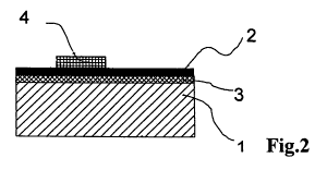
Figure 2 illustrates how a masking 4 is applied to the
top side of the dopant 2 in accordance with step c).
This masking 4 is applied by means of an inkjet
printing technology in the manner described above and
CA 02721298 2010-10-13
P 48275 WO 6 PCT/EP2009/002671
advantageously runs largely in the narrow tracks
illustrated, though other masking patterns are also
possible. These tracks of the masking 4 correspond to
the desired highly doped regions, which will be
discussed in even more detail below.
Figure 3 illustrates how, in accordance with step d),
the dopant 2, which has been converted into
phosphosilicate glass after the heating in accordance
with figure 1 and step b), has been removed wherever it
is not covered by the masking 4. Consequently,
essentially the surface of the lightly doped region 3
of the silicon substrate 1 is uncovered.
Correspondingly formed regions of the phosphosilicate
glass 2 are still present beneath the masking 4.
As is illustrated in Figure 4, the masking 4 is
subsequently removed in accordance with step e). While
the phosphosilicate glass can be removed by HF etching
in step d) in accordance with figure 3, a much less
aggressive solution suffices for removing the masking
4.
Figure 5 illustrates how, in accordance with step f),
phosphorus indiffuses anew into the silicon substrate 1
by renewed heating from the now uncovered
phosphosilicate glass 2 with a form corresponding to
the masking 4 that was applied and removed again. The
phosphorus from the phosphosilicate glass 2 forms a
narrow region with a form corresponding to the
phosphosilicate glass 2 in accordance with figure 4 or
the masking 4 in accordance with figure 2. It is also
the case moreover that in the lightly doped region 3 of
the silicon substrate 1, that is to say essentially
over the whole area, phosphorus is diffused from the
region near the surface into the silicon substrate 1
somewhat more deeply than is the case after the first
diffusion step. In the lightly doped region 3 and in
CA 02721298 2010-10-13
P 48275 WO 7 PCT/EP2009/002671
the highly doped region 5, the phosphorus concentration
decreases from the surface into the base material,
wherein the doping depth can indeed differ.
In accordance with step g), as is illustrated in figure
6, the remaining phosphosilicate glass 2 is also
removed, advantageously again by HF etching. A thin
layer with an oxide in the weakly doped region is
likewise removed during this step. The silicon
substrate 1 in accordance with figure 6 is then present
with a region 3 lightly doped over the whole area. The
highly doped regions 5 run in this lightly doped region
3 and form the low-impedance emitter or a so-called
contact grid in a solar cell.
The invention enables a selective doping of a silicon
substrate to be effected by means of methods which are
readily controllable technologically and which can all
be carried out in continuous fashion. It is thus
possible by way of example, as described, to produce a
contact grid for a solar cell.