Note: Descriptions are shown in the official language in which they were submitted.
CA 02721393 2014-01-07
WO 2009/149069
PCT/US2009/045950
Conductive Coating of Implants with Inductive Link
Field of the Invention
100021 The present invention relates to medical implants, and more
specifically to a
surface coating for such devices.
Background Art
100031 Some implantable devices such as Cochlear Implants (CI's) transfer
electrical
energy and data via an inductive link through the skin. This requires that the
implanted
receiving coils are not electrically shielded, which would interfere with the
signal transfer.
For that reason, implant coils are either encapsulated by a non-metallic
housing (e.g. made
of ceramics) or are embedded into silicone outside the hermetic encapsulation
of the
electronic circuit.
10004] Just as with any surgical procedure, there is also some risk during
implant surgery
of postoperative infections at the surgical site. This risk is generally small
and depends on
several factors including hygiene standards in the operating room and surgical
technique.
One technical solution to further reduce the risk of bio-film growth and
infection at the
implant device is an antibiotic coating. One specific example would be a
silver-based
coating since silver ions are antibiotic (even against drug-resistant
bacteria) and also
prevent fungal decay around the implanted device. Depending on several factors
(such as
the silver concentration) a problem may arise in that silver coating over the
inductive coil
may cause some electrical shielding of the inductive link, thereby negatively
affecting
both power transfer to the implant device and also data communication in both
directions.
The inductive link may be influenced even if there is a high DC resistance of
the
conductive coating.
[00051 Implant devices also may have an internal magnet in the center of the
implanted
-1-
= CA 02721393 2014-01-07
WO 2009/149069
PCT/US2009/045950
coil for providing an attractive magnetic force to a corresponding external
magnet in the
external coil. In some designs the internal magnet may be removable such as
for magnetic
resonance imaging (MRI) in order to avoid interactions between the internal
magnet and
the external MRI magnetic fields the attendant potential risks such as torque
on the
implant device, imaging artifacts and weakening of the internal magnet. A
typical
procedure is a first surgery to remove the internal magnet or to replace the
magnet by a
non-metallic space holder prior to MRI scanning, and then after the MRI
scanning, a
second surgery to replace the internal magnet.
[00061 Depending on the design of the removable magnet, there may be some dead
space
between thc internal magnet and the surrounding part of the implant (e.g. a
silicone
material containing the implant coil). Such a dead space can potentially raise
a risk of bio-
film formation and associated infection which is difficult to treat.
[0007i Currently, various ways to avoid some of these problems include:
= No conductive coating in the area of the inductive coil
= Keep the conductive coating at a low level where the inductive link is
not
negatively affected
= For the internal magnet, to have no removable magnet or have a design
(geometry)
which keeps the dead space very small.
Summary of the Invention
100081 Embodiments of the present invention are direct to an implantable
device that
includes an implanted coil for receiving a transcutaneous coil signal from an
external
transmitting coil. A coil housing contains the coil and has a non-conductive
surface. A
conductive coating covers at least a portion of the housing surface and forms
a non-
shielding pattern that minimizes interaction with the coil signal.
[0009] In further specific embodiments, the non-shielding pattern may
form a web, mesh, and/or radial line pattern. The conductive coating may be an
antibiotic
coating and/or a silver-based coating.
-2-
CA 02721393 2010-10-13
WO 2009/149069
PCT/US2009/045950
[0010] The coil housing may be formed of a ceramic material and may also
contain a
signal processing module for processing the received coil signal. Embodiments
may also
have an electrode lead connected to the coil housing, wherein the conductive
coating
pattern further covers at least a portion of the electrode lead. The
implantable device may
be an element in a cochlear implant system.
[0011] Embodiments of the present invention also include an implantable device
including
an implanted magnet that interacts with an external magnet to maintain the
external
magnet in a constant position adjacent to the implanted magnet. A magnet
housing
contains the magnet. A therapeutic coating is between at least a portion of
the magnet and
the magnet housing for delivery of a therapeutic benefit in the vicinity of
the therapeutic
coating.
[0012] In further such embodiments, the therapeutic coating may specifically
be an
antibiotic coating and the therapeutic benefit may include an antibiotic
effect. The
therapeutic coating may be a silver-based coating and/or a colloidal-based
coating, and the
therapeutic benefit may include preventing formation of a bio-film in the
vicinity of the
therapeutic coating.
[0013] The implanted magnet may be a removable magnet. The magnet housing may
be
formed of a ceramic material and/or may further contain an implanted coil for
receiving a
transcutaneous coil signal from an external transmitting coil. The magnet
housing also
may include a signal processing module for processing the received coil
signal. The
implantable device may be an element in a cochlear implant system.
[0014] Embodiments of the present invention also include an implantable device
having
an implanted coil for receiving a transcutaneous coil signal from an external
transmitting
coil. A coil housing contains the implanted coil which is embedded in a non-
shielding
pattern of conductive containment material divided by non-conductive
separating
structures, and the pattern minimizes interaction of the containment material
with the coil
signal.
-3-
CA 02721393 2010-10-13
WO 2009/149069
PCT/US2009/045950
[0015] In specific such embodiments, the non-shielding pattern may form a web,
mesh, or
radial line pattern. The containment material may include an antibiotic
component and/or a
silver-based component and/or a colloidal-based component. The coil housing
may be
formed of a ceramic material and/or may also contain a signal processing
module for
processing the received coil signal. The implantable device may be an element
in a
cochlear implant system.
Brief Description of the Drawings
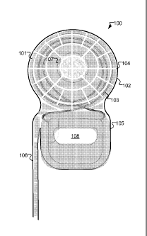
[0016] Figure 1 shows an implantable device having a patterned conductive
coating
according to an embodiment of the present invention.
[0017] Figure 2 shows another type of implantable device having a patterned
conductive
coating according to another embodiment of the present invention.
[0018] Figure 3 shows an implantable device having inductive link coils
embedded in a
low conductivity structure according to an embodiment of the present
invention.
[0019] Figure 4 A-B shows an implantable device having a removable magnet and
using a
therapeutic coating according to an embodiment of the present invention.
[0020] Figure 5 A-B shows another implantable device having a removable magnet
and
using a therapeutic coating according to another embodiment of the present
invention.
Detailed Description of Specific Embodiments
[0021] Embodiments of the present invention are directed to an implantable
device that
uses a surface coating and/or bulk material which are developed in a pattern
that avoids
many of the problems that arise in previous approaches. Some of the benefits
which
specific embodiments of a therapeutic surface coating may provide include,
without
limitation:
= unimpeded data and energy transfer through the inductively coupled
transcutaneous link
= avoidance of RF-heating of the surface coating due to eddy currents (e.g.
in the
-4-
CA 02721393 2010-10-13
WO 2009/149069
PCT/US2009/045950
event of Magnetic Resonance Imaging (MRI) or even during normal use).
o This may be especially important during the charging phase of an
implanted battery when a relatively high amount of RF power is sent over
the inductive link.
= good back-telemetry data transfer properties.
[0022] Figure 1 shows an implantable device 100 having a patterned conductive
coating
101 according to an embodiment of the present invention. The upper circular
portion is a
coil housing 102 containing an implanted coil 103 for receiving a
transcutaneous coil
signal from an external transmitting coil. The coil housing 102 also contains
an internal
magnet 107 for maintaining an external magnet of an external transmitting coil
in a
constant position adjacent to the implanted magnet 107.
[0023] The coil housing 102 has a non-conductive outer surface 104, at least a
portion of
which is covered by the conductive coating 101 which forms a non-shielding
pattern that
minimizes interaction with the coil signal. The conductive coating 101 does
not
homogeneously cover the complete surface area of the coil housing 102, but
rather is
separated into smaller individual areas so that the negative influence on the
inductive link
is kept as small as possible, while at the same time, the area which is not
coated shall be
kept as small as possible so as to maximize the therapeutic benefits of the
coating. For
example, the non-shielding pattern of the conductive coating 101 may form a
radial line
pattern as shown in Fig. 1, or alternatively some other pattern such as a web
or a mesh
pattern (as in Fig. 2). The conductive coating 101 may be an antibiotic
coating and/or a
silver-based coating and/or a colloidal-based coating. Some embodiments may be
limited
by production processes and material properties (e.g. minimum effective
thickness of non-
conductive fragmentation lines) and efficacy of the conductive coating 101.
The relative
amount percentage of the surface of the coil housing 102 (and the dimension of
areas) not
covered by the conductive coating 101 and/or the size of the non-conductive
fragmentation paths should be minimized to preserve good therapeutic
properties. There
may be further benefits to the use of a conductive coating 101 beyond the
therapeutic
antibiotic effect mentioned. For example:
= to increase mechanical impact protection of the implantable device 100
-5-
CA 02721393 2010-10-13
WO 2009/149069
PCT/US2009/045950
= to shield the implantable device 100 from ionizing radiation
It may further be useful to pattern the conductive coating 101 as discussed
above for such
considerations.
[0024] The implantable device 100 may also contain a signal processing module
105 for
processing the received coil signal. For example, in a cochlear implant
system, the signal
processing module 105 contains circuitry for developing electrode stimulation
signals
which are output through an attached electrode lead 106, the other end of
which applies
the stimulation signals to target nervous tissue. The conductive coating 101
may also
cover some or all of the signal processing module 105 and/or the electrode
lead 106 with
or without the pattern used over the coil housing 102. For example, with a
relatively long
electrode lead 106 there may be a risk of RF-induced heating of the conductive
coating
101, which can be mitigated by using a non-shielding (i.e. discontinuous or
partitioned)
pattern. There may be no conductive coating 101 over some elements of the
implantable
device 100 such as, for example, electrode ground contact 108.
[0025] Figure 2 shows an example of another type of implantable device 200
having a
mesh-patterned conductive coating 201 according to another embodiment of the
present
invention. In this embodiment, a single implant housing 202 made of a non-
conductive
ceramic material which contains the implanted coil 203 as well as the internal
magnet and
signal processing module (not shown). In this embodiment, the conductive
coating 201
covers the entire implantable device 200 with the pattern extending over the
implanted coil
203 and the electrode lead 206, with the remainder of the coating being
unpatterned.
[0026] Figure 3 shows a cross-sectional view of an implantable device 300
similar to the
two-part device in Fig. 1, having a coil housing 302 and a separate signal
processing
module 305. Within the coil housing 302 are inductive link coils 303 for
receiving a
transcutaneous coil signal from an external transmitting coil. The coil
housing 302 also
contains an implanted magnet 307 that interacts with an external magnet to
maintain the
external magnet in a constant position adjacent to the implanted magnet.
[0027] The inductive link coils 303 are embedded in a low conductivity
structure arranged
-6-
CA 02721393 2010-10-13
WO 2009/149069
PCT/US2009/045950
in a non-shielding pattern of conductive containment material 308 (e.g.,
silicone
impregnated with conductive material) which is divided by non-conductive
separating
structures 309, where the pattern minimizes interaction of the containment
material 308
with the coil signal. In specific such embodiments, the non-shielding pattern
may form a
web, mesh, or radial line pattern. In the embodiment shown in Fig. 3, the non-
conductive
separating structures 309 separate individual link coils 303 from each other
to minimize
the shielding effect of the surrounding conductive containment material 308.
The
containment material 308 may include an antibiotic component and/or a silver-
based
component. It may be beneficial to implement non-conductive fragmentations
need across
the complete cross-section of the inductive link coils 303.
[0028] Figure 4 A-B shows an implantable device 400 having a removable
internal magnet
407 and using a therapeutic coating according to an embodiment of the present
invention.
The cylindrical internal magnet 407 is contained in a corresponding
cylindrical magnet
housing 402 and interacts with an external magnet to maintain the external
magnet in a
constant position adjacent to the implanted magnet 407. In one specific
embodiment, the
magnet housing 402 is in the form of a pocket of soft silicone material having
an opening
at the top through which the internal magnet 407 may be surgically removed
when needed.
[0029] A therapeutic coating 401 covers the external surface of the implanted
magnet 407
and the corresponding surfaces of the magnet housing 402 which engage the
internal
magnet 407. The therapeutic coating 401 provides of a therapeutic benefit such
as
preventing formation of a bio-film in the vicinity of the therapeutic coating,
thereby
avoiding infection. Specifically, the therapeutic coating 401 may include
antibiotic coating
and/or a silver-based coating. It may also be useful to provide a therapeutic
coating 401 on
any dummy parts (e.g., a non-metallic space holder replacing the internal
magnet 407
during an MRI) and/or replacement magnets (inserted after the MRI).
[0030] As with the conductive coatings discussed above, the therapeutic
coating 401 may
also be arranged in a non-uniform pattern. Figure 5 A-B shows another
implantable device
500 having a different shaped non-cylindrical removable internal magnet 507
and using a
therapeutic coating 501 according to another embodiment of the present
invention. In
-7-
CA 02721393 2010-10-13
WO 2009/149069
PCT/US2009/045950
some specific embodiments, it may also be useful to physically seal the dead
space
between the magnet and the magnet housing and/or provide a tight fit between
them that
prevents micro-movements of the magnet relative to the magnet housing when the
external
coil is removed or placed over the implant, in order to further reduce the
risk of bio-film
growth in the magnet area.
[0031] Although various exemplary embodiments of the invention have been
disclosed, it
should be apparent to those skilled in the art that various changes and
modifications can be
made which will achieve some of the advantages of the invention without
departing from
the true scope of the invention.
-8-