Note: Descriptions are shown in the official language in which they were submitted.
CA 02721512 2010-10-15
-1-
DESCRIPTION
[Title of the Invention]
Circuit Protection Device
[Field of the Invention]
[0001]
This invention relates to a circuit protection device (or
a circuit protection element); more specifically, it relates to
a circuit protection device comprising a circuit switching
element comprising a bimetal element and a movable
terminal, and a PTC element, as well as to an electrical
circuit (or an electrical apparatus) having such a protection
device. Such a circuit protection device may be used as a
protection element in electrical circuits using various high
voltage (preferably 12 V or larger, for example 24 V or
higher) or high current (preferably 15 A or higher, for
example 30 A or larger) batteries, which are, for example,
used in electric cars, cordless cleaners, power tools,
wireless base stations, and the like. It is noted that the
above mentioned voltage and current are normal voltage
and current when an electric device (various electric
devices including a battery) which uses the circuit
protection device according to the present invention works
without a problem.
CA 02721512 2010-10-15
-2-
[Background Art]
[0002]
In various electrical circuits, a circuit protection
device is incorporated into its circuit in order to protect
electrical/electronic devices and/or electrical/electronic
components incorporated in the circuit when a voltage
which is larger than the rated voltage is applied to the
circuit and/or when a current which is larger than the rated
current through the circuit.
[0003]
For such a circuit protection device, the use of a
bimetal element as a circuit switching element and a PTC
element connected in parallel has been proposed (see the
patent reference below). In such a circuit protection device,
substantially all of the current flowing through the circuit
under normal operating conditions (i.e. under conditions of
a voltage equal to or below the rated voltage and a current
equal to or below the rated current) flows between the
contacts of the circuit switching element, which are in
contact with each other. Under
conditions of an
overcurrent, for example, the bimetal element of the circuit
switching element rises in temperature and is actuated, and
its contact is separated from the corresponding stationary
contact and opened, so that the current is diverted to the
CA 02721512 2010-10-15
-3-
PTC element. As a result, the PTC element trips into a
high temperature, high resistance state through the
overcurrent, substantially cutting off the current flowing
through the PTC element. At this point, the high
temperature of the PTC element maintains the bimetal part
at high temperature, thereby maintaining the open state of
the circuit switching element. In other words, the latched
state of the circuit switching element is maintained. It is
said that, in such a circuit protection device, there is no
need to switch the current and therefore there is no arcing
at the contacts of the circuit switching device.
[Prior Patent Reference]
[0004]
Patent Reference 1:
Japanese Patent Kohyo Publication No. 1999-512598
[Disclosure of the Invention]
[Problems to be Solved by the Invention]
[0005]
The inventor studied the abovementioned. circuit
protection device, as a result of which it has been noticed
that, in a circuit protection device wherein the PTC element
is merely connected in parallel relative to the circuit
switching element, when the circuit switching element is
CA 02721512 2010-10-15
-4-
actuated and the contacts of the bimetal element are
separated from its corresponding stationary contacts,
arcing occurs at the contacts of the circuit switching
element, and in the worst case, may cause the contacts to
weld and form a welded area. When such a welded area is
formed, the circuit protection device will not function and
will not be able to protect the electrical/electronic devices
and/or the electrical/electronic components incorporated in
the circuit. Therefore, the problem that the present
invention aims to solve is to provide the abovementioned
circuit protection device with an even more improved
possibility of protecting the circuit. In other
words, when
instantaneously shutting off current flowing between the
contacts, there is a problem in that a welded area is formed
between these contacts.
[Means to Solve the Problems]
[0006]
The present invention provides a circuit protection
device which comprises a circuit switching element
comprising a bimetal element as a circuit switching
component and a movable terminal as well as a PTC
element, the circuit protection device being characterized
by:
(1) the PTC element and the movable terminal being
CA 02721512 2016-02-24
-5-
connected electrically in parallel;
(2) the circuit switching element being able to cut off
current which flows through the circuit switching element by
moving, through actuation of the bimetal element at its
actuating temperature (Top), the movable terminal
positioned to pass the current, and being able to pass
current through the circuit switching element by moving,
through resetting of the bimetal element at its reset
temperature (Tcl), the movable terminal positioned to pass
current;
(3) the actuating temperature (Top) of the bimetal
element being at least 20 *C higher than the reset
temperature (Tcl) of the bimetal element;
(4) a trip temperature (Ttr) of the PTC element being
at least 10 C higher than the actuating temperature of the
bimetal element; and
(5) the bimetal element being placed between the PTC
element and the movable terminal. The PTC element is a polymer element.
The present invention also provides an electrical circuit comprising such a
circuit protection device, and further provides an electrical apparatus
comprising such an electrical circuit.
[Effect of the invention]
[0007]
When a circuit protection device of the present
CA 02721512 2010-10-15
-6-
invention is incorporated in an electric circuit, the
formation of a welded area between contacts on the
movable terminal (also called movable contacts) and their
corresponding contacts on the stationary terminal may be
further suppressed. As a result, the circuit protection
function of the circuit protection device is further improved.
[Brief Explanation of the Drawings]
[0 00 8]
[Figure 1] Figure 1 shows schematically an electrical
circuit of an electrical apparatus incorporating the circuit
protection device of the present invention.
[Figure 2] Figure 2 shows a schematic cross-section of
one embodiment of the circuit protection device of the
present invention.
[Figure 3] Figure 3 shows schematically an exploded
perspective view of the circuit protection device in Figure 2.
[Figure 4] Figure 4 shows a schematic cross-section of
one embodiment of the circuit protection device of the
present invention.
[Figure 5] Figure 5 shows a temperature vs. resistance
curve for the circuit protection device of the present
invention.
[Figure 6] Figure 6 shows the change in time vs.
current/voltage in smoothed out lines when DC30V/50A is
CA 02721512 2010-10-15
-7-
applied to an electrical circuit incorporating the circuit
protection device of the present invention.
[Figure 7] Figure 7 shows the change in time vs.
current/voltage in smoothed out lines when DC30V/100A is
applied to an electrical circuit incorporating the circuit
protection device of the present invention.
[Explanation of the References]
[0009]
1 ¨ circuit protection device; 3 ¨ electrical circuit;
5 ¨ electrical component; 7 ¨ power source;
10 ¨ PTC element; 12 ¨ circuit switching element;
14 ¨ bimetal element; 16 ¨ movable terminal;
18, 19 ¨ contact; 20, 21 ¨ stationary terminal;
22, 23 ¨ contact; 30 ¨ lower side lead;
32 ¨ upper side lead; 38 ¨ base plate;40 ¨ spacer;
42¨ upper plate; 44 ¨ pin; 46¨ casing; 48¨ opening;
50 ¨ insulating material; 52 ¨ adhesive.
[Embodiments to Carry Out the Invention]
[0010]
As a result of studying the problem of the welded area
being formed at the contacts of the circuit switching
element, in the circuit protection device comprising the PTC
element and the circuit switching element, when adopting a
CA 02721512 2010-10-15
-8-
arrangement using a bimetal element as the circuit
switching component whereby the current flowing through
the circuit switching element is cut off/turned on by the
actuation of the bimetal element (in other words, actuation
and reset as described below) to move the movable
terminal,
it has been found to be desirable regarding the
abovementioned problem of the welded area being formed
that a circuit switching element comprising a bimetal
element and a movable terminal is used which is configured
to cut off the current flowing through the circuit switching
element by means of the bimetal element actuating (from
the reset state) and turn on the current flowing through the
circuit switching element by means of the bimetal element
resetting (from the actuated state); and
that when placing the bimetal element between the
PTC element and the movable terminal,
(a) the actuating temperature (Top) of the bimetal
element is at least 20 C higher than its reset temperature
(Tel), and
(b) the trip temperature (Ttr) of the PTC element is at.
least 10 C higher than the actuating temperature of the
bimetal element.
[0011]
When the temperature of a bimetal element rises to or
CA 02721512 2010-10-15
-9-
above a certain temperature or above, the shape of the
bimetal element changes to a different shape through the
actuation of the bimetal element. The temperature at which
it actuates is called the actuating temperature (Top).
During such actuation, the action of the movable contacts
of the movable terminal in a current carrying state moving
away from the corresponding stationary contacts of the
stationary terminal and separating these contacts from each
other is macroscopically an instantaneous action. When
this action is seen microscopically, it can be considered as
a gradually separating action in the continuous and
extremely short time in which the contacts separate. At the
beginning of this extremely short time, the rated current
flows between the contacts, and at the end of this
extremely short time the current is shut off between the
contacts. In other words, at the beginning of this extremely
short time, the resistance between the contacts is
substantially zero, and at the end of this extremely short
time, the resistance is increased infinitely.
[00 1 2]
Therefore, when the PTC element has already tripped
and is in a high-resistance state before the contacts are
separated, the current that had been flowing between the
contacts is not diverted smoothly to the PTC element.
Taking this into consideration, it is desirable for the PTC
CA 02721512 2010-10-15
-10-
element to have a sufficiently low resistance when the
bimetal is actuated and the movable contacts of the
movable terminal separate from their corresponding
contacts. The trip temperature (Ttr) of the PTC element
needs to be higher than the actuating temperature (Top) of
the bimetal element; as a result of the inventors'
experience and experimental studies, it has been found that
at least 30 C higher is preferred, at least 20 C higher is
more preferred, and at least 10 C higher is particularly
preferred.
[0013]
The PTC element becomes highly resistant quickly after the
actuation of the bimetal when the temperature difference
between Ttr and Top is appropriately large, so that
overcurrents can be cut off immediately. Taking this into
consideration, it has been thought that the abovementioned
temperature differences are appropriate. In this case,
when a polymer PTC element as described below is used as
the PTC element, its initial resistance (i.e. the resistance in
the state before tripping) is considerably smaller, for
example roughly 1/100 compared with a ceramic PTC
element, so from this point, the use of a PTC element is
particularly preferred.
[0014]
Further, when the temperature difference (ATI)
CA 02721512 2010-10-15
=
- 1 1 -
between Ttr and Top is excessively large, the duration of
the overcurrent flowing through the PTC element becomes
long, and in some cases this may not necessarily be
desirable from the standpoint of the circuit protection.
Taking this into consideration, the temperature difference
between the trip temperature (Ttr) of the PTC element and
the actuating temperature (Top) of the bimetal element is
preferably 70 C or less, more preferably 50 C or less, and
particularly preferably 40 C or less. Therefore, the range
of AT1 is, for example, preferably 10 C5 LT 1 5 70 C, more
preferably 10 C5 AT1 550 C, and particularly preferably
10 C5 AT15 40 C.
[0015]
It is noted that the trip temperature of a PTC element
denotes the temperature at which the resistance of the PTC
element increases rapidly (for example 103 ¨ 106 times) in
the vicinity of a certain temperature when the temperature
of the PTC element is raised. With respect to this
temperature, information provided by the manufacturer or
seller (for example catalogs, specifications, etc.) may be
referred to for commercially available PTC elements. For
example, in catalogs of Tyco Electronics Raychem,
temperatures called actuating temperatures (typical values)
are listed as trip temperatures.
[0016]
CA 02721512 2010-10-15
-12-
Further, the view has been reached that, when the
PTC element became highly resistant and heated up, in
order to provide its heat to the bimetal element and
maintain the bimetal element in the actuated state, it is
desirable to place the bimetal element adjacently to the
PTC element with a gap in between (thus these elements
face to each other across the gap). Specifically, it has
been found that the bimetal element is preferably placed
between the PTC element and the movable terminal.
[0017]
In addition, the bimetal element in the actuated state
decreases in temperature, and when the temperature is
equal to or below a certain temperature, it reverts toward
its original shape, as a result of which the separated
contacts return to a contact state. This temperature is
called the reset temperature (Tcl). It has been seen that,
when this reset temperature is not very different from the
abovementioned actuating temperature, an overcurrent may
flow again in a state wherein the temperature has not
sufficiently decreased around the circuit protection device,
i.e. in a state wherein the abnormal condition occurring in
the circuit has not been resolved, so that the bimetal will
actuate again. As a result of further study, it has been
found that the actuating temperature (Top) of the bimetal
element is preferably at least 20 C higher than the reset
CA 02721512 2010-10-15
-13-
temperature (Tcl), and more preferably at least 30 C
higher. With respect to the actuating temperature and the
reset temperature for the commercially available bimetal
elements, information provided by the manufacturer (for
example catalog data, specification, etc.) may be referred
to.
[0018]
In the circuit protection device of the present
invention, the circuit switching element comprises a bimetal
element, as the circuit switching component as well as a
movable terminal. The bimetal element is a drive member
using a bimetal. In the circuit protection device of the
present invention, when current flowing in the movable
terminal (or if contacts are provided thereon, between these
contacts (i.e. movable contacts)) driven by the bimetal
element increases over a prescribed current and becomes
excessive, it changes from a certain shape (called a first
shape as described below) to another shape (called a
second shape as described below), as a result of which, the
movable terminal (or its contacts) in mutual contact
functions as a type of switch so structured as to separate
from the terminal with which it is in contact (for example
the contacts of the stationary terminal or its contacts (i.e.
stationary contacts)), or conversely to have separated
contacts come in mutual contact. Any known bimetal
CA 02721512 2010-10-15
-14-
element may be used for the bimetal element itself. It is
noted that such contact may be any one between the
terminals, between the contacts provided on the terminals
or between the terminal and the contacts.
[0019]
In such a bimetal element, the shape at the lower
temperature is called the first shape; when the temperature
of the element is increased from that state and the
temperature exceeds a certain temperature, the bimetal
element switches to a second shape. Also, when the
temperature of the bimetal element in the second shape is
decreased and the temperature goes below a certain
temperature, the bimetal element returns to the first shape.
Changing from the first shape to the second shape is called
"actuating" herein for convenience, and changing from the
second shape to the first shape is called "resetting" for
convenience. Such a change in shape is utilized to
separate the movable terminal (or the contacts provided
thereon), which has been in a contact state, from the
stationary terminal, or to have the movable terminal (or the
contacts provided thereon) come in contact with the
stationary terminals. In other words, the shape change of
the bimetal element is utilized as a driving force to change
the position of the movable terminal (or the contacts
provided thereon).
CA 02721512 2010-10-15
-15-
[0020]
The temperature at which the first shape changes to
the second shape is called "actuating temperature (Top)",
and the temperature at which the second shape changes to
the first shape is called "reset temperature (Top". Normally,
Top is higher than Tel. If the
reset temperature is
excessively close to the actuating temperature, this will
cause chattering, in which the switching of the contacts is
repeated when the equipment is in an abnormal state, so
that the circuit protection device will not function normally
in response to an overcurrent. In the circuit protection
device of the present invention, Top is at least 20 C higher
than Tcl, preferably at least 30 C higher, and more
preferably at least 40 C higher, for example 45 C higher.
[0021]
It is noted that if the reset temperature is excessively
low, the duration of period that the bimetal element causes
the circuit protection device to be latched becomes long,
which means that the time it takes for the circuit protection
element to return to its normal state takes longer, which in
some cases may not be desirable from the standpoint of
convenience in using the electrical equipment in which the
circuit protection element is incorporated. For example,
time may be required before an electrical equipment that
has stopped through an overcurrent caused by a high load
CA 02721512 2010-10-15
-16-
(for example a power drill) can be used again. Taking this
into consideration, the temperature difference (AT2)
between the actuating temperature (Top) and the reset
temperature (Tor) of the bimetal element is, for example,
preferably 60 C or lower, more preferably 55 C or lower,
and particularly preferably 50 C or lower. Thus, the range
of AT2 is, for example, preferably 20 C AT2 5 60
C,
more preferably 30 C AT2 5 55
C, and particularly
preferably 40 C 5 LI T2 s 50 C.
[0022]
For the movable terminal of the circuit switching
element as described above, one using platinum, gold,
silver, copper, carbon, nickel, tin, lead, and alloys thereof
(for example tin-lead alloy, silver-nickel alloy, etc.) as the
contact material may be mentioned as particularly desirable
for use in the circuit protection device of the present
invention. Among them, a movable terminal using silver or
a silver alloy (e.g. silver-nickel alloy or the like) as the
contact material is particularly preferred. It is of course
that the above explanation as to the movable terminal is
also applicable to the material which, forms the movable
contacts. It is noted that in the circuit protection device of
the present invention, the gap between the movable
terminal and the stationary terminal or the gap between the
movable contacts and the stationary contacts is preferably
CA 02721512 2010-10-15
-17-
relatively small, and it is preferably 0.5 ¨ 4 mm, particularly
2 mm or less, more preferably 0.7 ¨ 2 mm, particularly
preferably 0.8 - 1.5 mm, for example about 1 mm.
[0023]
In the circuit protection device of the present
invention, nickel, copper, manganese, iron, chrome, zinc,
molybdenum, and alloys thereof (for example nickel-copper,
nickel-iron and the like) for example may be mentioned as
particularly desirable for use in the bimetal element.
Among them, bimetal elements using nickel-copper-
manganese, nickel-iron, and the like, as the material
thereof are particularly preferred.
[0024]
In the circuit protection device of the present
invention, the PTC element connected in parallel to the
circuit switching element may be a conventional PTC
element that is itself used as a circuit protection device,
and its conductive element may be made of a ceramic or of
a polymer material. A particularly preferred PTC element is
one called a polymer PTC element, and a PTC element
comprising a conductive polymer element wherein
conductive fillers (for example carbon, nickel, nickel-cobalt
fillers) are dispersed in a polymer material (for example
polyethylene, polyvinylidene fluoride, etc.) may be suitably
used.
CA 02721512 2010-10-15
-18-
[0025]
When an electric device in which the circuit protection
device of the present invention is incorporated in a
prescribed circuit performs its intended function normally,
substantially all of the current flowing in the circuit passes
through the circuit switching element. Therefore, in the
circuit protection device of the present invention, the
resistance of the PTC element (resistance before tripping,
normally resistance at room temperature) has a resistance
value of at least 10 times the electrical resistance that the
movable terminal inherently has (or the resistance between
the contacts provided thereon; these resistance values are
normally 0.5 to 20 milliohms), preferably at least 50 times,
more preferably at least 100 times, and particularly
preferably at least 300 times.
[0026]
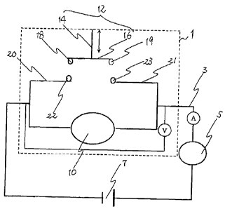
Figure 1 shows an electrical circuit 3 incorporating the
circuit protection devicel of the present invention
(enclosed in broken lines). The circuit 3 has a prescribed
electrical element (for example an electrical/electronic
device or component, etc.) 5, and the circuit protection
device 1 and a power source 7 are connected in series
thereto. The electrical element 5 is shown as a single
element, but this denotes a single electrical element or an
aggregate of a plurality of electrical elements included in
CA 02721512 2010-10-15
-19-
the circuit 3.
[0027]
The circuit protection device 1 of the present invention
comprises a PTC element 10 and a circuit switching
element 12. The circuit switching element 12 comprises a
bimetal element 14 and a movable terminal 16. The
movable terminal 16 has movable contacts 18 and 19 close
to its ends. The movable terminal 16 moves as shown by
the arrows through the actuation of the bimetal element 14
to come into contact with, or separate from, the stationary
contacts 22 and 23 provided on the facing stationary
terminals 20 and 21.
[0028]
In the illustrated embodiment, the contact 18 of the
movable terminal that had been in contact with the contact
22 of the stationary terminal 20 and the contact 19 of the
movable terminal that had been in contact with the contact
23 of the stationary terminal 21 are in a separated state
from the terminals 20 and 21 through the upward movement
of the movable terminal 16 due to the actuation based on
the temperature increase of the bimetal element. In this
state, all the current flowing through the circuit 3 flows
through the PTC element, as a result of which the PTC
element heats up, such heat maintaining the actuated state
of the bimetal element.
CA 02721512 2010-10-15
-20-
[0029]
Conversely, from the state shown in Figure 1, the
movable terminal moves through the temperature of the
bimetal element 14 decreasing and the bimetal resetting, so
that the contacts 18 and 22, and the contacts 19 and 23
come mutually in contact. In this state, substantially all the
current flowing through the circuit 3 flows through the
movable terminal side, and virtually no current flows
through the PTC element side.
[0030]
In this way, when the bimetal element actuates, the
contacts 18 and 22, and the contacts 19 and 23 separates
from contact state, while conversely, when the bimetal
element resets, the contacts 18 and 22, and the contacts 19
and 23, which were in a separated state, come mutually in
contact. Thus, in the contact state, the PTC element and
the circuit switching element 12 are connected electrically
in parallel, or if not directly connected electrically in
parallel, they are so configured that they could be
connected in parallel.
[0031]
In a normal state wherein the electrical element 5 is
functioning normally and a prescribed current is flowing
through the electrical circuit 3, the contacts 18 and 22, and
the contacts 19 and 23 are mutually in contact. From this
CA 02721512 2010-10-15
-21-
state, the bimetal element 14 actuates if there is an
overcurrent, and the state changes to one shown in Figure
1.
[0032]
A more specific example of an embodiment of the
circuit protection device 10 of the present invention is
shown as a schematic cross-section in Figure 2, and as a
schematic exploded perspective in Figure 3. In the
illustrated circuit protection device 'I of the present
Invention, a lower side lead 30 and an upper side lead 32
are disposed on the lower side and the upper side
respectively of the PTC element 10. These are electrically
connected by, for example, soldering. Further, stationary
terminals 21 and 20 are electrically connected to these
leads 30 and 32, respectively, by for example resistance
welding or ultrasound welding. The stationary terminals 20
and 21 are connected to prescribed electric circuit
terminals and the like, so that the circuit protection device
of the present invention is disposed in series in the
electrical circuit.
[0033]
A base plate 38 is also disposed on the PTC element
10. In the illustrated embodiment, the base plate 38 has a
portion 39 that protrudes upwards; the bimetal element 14,
a spacer 40, the movable terminal 16, and an upper plate
CA 02721512 2010-10-15
-22-
42 are disposed in this order over this portion 39. These
are integrated by swaging with a pin 44 as shown in Figure
2. It is noted that the connection between the base plate
38 and the PTC element may be done with any appropriate
method; it may, for example, be done by a solder
connection.
[0034]
In the illustrated embodiment, the bimetal element 14
is in a reset state (i.e. the electrical circuit is functioning
normally). The tip 15 of
the bimetal element 14 is
separated from the movable terminal 16. As a result, the
contacts 18 and 19 disposed on the end of the movable
terminal are in contact with the contacts 22 and 23 of the
stationary terminals 20 and 21. Thus, when the circuit
protection device in this state is disposed in an electrical
circuit (not illustrated) and current flows in the circuit, the
current flows in the order of stationary terminal 20 ->
contact 22 -> contact 18 -> (end of movable terminal) ->
contact 19 -> contact 23 -> stationary terminal 21.
[0035]
In the illustrated embodiment, if an abnormality occurs
in the electrical circuit and an overcurrent flows, the
proximity of the end of the movable terminal 16 rises in
temperature, and as the temperature of the movable
terminal 16 rises, the heat is transferred to the bimetal
CA 02721512 2010-10-15
-23-
element 14 so that the bimetal element 14 actuates. As a
result, the bimetal element 14 inverts so that its end 15
bends upwards to raise the movable terminal 16; the
contact state between the contacts of the movable terminal
and the contacts of the stationary terminals is released, i.e.
the electrical connection between the contact 22 and the
contact 18, and the electrical contact between the contact
19 and the contact 23 are disconnected. At this point, the
PTC element 10 is not yet in a tripped state, and (i.e. since
LT 1 is at least 10 C), it is in a sufficiently low resistance
state so that the current is diverted and flows in the order
of stationary terminal 20 -> upper side lead 32 -> PTC
element -> lower side lead 30 -> stationary terminal 21.
10036]
If there is no change in the abnormality of the
electrical circuit, the overcurrent flows through the PTC
element 10, after which the PTC element 10 trips, as a
result of which the current flowing through the electrical
circuit is substantially cut off so that the electrical circuit
can be protected. It is noted as can be easily understood
from the previous explanation, the circuit switching element
in the circuit protection device of the present invention is a
non-current carrying type of circuit switching element,
where the current flows in the movable terminal or the
movable contacts provided thereon and the current does not
CA 02721512 2010-10-15
-24-
flow through the bimetal element itself.
[0037]
In the circuit protection device of the present
invention, since AT2 is at least 20 C, when the
temperature of the bimetal element 14 decreases to a
temperature 20 C or lower than the actuating temperature,
the actuated state returns to the reset state shown in
Figure 2, as a result of which, the separated contacts 18
and 19, and contacts 22 and 23 returns to a contact state,
as a result of which the current flowing through the circuit
flows, from a state where the current was flowing in the
order of stationary terminal 20 -> PTC element 10 ->
stationary terminal 22, to one where the current flows in the
order of stationary terminal 20 -> movable terminal 16 ->
stationary terminal 22, as in the normal state.
[0038]
As shown in Figure 2 and Figure 3, the circuit
protection device described above is inserted inside a
casing 46 through its opening 48; the opening is sealed
with an insulating resin 50 and adhesive 52.
[0039]
Figure 4 shows another embodiment of the circuit
protection device of the present invention as a schematic
cross-section, as in Figure 2_ In the illustrated embodiment,
the movable terminal 16 has a hook 54 on its lower surface
CA 02721512 2010-10-15
-25-
and the construction is such that the tip 15 of the bimetal
element 14 latches to the hook 54. By providing such a
hook, the force generated by the actuation/reset of the
bimetal element 14 may be transmitted more reliably to the
movable terminal 16. Also, the heat generated in the
proximity of the contacst is transmitted more quickly to the
bimetal element 14 and the sensitivity of the circuit
protection device of the present invention is improved.
[Example 1]
[0040]
The electrical circuit 3 shown in Figure 1 incorporating
the circuit protection device 10 shown in Figure 2 was
constructed using the following commercially available
polymer PTC element 10, bimetal element 14, and electrical
component 5 (resistor, resistance Rf = 0, 17 Q).
PTC element: manufactured by Tyco Electronics
Raychem, product name: RXE135 (In Tyco Electronics
Raychem Plaque No. PLQ-6NXEC120 A), trip temperature
(Ttr): 125 C
Circuit switching element 12 (bimetal switch composed
of movable terminal 16 and bimetal element 14):
manufactured by Sensata Technologies, product name:
Thermal Protector 9700K21-215, distance between movable
terminal and stationary contact: 1 mm, resistance between
CA 02721512 2010-10-15
-26-
movable contacts: 11.6 mO, actuating temperature (Top):
110 C, reset temperature (Tel): 60 C, stationary contact:
Ag-Ni + Silver Cadmium oxide, movable contact: Steel-
Copper + Silver Cadmium oxide
[0041]
The relationship between ambient temperature around
the circuit protection device and resistance of such circuit
protection device is shown as a schematic graph in Figure 5.
Specifically, the circuit protection device was placed in a
constant temperature vessel and its temperature increased
from 20 C to 130 C, then returned again to 20 C. It is
noted that the resistance values during this temperature
change were measured. The temperature was increased in
increments of 2 C, and maintained at the increased
temperature for 1 minute.
[0042]
In Figure 5, rising temperature is shown by a solid line,
and falling temperature is shown by a broken line. When
the temperature is increased, the resistance between the
contacts of the stationary terminals and the movable
terminal increases gradually. When the temperature
reaches 110 C, the bimetal element actuates, so that the
contact between the contacts of the movable terminal and
the stationary terminal is released and current runs
between the stationary terminal and the PTC element. As a
CA 02721512 2010-10-15
-27-
result, the resistance of the circuit protection device
increases rapidly to substantially the resistance of the PTC
element, but the resistance value is still low. After this, as
the temperature rises, the resistance of the PTC element
reaches so higher as about 1000 Q at 125 C, so that it can
substantially cuts off the current flowing in the circuit
protection device.
[0043]
When the temperature is decreased after this, the
resistance decreases as is shown by the broken line. When
the temperature reaches 60 C, the bimetal element resets,
as a result of which the resistance decreases rapidly from
the resistance of the PTC element to the original resistance
between the contacts of the movable terminal and the
stationary terminals. It is noted that LIT1 and AT2 are
shown in the graph in Figure 5.
[0044]
DC30V/50A was applied to the circuit in Figure 1 in
which the circuit protection device arranged as described in
the above was incorporated and the waveforms of the
current (current flowing in the bimetal switch) and the
voltage (voltage between the two ends of the circuit
protection device, i.e. the voltage drop across the circuit
protection device, measured by V in Figure 1) were
measured with an ammeter A and a voltmeter V
CA 02721512 2010-10-15
-28-
incorporated in the circuit shown in Figure 1. The
waveforms of the measured current (solid line) and voltage
(broken line) are shown in Figure 6 (the oscillating
waveforms are shown smoothed out). In the graph in
Figure 6, the vertical axis is the voltage or current, and it
can be seen that the bimetal element actuates at 17.3
seconds after the application to shut off the current.
Further, as in Figure 6, Figure 7 shows similarly the
relationship between current/voltage and time when
DC30V/100A is applied instead of DC50V/50A. In this case,
it can be seen that the bimetal switch actuates at 5.42
seconds after application and shuts off the current. In
either case, the circuit protecting function of the circuit
protection device of the present invention was confirmed.