Note: Descriptions are shown in the official language in which they were submitted.
CA 02721768 2010-11-17
Agent Ref.: 77136/00002
1 LONG LIFE POWER SUPPLY
2 FIELD OF THE INVENTION
3 [0001] The invention broadly relates to lighting systems, more specifically
to light
4 emitting diodes (LEDs), and even more particularly to a long life power
supply for driving one or
more LEDs.
6 BACKGROUND OF THE INVENTION
7 [0002] LEDs are becoming increasingly popular in a wide range of lighting
applications
8 due to their long lifespan and high efficiency when compared to traditional
lighting systems, such
9 as incandescent bulbs or gas-discharge lamps. The longer lifespan and higher
efficiency makes
them not only cheaper to maintain, but also results in less impact on the
environment in terms of
11 power consumption.
12 [0003] The brightness of traditional LEDs (also known as white light-
emitting diodes, or
13 WLEDs) is determined by the current running through the LEDs. In order to
avoid flickering or
14 pulsing of the light emitted by these LEDs, it is important to maintain a
constant current through
the LEDs. The brightness of organic light-emitting diodes (OLEDs), however, is
determined by
16 the voltage applied across the OLEDs. As such, power supplies or drivers
have been developed
17 which monitor either the voltage or the current, depending on if LEDs or
OLEDs are being
18 driven, but not the voltage and the current simultaneously.
19 [0004] Presently, WLEDs are more popular and widely used in lighting
applications than
OLEDs, and there are accordingly several known devices and methods for
controlling current
21 through an array of LEDs. For example, United States Patent Nos. 7,579,786
(Soos) and
22 7,394,444 (Kim et al.), which patents are hereby incorporated by reference
in their respective
23 entireties, disclose drivers for controlling the current supplied to
traditional LED arrays.
24 However, these systems do not monitor or control the voltage to the output
LED array. As
another example, United States Patent No. 7,583,068 (Wang), which application
is hereby
26 incorporated by reference in its entirety, discloses a method for driving
voltage or current
27 controlled devices. However, Wang does not disclose a device which controls
both voltage and
28 current in the same device; the voltage controlled device in Wang is
specifically arranged for use
29 with OLEDs, while the current controlled device is specifically arranged
for use with WLEDs.
22052793.2 1
CA 02721768 2010-11-17
Agent Ref.: 77136/00002
1 [0005] As a result, different drivers are required to drive different types
of LEDs (e.g.,
2 WLEDs as opposed to OLEDs). Furthermore, for example, if a traditional LED
array is used in
3 which current controls brightness, and one of the LEDs burns or blows out,
then the voltage
4 applied to the remaining LEDs in the array would become unnecessarily high,
since there would
be no voltage drop over the burned out LED. The system would appear to be
working correctly
6 because the increased voltage would not affect the brightness of the LEDs
(which is instead
7 determined by the controlled current). However, despite the seemingly proper
functioning of the
8 LEDs, this unnecessary increase in voltage would likely lead to premature
burn out of the
9 remaining LEDs, thereby shortening the lifespan of the LED array.
[0006] Accordingly, only one of the only voltage or the current is currently
controlled or
11 regulated in a single system. What is needed is a power supply or LED
driver that provides two
12 levels of protection by monitoring and regulating both the voltage and the
current. Heretofore,
13 there is not an LED driver which will monitor and automatically regulate
both the voltage and the
14 current.
[0007] Furthermore, electrolytic capacitors (e-caps) are often favored in LED
power
16 supply applications because they can have very large capacitances. However,
the lifespan of e-
17 caps is often limited, unless under ideal conditions. Due to the generally
longer lifespan of the
18 LEDs, the e-caps often become the limiting factor in the lifespan of an LED
lighting assembly
19 which includes a power supply that uses e-caps.
[0008] The life of e-caps is generally determined by the operating temperature
of the e-
21 caps, and the ripple current, particularly at high frequencies, through the
e-caps. By keeping
22 both of these values to a minimum, the life of the e-caps can be extended.
However, for outdoor
23 lighting assemblies, such as industrial, urban, or street lighting, the
temperature can not be
24 easily regulated, because outdoor lighting assemblies typically include a
watertight housing that
contains the power supply and LEDs, which housing prevents the ventilation
required for
26 cooling.
27 [009] Due to these physical constraints, using a power supply that
maintains a low
28 ripple current through the a-caps is important for extending the life of
the e-caps. Specifically,
29 the e-caps should last long enough to allow 30-50% light depreciation of
the LEDs, since this is
when the LEDs are usually replaced under standard practice. Under normal
conditions, 30-50%
31 light depreciation happens between 50,000 and 100,000 hours. Some current
power supplies
32 are rated for 100,000 hours, but only at 50 C, which temperature is nearly
impossible to achieve
22052793.2 2
CA 02721768 2010-11-17
Agent Ref.: 77136/00002
1 under actual working conditions. These same power supplies are only rated
for approximately
2 40,000 hours at 80 C, which represents a more reasonable baseline. At 40,000
hours, these
3 prior art power supplies will fail well before the LEDs reach the desired 30-
50% light
4 depreciation. Typically, when the e-caps fail, then the entire system will
soon also fail because
suitable noise filtration is no longer possible.
6 SUMMARY OF THE INVENTION
7 [0010] The current invention broadly comprises an LED driver for at least
one light
8 emitting diode including an input for receiving an input voltage, an output
comprising at least one
9 light emitting diode, a current limiting loop for regulating an output
current supplied to the at least
one light emitting diode, a voltage control loop for monitoring a feedback
voltage from the at
11 least one light emitting diode, and a junction including a first diode for
closing the current limiting
12 loop and a second diode for closing the voltage control loop, wherein the
junction enables the
13 voltage control loop to communicate with the current limiting loop such
that the feedback voltage
14 is taken into account by the current limiting loop in regulating the out
current.
[0011] In one embodiment, the LED driver further comprises a timing unit for
controlling
16 an operating frequency of the LED driver. In another embodiment, the timing
unit is isolated
17 from both the voltage control loop and the current limiting loop via at
least one transformer. In
18 one embodiment, the LED driver further comprises an optocoupler connected
to the voltage
19 control loop, the junction, and the timing unit, wherein the optocoupler is
operatively arranged to
send a signal from the voltage control loop to the timing unit if the voltage
control loop
21 determines that an unnecessarily high voltage is being applied to the at
least one light emitting
22 diode. In one embodiment, the at least one light emitting diodes comprises
a plurality of light
23 emitting diodes, and the unnecessarily high voltage is a result of one or
more light emitting
24 diodes in the plurality burning out or shorting out. In another embodiment,
a buffering capacitor
is coupled across both sides of the at least one transformer for filtering
noise, and wherein at
26 least one filtering loop is included on an output side of the transformer,
the filtering loop including
27 a resistor and a capacitor applied across a pair of diodes.
28 [0012] The current invention also broadly comprises a method for driving at
least one
29 light emitting diode including (a) monitoring a feedback voltage from the
at least one light
emitting diode with a voltage control loop of an LED driver, (b) determining
an unbalancing or an
31 unnecessarily high output voltage in the LED driver with the voltage
control loop by comparing
32 the feedback voltage to a predetermined maximum, (c) communicating the
unbalancing to a
22052793.2 3
CA 02721768 2010-11-17
Agent Ref.: 77136/00002
1 current limiting loop of the LED driver from the voltage control loop, and
(d) regulating an output
2 current of the LED driver with the current limiting loop, taking into
account the unbalancing
3 communicated by the voltage control loop in step (b). In one embodiment, the
method further
4 comprises (e) modifying an operating frequency of the LED driver based on
the unnecessarily
high output voltage determined in step (b).
6 BRIEF DESCRIPTION OF THE DRAWINGS
7 [0013] The nature and mode of operation of the present invention will now be
more fully
8 described in the following detailed description of the invention taken with
the accompanying
9 drawing figures, in which:
Figure 1 is a simplified schematic of a circuit according to the current
invention;
11 and,
12 Figure 2 is an exemplary schematic of a circuit according to the current
invention.
13 DETAILED DESCRIPTION OF THE INVENTION
14 [0014] At the outset, it should be appreciated that like drawing numbers on
different
drawing views identify identical, or functionally similar, structural elements
of the invention.
16 While the present invention is described with respect to what is presently
considered to be the
17 preferred aspects, it is to be understood that the invention as claimed is
not limited to the
18 disclosed aspects.
19 [0015] Furthermore, it is understood that this invention is not limited to
the particular
methodology, materials and modifications described and as such may, of course,
vary. It is also
21 understood that the terminology used herein is for the purpose of
describing particular aspects
22 only, and is not intended to limit the scope of the present invention,
which is limited only by the
23 appended claims.
24 [0016] Unless defined otherwise, all technical and scientific terms used
herein have the
same meaning as commonly understood to one of ordinary skill in the art to
which this invention
26 belongs. It should be appreciated that the terms "power supply", "circuit",
"driver", etc., may be
27 used interchangeably to generally refer, either physically or
schematically, to the electrical
28 components that power, drive, monitor, and control the LEDs. Furthermore,
the term LED will be
29 used throughout, although different types of LEDs, such as high power LEDs
(HPLED), or even
22052793.2 4
CA 02721768 2010-11-17
Agent Ref.: 77136/00002
I other lighting components requiring a similar power supply may be driven
according to the
2 current invention. "Circuit", "loop", or "unit" may be used herein to refer
generally to any
3 arrangement of related electronic components and/or wiring. Although any
methods, devices or
4 materials similar or equivalent to those described herein can be used in the
practice or testing of
the invention, the preferred methods, devices, and materials are now
described.
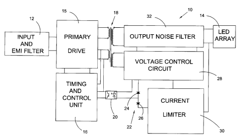
6 [0017] Referring now to the figures, Figure 1 shows a simplified schematic
of an LED
7 driver according to the current invention. LED driver 10 includes input 12
and output 14 on
8 opposite sides of the circuit. The input could be arranged to receive
alternating or direct current.
9 The input may also include an electromagnetic interference (EMI) filter for
reducing any
disturbance caused any electromagnetic or radio frequency interference.
11 [0018] Primary drive 15 is connected to the input 12 and controlled by
timing and control
12 unit 16. The timing and control unit uses, for example, pulse width
modulation (PWM) to control
13 the output of primary drive 15 to transformer 18. The timing and control
unit is also arranged to
14 receive signals via optocoupler 20. Optocouplers are also known as opto-
isolators,
photocouplers, or optical isolators, and their general use is known in the art
for transmitting
16 electrical signals in the form of light between two otherwise electrically
isolated circuits. Thus,
17 the input, primary drive, and timing and control unit are isolated from the
output side of driver 10
18 via transformer 18 and optocoupler 20. The optocoupler is also connected on
the output side of
19 driver 10 to junction 22, which includes diode 24 and diode 26. Diode 24 is
included to close
voltage control loop or circuit 28, while diode 26 is included to close
current limiting loop 30.
21 Voltage control loop 28 and current limiting loop 30 may simply be referred
to as the voltage loop
22 and current loop, respectively. Output noise filter 32 is included,
including, for example, a
23 plurality of e-caps, as described in more detail below to filter ripple
current noise and the like
24 from the system.
[0019] Generally, voltage control loop 28 is included to monitor the feedback
voltage
26 from LED array 14 in case the feedback voltage rises over a predetermined
maximum. If the
27 feedback voltage from the LEDs increases over a predetermined maximum, the
voltage control
28 loop will communicate this unbalancing to current limiting loop 30. Current
limiting loop 30
29 regulates the output current to the LED array. As described above, it is
important for the current
running through to the LEDs to remain constant because the current determines
the brightness
31 of the LEDs. The current limiting loop may, for example, regulate the
current by comparing a
32 measured voltage with a reference voltage, taking into account the feedback
voltage monitored
22052793.2 5
CA 02721768 2010-11-17
Agent Ref.: 77136/00002
1 by, the voltage loop, and altering the output voltage to LED array 14 so
that the measured
2 voltage remains within a certain predetermined acceptable range of the
reference voltage. In
3 this way, constant output current can be maintained through the LED array.
4 [0020] Voltage control loop is also included in the event that one or more
LEDs in LED
array 14 shorts or burns out. The reference voltage is determined based on a
full array of
6 functioning LEDs. If one LED burns out, then there will be no voltage drop
over that LED, and
7 the measured output voltage will be unnecessarily high. If the output
voltage to the remaining
8 LEDs becomes unnecessarily high, the likely result is that the remaining
LEDs suffer premature
9 burn out. Since prior art systems are only concerned with maintaining a
constant output current,
these prior art drivers would continue maintaining the constant predetermined
current based on
11 the same reference voltage, regardless of the number of LEDs that have
burned or shorted out.
12 Based on the determination of unnecessarily high voltage by voltage loop
28, optocoupler 20 will
13 send a corresponding signal to timing circuit 16. The signal from
optocoupler 20 will cause the
14 timing circuit to, for example, lower the operating frequency of the
circuit, which will drop the
input voltage received by input 12.
16 [0021] As one example, if several LEDs in an array, such as array 14, are
to burn out,
17 the power required by the system may drop from 36W to 30W. The signal from
the optocoupler
18 will instruct timing circuit 16 that this drop from 36W to 30W is
necessary, and the input voltage
19 will drop accordingly due to a change in the operating frequency set by the
timing unit. Since the
input voltage is dropped, the total power consumed by the system is kept to a
minimum, thereby
21 maintaining a potentially longer lifespan for the remaining LEDs and other
driver components.
22 [0022] Accordingly, if the voltage to the LEDs raises higher than the
required set output
23 voltage, for example by a diode failing in an open mode of operation,
circuit 10 will automatically
24 self adjust both the current and voltage to the LED array in order to
maintain maximum allowable
values for the voltage and current. Additionally, if an LED is shorted in a
closed mode of
26 operation, the current to the LEDs will become unnecessarily high, and the
circuit will also self
27 adjust the current to the LEDs. It should thus be appreciated that driver
10 offers two levels of
28 protection to the LEDs by utilizing a dual closed loop design that
simultaneously monitors both
29 the current and the voltage sent to the LEDs and by permitting
communication between the
loops such that the current loop can take into account the voltages monitored
by the voltage
31 loop. Heretofore, only one parameter, the voltage or the current, but not
both, could be
32 monitored and controlled at a time.
22052793.2 6
CA 02721768 2010-11-17
Agent Ref.: 77136/00002
1 [0023] Further advantages can be appreciated in view of the more detailed
embodiment
2 of driver 10 shown in Figure 2. In this embodiment, the basic components
shown in Figure 1 are
3 included, such as input 12, output 14, primary driver 15, timing unit 16,
transformer 18,
4 optocoupler 20, junction 22 including diodes 24 and 26, voltage loop 28, and
current loop 30.
Various other components, such as resistors, capacitors, integrated circuits,
inductors, etc. are
6 shown in Figure 2. These additional components are shown both with standard
symbols and
7 labeled with an alphanumeric identifiers. For example, capacitors are
indicated by the
8 commonly known symbol '11' and are labeled C1, C2, C3, etc. In view of these
symbols and
9 identifiers, a discussion of each individual component is not necessary, as
one of ordinary skill in
the art can appreciate the general purpose of each of those components not
otherwise
11 specifically discussed herein. It should be appreciated with respect to
Figure 2 that any four way
12 intersection of wires (that is, resembling a '+') indicates a crossing of
the wires, not a node,
13 except where indicated by a bold dot (that is, resembling a '='), which dot
does indicate a node.
14 Like the dot, any three-way intersection (that is, resembling a 'T')
indicates a connection or node
between the wires.
16 [0024] In the embodiment of Figure 2, input 12 receives a voltage input
from an AC
17 source. Output array 14 is comprised of LEDs 34, which are arranged in
banks, columns, or
18 rows. One such bank is shown in Figure 2, including ten LEDs 34 connected
in series. It should
19 be appreciated that any number of LEDs could be included in each bank, and
any number of
banks could be included connected in parallel in array 14, but that array 14
should include at
21 least one LED. The AC voltage input is transferred to primary drive 15,
such as via a bridge
22 rectifier (e.g., bridge rectifier BR1, which may have part number KBP21OG
or any other suitable
23 component), which is further transferred via transformer 18 to the output,
thereby isolating the
24 input from the output. Timing circuit 16 operates, for example, by pulse
width modulation
(PWM), and may include a transition mode PFC controller 38 (also generally
labeled U1, which
26 may have part number L6562) and power MOSFET 40 (also generally labeled Q1,
which may
27 have part number 7N80) in order to control an operating frequency of the
circuit. It has been
28 found that selecting components with low switching noise, such as by those
part numbers
29 indicated, increases desired performance. It should of course be
appreciated that other
components could be used as necessary for individual applications and that the
schematic of
31 Figure 2 is provided as one example only.
32 [0025] Timing unit 16 is in communication with voltage circuit 28 via
optocoupler 20,
33 such that the optocoupler can send signals to the timing unit when the
voltage loop detects
22052793.2 7
CA 02721768 2010-11-17
Agent Ref.: 77136/00002
1 improperly high feedback voltages, as described above. Diodes 24 and 26
(also generally
2 labeled D8 and D9, respectively, which both may have part number LL4148) are
included at
3 junction 22 to close the voltage loop and current loop, respectively.
However, as described
4 above, the voltage loop and current loop are kept in communication such that
the current loop
can take into account the feedback voltage levels that are monitored by the
voltage loop in order
6 to more effectively regulate the output current. For example, current loop
30 includes a dual
7 operational amplifier, which may be included in voltage reference monolithic
integrated circuit 36
8 (also generally labeled U3, which may have part number TSM103W). Integrated
circuit 36
9 regulates the current by comparing a measured voltage with a reference
voltage, and altering
the output voltage to LED array 14 such that the measured voltage remains
within a certain
11 predetermined acceptable range of the reference voltage in order to
maintain a constant output
12 current through the LED array. Since a constant current is required to
maintain proper
13 functioning of typical LEDs, integrated circuit 36 will likely be
constantly making adjustments to
14 the output voltage to maintain a constant current through the LEDs during
operation of driver 10.
[0026] In addition to self-regulating the output voltage and current to the
LEDs, circuit 10
16 is designed to also enable longer life of the e-caps, specifically, the
output filtering capacitors in
17 noise filter 32 (see, for example, the capacitors labeled C14 and C24).
Noise is created by the
18 components of circuit 10, such as timing circuit 16 and integrated circuit
36, as these
19 components switch on and off. For this reason, parts should be selected
which have low noise
characteristics, such as those part numbers identified above, but it should be
understood that
21 other parts could be substituted for these specific part models, especially
other models which
22 result in low ripple current noise. Particularly during startup, there is
an in rush or spike of high
23 frequency current to the LEDs, which should be filtered for better
performance. The filtering
24 capacitors are included for this purpose, but it is still important to keep
the ripple current through
the capacitors to a minimum to ensure a longer life.
26 [0027] Furthermore, LC loop 42 may be included having an inductor (for
example, the
27 inductor labeled L1) and a capacitor (for example, the capacitor labeled
C15) to provide
28 enhanced filtering of noise before the current is output to the LEDs. In
addition, buffering unit 46
29 may be provided between opposite sides of transformer 18, such as by use of
capacitor (for
example, the capacitor generally labeled C20). Buffering unit 46 is provided
in conjunction with
31 RC loop 44, which includes a resistor (for example, the resistor generally
labeled R26) and a
32 capacitor (for example, the capacitor generally labeled C13) applied across
a pair of diodes (for
33 example, the diodes generally labeled D5). A large capacitance is desired
for buffering unit 46,
22052793.2 8
CA 02721768 2010-11-17
Agent Ref.: 77136/00002
1 however, large capacitances significantly slow down the speed of the
circuit. Advantageously,
2 including RC loop 44 enables a much smaller capacitance to be used for
buffering unit 46, so
3 that spikes and noise will be filtered primarily through the RC loop,
thereby preventing overly
4 reducing the speed of the circuit.
[0028] It should again be appreciated that the above specific embodiment
should not be
6 considered to limit the scope of the current invention, but instead only to
exemplify one particular
7 embodiment of a circuit for a power supply which can be used to drive an
array of LEDs. The
8 power supply disclosed in Figure 2 is intended to be variable between 5W and
140W, as needed
9 to power arrays of LEDs of different sizes and configurations. The shown
circuit may have an
operating frequency of 120 Hz, a power factor of about 95.95, and regulate an
output voltage to
11 the LEDs to .7V peak to peak. Drivers according to the current invention
and as exemplified in
12 Figure 2 are capable of maintaining a lifespan of at least approximately
75,000 hours (before
13 failure or unacceptable brightness degradation) at 80 C due to the unique
selection and
14 arrangement of parts to reduce noise to the e-caps, and self-regulation of
both the output and
voltage and current, versus prior art power supplies which are only rated for
only about 40,000
16 hours at this temperature. One of ordinary skill in the art will readily
appreciate that there are
17 numerous ways to arrange components in an electronic circuit, and that the
benefits of a dual
18 closed loop voltage and current regulating arrangement and low noise
maintenance techniques
19 could be utilized by any number of circuit designs. As such, more or less
resistors, capacitors,
diodes, and other components, or the same number of these components having
different
21 values, could be included, as desired, for each individual application of
the current invention
22 principles.
23 [0029] Thus, it is seen that the objects of the present invention are
efficiently obtained,
24 although modifications and changes to the invention should be readily
apparent to those having
ordinary skill in the art, which modifications are intended to be within the
spirit and scope of the
26 invention as claimed. It also is understood that the foregoing description
is illustrative of the
27 present invention and should not be considered as limiting. Therefore,
other embodiments of
28 the present invention are possible without departing from the spirit and
scope of the present
29 invention.
22052793.2 9