Note: Descriptions are shown in the official language in which they were submitted.
CA 02722436 2015-12-11
TITLE: SINGLE SWITCH HIGH EFFICIENCY POWER SUPPLY
PRIORITY CLAIM
[0001] This application claims the benefit of previously filed U.S.
Provisional Patent
Application entitled "Single Switch Unregulated Inductorless High Voltage High
Efficiency Power Supply," assigned USSN 61/057,589, filed May 30, 2008 and
U.S.
Utility Patent Application entitled "Single Switch High Efficiency Power
Supply,"
assigned USSN 12/472,774 filed May 27, 2009.
FIELD OF THE INVENTION
[0002] The present subject matter relates to power supplies. More
particularly, the
present subject matter relates to a series charge, parallel discharge
capacitor power
supply requiring only a single switch and no inductor in order to shift from
charge
mode to discharge mode.
BACKGROUND OF THE INVENTION
[0003] Power supplies constructed using the known concept of serially
charging a
series of capacitors and discharging the series in parallel are known in the
art. Such
configurations may be used, for example, with variations in excitation, for a
variety of
configurations. In one example, U.S. Patent No. 5,446,644 (Zhou) discloses a
direct
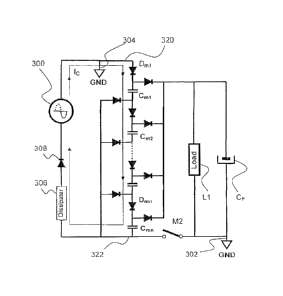
current (DC) voltage divider configuration employing a diode and capacitor
configuration very similar to that illustrated herein in Figures 1 and 2. In
such '644
Patent configuration, a DC supply is applied as the input to a diode and
capacitor
series circuit by way of a first switch. A second switch is configured to
couple a
number of diodes to the series connected capacitors to provide a parallel
discharge
path. Generally, such arrangement operates as a voltage divider in order to
convert a
relatively higher DC voltage to a relatively lower DC voltage. With an input
DC
voltage to such circuit, Zhou operates the switches alternately at
1
CA 02722436 2010-10-22
WO 2009/155018 PCT/US2009/045380
a frequency chosen to produce a desired output voltage level. Such form of
operation results in a somewhat selectively variable output voltage but at the
cost
of complex variable frequency alternating operation of such two switches.
[0004] In a somewhat similar arrangement, Cubbison, Jr. (U.S. Patent No.
4,649,468) discloses a voltage divider circuit employing a series
charge/parallel
discharge diode/capacitor circuit where the diodes provide the switching
without
additional switches. The circuit in such Cubbison, Jr. arrangement, however,
provides sub-divided capacitors, with varying numbers of capacitors used
directly
connected in series to provide desired low voltage outputs.
[0005] An "Analog Devices" article illustrates the use of a capacitor
divider
power supply in an electric meter. See, Analog Devices Application Note AN-
687,
"A Low Cost Tamper-Resistant Energy Meter Based on the ADE7761 with Missing
Neutral Function" by English and Moulin, 2004, including material starting on
page
7 of such publication under the title "Power Supply Design." A Linear
Technology
Magazine article illustrates a switch capacitor voltage regulator that is
configured
to provide current gain. See, Design Ideas, "Switched Capacitor Voltage
Regulator Provides Current Gain" Linear Technology Magazine, February 1999.
[0006] Despite some benefits offered by such configurations and others,
it
would, nevertheless, be beneficial to provide a simplified series-parallel
capacitor-
diode voltage dividing circuit that was able to produce a regulated low DC
voltage
based on a higher level alternating current (AC) input source.
[0007] While various implementations of series-parallel capacitor-diode
voltage
dividing circuits have been developed, and while various combinations of AC to
DC
and DC to DC voltage divider circuits have been developed, no design has
emerged that generally encompasses all of the desired characteristics as
hereafter
presented in accordance with the subject technology.
SUMMARY OF THE INVENTION
[0008] In view of the recognized features encountered in the prior art and
addressed by the present subject matter, an improved single switch series-
parallel
capacitor-diode voltage dividing circuit has been provided.
2
CA 02722436 2016-11-03
10009] In an exemplary configuration, a voltage divider for converting
high voltage
alternating current (AC) into a relatively lower direct current (DC) regulated
supply is
provided. The voltage dividing power supply includes a plurality of capacitors
connected in series with a plurality of diodes for charging the capacitors,
and a
second plurality of diodes coupled to each of the series connected capacitors
and to a
single switch for discharging the capacitors.
[0010] In one of their simpler forms, capacitive voltage dividers having
input and
output portions where the input portion is configured for unidirectional
transmission of
current from an input source to the capacitive divider and the input and
output
portions of the divider are configured to operate alternately.
[0011] One present exemplary embodiment relates to a power supply for
reducing
a relatively high level alternating current (AC) from an AC input source to a
relatively
lower level direct current (DC), comprising a voltage divider and a means for
controlling operation of a single switching element. Preferably, such
exemplary
voltage divider may be configured as a series of capacitors and diodes, the
voltage
divider including a single switching element and no inductor to shift from a
charge
mode for series charging the capacitors to discharge mode for parallel
discharging the
capacitors, wherein the voltage divider includes a plurality of capacitors
connected in
series with a first plurality of diodes for charging the capacitors, and a
second plurality
of diodes coupled to each of the series connected capacitors and to the single
switching element for discharging the capacitors, with such voltage divider
having
respective input and output portions, the input portion connected to the AC
input
source for unidirectional transmission of current from the AC input source to
the
capacitive divider, and with the input and output portions of the divider
configured to
operate alternately, wherein the series capacitors and the first plurality of
diodes
comprise an alternating series string of capacitors and diodes beginning with
a diode
and ending with a capacitor; a first ground reference connection connected to
the
beginning of the alternating series string, and a second ground reference
connected
to the end of the alternating series by the single switch element during a
discharge
mode of the power supply; and such means for controlling the single switching
element is provided to charge the capacitor series during the negative half
cycle of the
3
CA 02722436 2016-11-03
AC input source when the single switching element is open and to discharge the
capacitors during the positive half cycle thereof when the single switching
element is
closed, thereby producing a relatively low DC voltage based on the relatively
higher
level AC input source.
[0012] In various forms of the foregoing exemplary embodiment, such voltage
divider may include a plurality of capacitors connected in series with a first
plurality of
diodes for charging the capacitors, and a second plurality of diodes coupled
to each of
the series connected capacitors and to a single switch element for discharging
the
capacitors, with such voltage divider configured for having respective input
and output
portions, with such input portion configured for unidirectional transmission
of current
from the input source to the capacitive divider, and with the input and output
portions
of the divider configured to operate alternately. Still, in further
variations, such series
3a
CA 02722436 2015-12-11
capacitors and such first plurality of diodes may comprise an alternating
series string
beginning with a diode and ending with a capacitor; and such power supply may
further include a first ground reference connection connected to the beginning
of such
alternating series string, and a second ground reference connected to the end
of such
alternating series by such single switch element during a discharge mode of
such
power supply.
10013] In some embodiments of the foregoing, such power supply may
further
include a load associated with discharge of such voltage divider, and a filter
capacitor
in parallel with such load, to provide ripple filtering and to assist in
voltage regulation
of the low voltage DC produced by discharge of such voltage divider.
[0014] Still further, such an exemplary present power supply may
optionally
include circuitry for automatically switching such voltage divider between
charge and
discharge cycles thereof; and wherein such circuitry may include a voltage
comparator and a reference, for comparing the voltage output of such power
supply
with such reference.
[0015] Such present exemplary power supply embodiments in some
variations
thereof may further include a series diode and a dissipater element in series
with the
AC input source and such alternating series string. Still further, in some
embodiments, the AC input source corresponds to about a 400 VAC input voltage,
and the voltage output of such power supply is about 5 VDC.
[0016] Another present exemplary embodiment may relate to a power supply
for
reducing a relatively high level alternating current (AC) from an AC input
source of up
to about 500 VAC to a relatively lower level direct current (DC) of less than
about 10
VDC, comprising a voltage divider including a plurality of capacitors
connected in
series with a first plurality of diodes for charging the capacitors from the
AC input
source with unidirectional transmission of current from the AC input source to
the
voltage divider, with such series capacitors and such first plurality of
diodes
comprising an alternating series string of capacitors and diodes beginning
with a
diode and ending with a capacitor, and such voltage divider including a second
plurality of diodes coupled to each of the series connected capacitors and to
a single
switch element for alternately discharging the capacitors into an associated
output
4
CA 02722436 2016-11-03
load; a first ground reference connection connected to the beginning of such
alternating series string; a second ground reference connected to the end of
such
alternating series by such single switch element during a discharge mode of
such
power supply; and circuitry for automatically switching such single switching
element,
wherein when the single switching element is open, the plurality of capacitors
charge
during the negative half cycle of the AC input source and when the single
switching
element is closed, the plurality of capacitors discharge during the positive
half cycle
thereof, thereby producing a relatively low DC voltage based on the relatively
higher
level AC input source.
[0017] Some variations of the foregoing may further include a series diode
and a
dissipater element in series with the AC input source and such alternating
series
string. Still further, others may include a filter capacitor in parallel with
the output
load, to provide ripple filtering and to assist in voltage regulation of the
low voltage DC
produced by discharge of such voltage divider; and wherein the AC input source
corresponds to about a 400 VAC input voltage, and the voltage output of such
power
supply is about 5 VDC. Other present exemplary variations may include such
exemplary circuitry including a voltage comparator and a reference, for
comparing the
voltage output of such power supply with such reference.
[0018] It should be also understood and appreciated that the present
subject
matter equally relates to corresponding methodologies and related apparatuses.
[0019] One present exemplary method encompasses power supply methodology
for reducing a relatively high level alternating current (AC) from an AC input
source to
a relatively lower level direct current (DC), comprising providing a voltage
divider
configured as a series of capacitors and diodes arranged for series charging
of the
capacitors and parallel discharge thereof by way of a single switching element
and no
inductor in order to shift from charge mode to discharge mode, wherein
providing
such voltage divider includes providing a plurality of capacitors connected in
series
with a first plurality of diodes for charging the capacitors as an alternating
series string
of capacitors and diodes, and a second plurality of diodes coupled to each of
the
series connected capacitors and to a single switch element for discharging the
capacitors, with such voltage divider configured for having respective input
and output
5
CA 02722436 2016-11-03
portions, with such input portion configured for unidirectional transmission
of current
from the input source to the capacitive divider, and with the input and output
portions
of the divider configured to operate alternately, and wherein the series
capacitors and
first plurality of diodes comprise an alternating series string of capacitors
and diodes
beginning with a diode and ending with a capacitor; providing a first ground
reference
connection connected to the beginning of the alternating series of first
plurality of
diodes and series capacitors; providing a second ground reference connected to
the
end of such alternating series by such single switch element during a
discharge mode
of such power supply; and providing a series diode and a dissipater element in
series
with an AC input source and the alternating series string; and controlling
operation of
the single switching element, wherein when the single switching element is
open, the
capacitor series charges during the negative half cycle of the AC input source
and
when the single switching element is closed, the capacitors discharge during
the
positive half cycle thereof, thereby producing a relatively low DC voltage
based on the
relatively higher level AC input source.
100201 In present variations of such present methodology, providing such
voltage
divider may include providing a plurality of capacitors connected in series
with a first
plurality of diodes for charging the capacitors, and a second plurality of
diodes
coupled to each of the series connected capacitors and to a single switch
element for
discharging the capacitors, with such voltage divider configured for having
respective
input and output portions, with such input portion configured for
unidirectional
transmission of current from the input source to the capacitive divider, and
with the
input and output portions of the divider configured to operate alternately.
5a
CA 02722436 2010-10-22
WO 2009/155018 PCT/US2009/045380
[0021] In other present variations such power supply methodology may
include
the series capacitors and first plurality of diodes comprising an alternating
series
string beginning with a diode and ending with a capacitor; and such power
supply
methodology further including providing a first ground reference connection
connected to the beginning of the alternating series of first plurality of
diodes and
series capacitors; providing a second ground reference connected to the end of
such alternating series by such single switch element during a discharge mode
of
such power supply; and providing a series diode and a dissipater element in
series
with an AC input source and the first plurality of diodes/series capacitor
charging
string.
[0022] In exemplary variations of the present power supply methodology,
charging of the plurality of capacitors may be achieved during the negative
half
cycle of the AC input source by coupling an upper end of the first plurality
of diodes
to a ground potential and by forcing such ground potential to be relatively
positive
with respect to a lower end of the first plurality of diodes/capacitor string
as the
output of the AC input source goes through its negative half cycle;
discharging of
the plurality of capacitors may be achieved during the positive half cycle of
the AC
input source by closing the single switching element so as to discharge the
plurality of capacitors through the second plurality of diodes, into a load
associated
therewith; and such power supply methodology may further include providing a
filter capacitor in parallel with such load, to provide ripple filtering and
to assist in
voltage regulation of the low voltage DC produced by discharge of the
capacitive
voltage divider.
[0023] Other present exemplary variations of the subject power supply
methodology may further include providing circuitry for automatically
switching the
capacitive voltage divider between charge and discharge cycles thereof. In
certain
instance, such exemplary circuitry may include a voltage comparator comparing
the voltage output of such power supply with a reference; and such power
supply
methodology may further include using an optical isolation device, and peak
tracking of the voltage output, to provide relatively high efficiency
switching
operations. In other present variations, the AC input source may correspond to
about a 400 VAC input voltage, and the voltage output of such power supply may
be about 5 VDC.
6
CA 02722436 2010-10-22
WO 2009/155018 PCT/US2009/045380
[0024] Additional objects and advantages of the present subject matter
are set
forth in, or will be apparent to, those of ordinary skill in the art from the
detailed
description herein. Also, it should be further appreciated that modifications
and
variations to the specifically illustrated, referred and discussed features,
elements,
and steps hereof may be practiced in various embodiments and uses of the
present subject matter without departing from the spirit and scope of the
subject
matter. Variations may include, but are not limited to, substitution of
equivalent
means, features, or steps for those illustrated, referenced, or discussed, and
the
functional, operational, or positional reversal of various parts, features,
steps, or
the like.
[0025] Still further, it is to be understood that different embodiments,
as well as
different presently preferred embodiments, of the present subject matter may
include various combinations or configurations of presently disclosed
features,
steps, or elements, or their equivalents (including combinations of features,
parts,
or steps or configurations thereof not expressly shown in the figures or
stated in
the detailed description of such figures). Additional embodiments of the
present
subject matter, not necessarily expressed in the summarized section, may
include
and incorporate various combinations of aspects of features, components, or
steps
referenced in the summarized objects above, and/or other features, components,
or steps as otherwise discussed in this application. Those of ordinary skill
in the
art will better appreciate the features and aspects of such embodiments, and
others, upon review of the remainder of the specification.
BRIEF DESCRIPTION OF THE DRAWINGS
[0026] A full and enabling disclosure of the present subject matter,
including the
best mode thereof, directed to one of ordinary skill in the art, is set forth
in the
specification, which makes reference to the appended figures, in which:
[0027] Figure 1 illustrates a known series-charge, parallel-discharge
capacitive
voltage divider specifically illustrating the charging portion of a charge-
discharge
cycle;
[0028] Figure 2 illustrates the same circuit illustrated in Figure 1 but
specifically
illustrating the discharge portion of a charge-discharge cycle;
7
CA 02722436 2010-10-22
WO 2009/155018 PCT/US2009/045380
[0029] Figure 3 illustrates an exemplary voltage divider embodiment in
accordance with the present technology, and specifically illustrating the
charge
portion of the present charge-discharge cycle subject matter;
[0030] Figure 4 illustrates the exemplary voltage divider embodiment in
accordance with the present technology as illustrated in present Figure 3, but
specifically illustrating the discharge portion of the present charge-
discharge cycle
subject matter;
[0031] Figure 5 illustrates an alternative voltage divider embodiment in
accordance with the present technology, and including circuitry for
automatically
switching between the charge and discharge portions of the present cycle
subject
matter; and
[0032] Figure 6 graphically illustrates a present example of charge
build up
across a load and parallel filter capacitor from a high voltage input to the
voltage
divider in accordance with the present technology.
[0033] Repeat use of reference characters throughout the present
specification
and appended drawings is intended to represent same or analogous features,
elements, or steps of the present subject matter.
DETAILED DESCRIPTION OF THE PREFERRED EMBODIMENTS
[0034] As referenced in the Summary of the Invention section, the
present
subject matter is particularly concerned with an improved single switch series-
parallel capacitor-diode voltage dividing circuit.
[0035] Selected combinations of aspects of the disclosed technology
correspond to a plurality of different embodiments of the present subject
matter. It
should be noted that each of the exemplary embodiments presented and
discussed herein should not insinuate limitations of the present subject
matter.
Features or steps illustrated or described as part of one embodiment may be
used
in combination with aspects of another embodiment to yield yet further
embodiments. Additionally, certain features may be interchanged with similar
devices or features not expressly mentioned which perform the same or similar
function.
8
CA 02722436 2010-10-22
WO 2009/155018
PCT/US2009/045380
[0036] Referring now to the drawings, and with initial reference to
Figures 1 and
2, there is illustrated the operation of a generally known capacitive divider
circuitry.
As illustrated in Figures 1 and 2, a capacitive voltage divider having a
plurality of
series coupled capacitors C1, C2, ... Cn coupled alternately in series with a
plurality
of diodes Dci, Dc2 Dcn has been
provided. An input source G is provided to
supply charging current lc to the series coupled capacitors C1, C2, ... Cn by
way of
a first switch K1 and the plurality of diodes DC1, DC2 Dc.
[0037] It will be appreciated that during a capacitor charging period,
first switch
K1 is closed while a second switch K2, coupled to a load, is opened. It should
be
further appreciated that the charging circuit is functional regardless of
whether
source G corresponds to either an AC or DC supply; however, if source G is
provided as an AC supply, charging and operation of first switch K1 must be
coordinated with the positive half cycle of the AC source while discharging of
the
capacitors and operation of second switch K2 must be coordinated with the
negative half cycle of the AC source.
[0038] With reference to Figure 2, it will be noted that second switch
K2 is
coupled to the load and to a second plurality of diodes DDi, DD2,
DDn such that,
upon closure of switch K2, and concurrent opening of switch K1, charge stored
in
series coupled capacitors C1, C2, ... Cn during the charging portion of the
cycle
store is discharged by way of the second plurality of diodes DDi, DD2, Dlin
to
provide a plurality of current flows IDi, ID2 IDn through the load, thereby
effectively providing discharge of all of the capacitors in parallel through
the load.
[0039] Reference will now be made in detail to the presently preferred
embodiments of the subject series-parallel capacitor-diode voltage dividing
circuit.
Initially with reference to Figures 3 and 4, there are illustrated and
represented a
capacitive voltage divider and its operation in accordance with present
technology.
A comparison of Figures 3 and 4 with Figures 1 and 2 reflects that there are a
number of differences among the illustrations. In a first instance, while both
of the
series capacitor and diode strings begin with a diode, the diode/capacitor
string in
accordance with the present subject matter ends with a capacitor as compared
to
the known configuration ending with a diode. In a second instance, the subject
matter of the present technology provides a pair of ground reference
connections
302, 304 whose functions will be described further hereinbelow. Thirdly, the
9
CA 02722436 2010-10-22
WO 2009/155018
PCT/US2009/045380
configuration of the present technology provides a series diode 308 and
dissipater
element 306 in series with AC input source 300 and the charging portion of the
diode/capacitor string corresponding to a first plurality of diodes Dmi
Dmn and a
plurality of intervening capacitors Cmi
Cmn. As a result of the foregoing, and as
a further difference, the capacitive voltage divider of the present technology
is
configured to provide its functionality based on the operation of a single
switch M2
instead of the pair of switches K1, K2 previously required.
[0040] Operational aspects of a voltage dividing circuit constructed in
accordance with the present technology are described with further reference to
Figure 3. As previously noted, the voltage divider of the present technology
provides an AC input source 300 coupled to the capacitor/diode charging string
corresponding to diodes Dmi ... D. and capacitors Cmi
Cmn by way of a diode
308 and dissipater element 306, without requiring or making use of any switch
equivalent to switch K1 of the previously know configuration of Figures 1 and
2.
[0041] In the case
of the present technology, charging of capacitors Cmi Cmn
is achieved during the negative half cycle of the AC. This is accomplished by
coupling the upper end 320 of the diode/capacitor string to ground potential
304
and by forcing that ground potential to be relatively positive with respect to
the
lower end 322 of the diode/capacitor string as the output of AC source 300
goes
through its negative half cycle.
[0042]
With the upper end 320 of the diode/capacitor string more positive than
the lower end 322 thereof, charging current flow lc passes through the
diode/capacitor string to charge the series coupled capacitors in a current
flow
fashion generally similar to that of the known configurations yet entirely
without the
use of a switching element such as switch K1 as previously employed. When the
output of AC source 300 goes through its positive half cycle, switch M2 is
closed
and then charged capacitors are discharged in parallel by way of diodes Dn1
Dnn
and Dp1 Dpn forming discharge currents 1111,102,
IDn through load Ll . In one
exemplary embodiment of the present technology, a filter capacitor CF may be
provided in parallel with load L1 to provide ripple filtering and to assist in
voltage
regulation of the low voltage DC produced by operation of the capacitive
voltage
divider in accordance with present technology.
CA 02722436 2010-10-22
WO 2009/155018 PCT/US2009/045380
[0043] With reference now to Figure 5, there is illustrated a capacitive
voltage
divider in accordance with a further exemplary embodiment of the present
subject
matter, and including circuitry for automatically switching between the charge
and
discharge portions of the cycle. As illustrated in Figure 5, an exemplary
voltage
comparator 510 monitors the output voltage at line 512 (representing the
voltage
across the load) and compares such output voltage to a reference REF. As the
output voltage at line 512 reaches a maximum voltage, exemplary switch M2 is
opened under the control of an output 514 from voltage comparator 510.
[0044] Those of ordinary skill in the art will appreciate that switch M2
may
correspond to a solid state switching device or may comprise more complex
switching circuit, while voltage comparator 510 and reference source REF may
also correspond to more complex configurations. For example, switch circuitry
corresponding to illustrated switch M2 may include such as optical isolation
devices, while voltage comparator 510 and reference source REF may provide for
peak tracking of output voltage from monitored line 512 to provide higher
efficiency
for the switching operation illustrated as and/or represented by
diagrammatical
switch M2.
[0045] With reference now to Figure 6, there are graphically illustrated
voltage
waveforms illustrating the operation of an exemplary voltage divider in
accordance
with the present technology. As may be seen from such graph, input voltage 610
may correspond, for example, to a high voltage AC from one phase of a multi-
phase source. In an exemplary configuration, input voltage 610 may correspond
to
a 400 VAC input voltage that is to be reduced to, for example, approximately 5
VDC for operation, for example, of a load device or circuit.
[0046] Output voltage 620 of Figure 6 is graphically illustrated as a
filtered DC
voltage as produced from an exemplary voltage divider in accordance with
present
technology. Those of ordinary skill in the art will appreciate that while the
two
traces illustrated share the same time frame, the magnitude of the traces are
illustrative only and are not illustrated to the same scale. As noted
previously,
trace 610 representing the input voltage is representative of, for example, a
400
VAC input while trace 620 representing the output of the subject voltage
divider
may correspond to about 5 VDC. It should be further appreciated that alternate
11
CA 02722436 2010-10-22
WO 2009/155018 PCT/US2009/045380
input and output voltage levels are possible within the spirit and scope of
the
present technology.
[0047] While the present subject matter has been described in detail
with
respect to specific embodiments thereof, it will be appreciated that those
skilled in
the art, upon attaining an understanding of the foregoing, may readily produce
alterations to, variations of, and equivalents to such embodiments.
Accordingly,
the scope of the present disclosure is by way of example rather than by way of
limitation, and the subject disclosure does not preclude inclusion of such
modifications, variations and/or additions to the present subject matter as
would be
readily apparent to one of ordinary skill in the art.
12