Note: Descriptions are shown in the official language in which they were submitted.
CA 02722451 2010-10-22
WO 2009/132358 PCT/US2009/041851
PHASED-ARRAY ANTENNA PANEL
FOR A SUPER ECONOMICAL BROADCAST SYSTEM
CROSS-REFERENCE TO RELATED APPLICATIONS
[0001] This application claims priority to U.S. Provisional Patent Application
Serial
No. 61/047,772 (entitled "Phased-Array Antenna Panel For a Super Economical
Broadcast
System," filed on April 25, 2008), the contents of which is incorporated
herein by reference
in its entirety.
FIELD OF THE INVENTION
[0002] The present invention relates, generally, to cellular communication
systems.
More particularly, the present invention relates to a phased-array antenna
panel.
BACKGROUND OF THE INVENTION
[0003] Cellular radiotelephone system base transceiver stations (BTSs), at
least for
some United States (U.S.) and European Union (EU) applications, may be
constrained to a
maximum allowable effective isotropically radiated power (EIRP) of 1640 watts.
EIRP, as a
measure of system performance, is a function at least of transmitter power and
antenna gain.
As a consequence of restrictions on cellular BTS EIRP, U.S., EU, and other
cellular system
designers employ large numbers of BTSs in order to provide adequate quality of
service to
their customers. Further limitations on cells include the number of customers
to be served
within a cell, which can make cell size a function of population density.
[0004] One known antenna installation has an antenna gain of 17.5 dBi, a
feeder line
loss of 3 dB (1.25" line, 200 ft mast) and a BTS noise factor of 3.5 dB, such
that the Ga -
NFsys = 17.5 - 3.5 - 3.0 = 11 dBi (in uplink). Downlink transmitter power is
typically 50 W.
With feeder lines, duplex filter and jumper cables totaling -3.5 dB, the Pa
input power to
antenna is typically 16 W, such that the EIRP is 16 W + 17.5 dB = 1,000 W.
[0005] In many implementations, each BTS is disposed near the center of a
cell,
variously referred to in the art by terms such as macrocell, in view of the
use of still smaller
-1-
CA 02722451 2010-10-22
WO 2009/132358 PCT/US2009/041851
cells (microcells, nanocells, picocells, etc.) for specialized purposes such
as in-building or in-
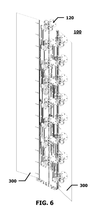
aircraft services. Typical cells, such as those for city population density,
have radii of less
than 3 miles (5 kilometers). In addition to EIRP constraints, BTS antenna
tower height is
typically governed by various local or regional zoning restrictions.
Consequently, cellular
communication providers in many parts of the world implement very similar
systems.
[0006] Restrictions on cellular BTS EIRP and antenna tower height vary within
each
countries. Not only is the global demand for mobile cellular communications
growing at a
fast pace, but there are literally billions of people, in technologically-
developing countries
such as India, China, etc., that currently do not have access to cellular
services despite their
willingness and ability to pay for good and inexpensive service. In some
countries,
government subsidies are currently facilitating buildout, but minimization of
the cost and
time for such subsidized buildout is nonetheless desirable. In these
situations, the problem
that has yet to be solved by conventional cellular network operators is how to
decrease
capital costs associated with cellular infrastructure deployment, while at the
same time
lowering operational expenses, particularly for regions with low income levels
and/or low
population densities. An innovative solution which significantly reduces the
number of
conventional BTS site-equivalents, while reducing operating expenses, is
needed.
SUMMARY OF THE INVENTION
[0007] Embodiments of the present invention provide a phased-array antenna
panel
for a super economical broadcast system.
[0008] In one embodiment, a phased-array antenna panel system includes an
antenna
panel support member, a first pair of striplines and a second pair of
striplines. The antenna
panel support member includes a front reflector surface to support first and
second columns
of constantly-spaced, crossed-dipole radiators, a first pair of signal ground
cavities disposed
beneath the first column of crossed-dipole radiators, a second pair of signal
ground cavities
disposed beneath the second column of crossed-dipole radiators, and a rear
surface including
first and second pairs of signal distribution cable connectors. The first pair
of striplines are
respectively disposed within the first pair of signal ground cavities and are
coupled to the
-2-
CA 02722451 2010-10-22
WO 2009/132358 PCT/US2009/041851
first pair of signal distribution connectors and the first column of crossed-
dipole radiators.
The second pair of striplines are respectively disposed within the second pair
of signal
ground cavities and are coupled to the second pair of signal distribution
connectors and the
second column of crossed-dipole radiators.
[0009] In another embodiment, a phased-array antenna panel includes a front
reflector
surface, first and second pairs of signal cavities and a rear surface. The
front reflector surface
includes a pair of raised sections to respectively support first and second
staggered columns
of constantly-spaced, crossed dipole radiators. The first pair of signal
ground cavities is
disposed beneath the first column of crossed dipole radiators, while the
second pair of signal
ground cavities is disposed beneath the second column of crossed dipole
radiators. The rear
surface includes a first pair of signal distribution cable connectors disposed
beneath the first
pair of signal ground cavities, and a second pair of signal distribution cable
connectors
disposed beneath the second pair of signal ground cavities.
[0010] There has thus been outlined, rather broadly, certain embodiments of
the
invention in order that the detailed description thereof herein may be better
understood, and
in order that the present contribution to the art may be better appreciated.
There are, of
course, additional embodiments of the invention that will be described below
and which will
form the subject matter of the claims appended hereto.
[0011 ] In this respect, before explaining at least one embodiment of the
invention in
detail, it is to be understood that the invention is not limited in its
application to the details of
construction and to the arrangements of the components set forth in the
following description
or illustrated in the drawings. The invention is capable of embodiments in
addition to those
described and of being practiced and carried out in various ways. Also, it is
to be understood
that the phraseology and terminology employed herein, as well as the abstract,
are for the
purpose of description and should not be regarded as limiting.
[0012] As such, those skilled in the art will appreciate that the conception
upon which
this disclosure is based may readily be utilized as a basis for the designing
of other structures,
methods and systems for carrying out the several purposes of the present
invention. It is
-3-
CA 02722451 2010-10-22
WO 2009/132358 PCT/US2009/041851
important, therefore, that the claims be regarded as including such equivalent
constructions
insofar as they do not depart from the spirit and scope of the present
invention.
BRIEF DESCRIPTION OF THE DRAWINGS
[0013] FIG. 1 depicts a perspective view of a base transceiver station
antenna, in
accordance with an embodiment of the present invention.
[0014] FIG. 2A depicts a perspective, semi-transparent view of a phased-array
antenna panel, according to an embodiment of the present invention.
[0015] FIGS. 2B and 2C each depict a perspective view of a phased-array
antenna
panel, according to respective embodiments of the present invention.
[0016] FIGS. 3A, 3B, and 3C each depict a perspective view of an end portion
of a
phased-array antenna panel, according to respective embodiments of the present
invention.
[0017] FIG. 4 depicts a sectional view of the phased-array antenna panel
depicted in
FIG. 2, according to an embodiment of the present invention.
[0018] FIG. 5A depicts a perspective view of a number of striplines for a
phased-
array antenna panel, in accordance with an embodiment of the present
invention.
[0019] FIG. 5B depicts a perspective view of an exemplary stripline for a
phased-
array antenna panel, in accordance with another embodiment of the present
invention.
[0020] FIG. 6 depicts a perspective front view of a phased-array antenna
panel, in
accordance with an embodiment of the present invention.
[0021 ] FIG. 7 depicts a perspective rear view of a phased-array antenna
panel, in
accordance with an embodiment of the present invention.
DETAILED DESCRIPTION
[0022] Embodiments of the present invention provide a phased-array antenna
panel
for a super economical broadcast system.
[0023] According to one aspect of the present invention, cell spacing, i.e.,
the
distance between adjacent BTSs, is advantageously increased relative to
conventional cellular
systems while providing a consistent quality of service (QoS) within each
cell. Preferred
-4-
CA 02722451 2010-10-22
WO 2009/132358 PCT/US2009/041851
embodiments of the present invention increase the range of each BTS.
Conventional
macrocells typically range from about 1/4 mile (400 meters) to a theoretical
maximum of 22
miles (35 kilometers) in radius (the limit under the GSM standard); in
practice, radii on the
order of 3 to 6 mi (5-10 km) are employed except in high-density urban areas
and very open
rural areas. The present invention provides full functionality at the GSM
limit of 22 mi, for
typical embodiments of the invention, and extends well beyond this in some
embodiments.
Cell size remains limited by user capacity, which can itself be significantly
increased over
that of conventional macrocells in some embodiments of the present invention.
[0024] Commensurate with the increase in cell size, the BTS antenna tower
height is
increased, retaining required line-of-sight (for the customary 4/3 diameter
earth model)
propagation paths for the enlarged cell. Preferred embodiments of the present
invention
increase the height of the BTS antenna tower from about 200 feet (60 meters)
anywhere up to
about 1,500 ft (about 500 m). In order for the transmit power and receive
sensitivity of a
conventional cellular transceiver (user's hand-held mobile phone, data
terminal, computer
adapter, etc.) to remain largely unchanged, both the EIRP and receive
sensitivity of the
tower-top apparatus for the SEC system are increased at long distances
relative to
conventional cellular systems and reduced near the mast. These effects are
achieved by the
phased-array antenna and associated passive components, as well as active
electronics
included in the present invention.
[0025] Standard BTS equipment, such as transceivers, electric power supplies,
data
transmission systems, temperature control and monitoring systems, etc., may be
advantageously used within the SEC system. Generally, from one to three or
more cellular
operators (service providers) may be supported simultaneously at each BTS,
featuring, for
example, 36 to 96 transceivers and 216 to 576 Erlang of capacity.
Alternatively, more
economical BTS transmitters (e.g., 0.1 W transmitter power) may be used by the
cellular
operators, further reducing cost and energy consumption. These economical BTSs
have
lower energy consumption than previous designs, due in part to performance of
transmitted
signal amplification and received signal processing at the top of the phased-
array antenna
tower rather than on the ground.
-5-
CA 02722451 2010-10-22
WO 2009/132358 PCT/US2009/041851
[0026] FIG. 1 presents a perspective view of a BTS antenna, in accordance with
an
embodiment of the present invention.
[0027] The base transceiver station 10 includes an antenna tower 12 and a
phased-
array antenna 14, with the latter disposed on an upper portion of the tower
12, shown here as
the tower top. The antenna 14 in the embodiment shown is generally cylindrical
in shape,
which serves to reduce windload, and has a number of sectors 16, such as, for
example, 6
sectors, 8 sectors, 12 sectors, 18 sectors, 24 sectors, 30 sectors, 36
sectors, etc., that
collectively provide omnidirectional coverage for a cell associated with the
BTS. Each sector
16 includes a number of antenna panels 18 in a vertical stack. Each elevation
20 includes a
number of antenna panels 18 that can surround a support system to provide 360
coverage at
a particular height, with each panel 18 potentially belonging to a different
sector 16. Each
antenna panel 18 includes a plurality of vertically-arrayed radiators, which
are enclosed
within radomes that coincide in extent with the panels 18 in the embodiment
shown.
[0028] Feed lines, such as coaxial cable, fiber optic cable, etc., connect
cellular
operator equipment to the antenna feed system located behind the respective
sectors 16. At
the input to the feed system for each sector 16 are diplexers, power
transmission amplifiers,
low-noise receive amplifiers, etc., to amplify and shape the signals
transmitted from, and
received by, the phased-array antenna 14. In one embodiment, the feed system
includes rigid
power dividers to interconnect the antenna panels 18 within each sector 16,
and to provide
vertical lobe shaping and beam tilt to the panels 18 in that sector. In
another embodiment,
flexible coaxial cables may be used within the feed system.
[0029] FIGS. 2A and 3A depict a perspective, semi-transparent view of a phased-
array antenna panel 100, according to an embodiment of the present invention.
In a preferred
embodiment, support member 110 advantageously provides a continuous reflector
face 112
(or backplane) for a number of crossed dipole radiators 120, which are
arranged in parallel
columns on the support member 110 (See, also, FIG. 4). A number of striplines
are provided
within support member 110 to connect the crossed dipole radiators 120 to
signal distribution
cables and couplings disposed behind the support members 110 of phased-array
antenna 14,
shown in FIG. 1. In the depicted embodiment, two columns, each including eight
crossed
-6-
CA 02722451 2010-10-22
WO 2009/132358 PCT/US2009/041851
dipole radiators 120, are provided on each panel 100, and four striplines 132,
134, 136, 138,
arranged in complementary pairs, connect the crossed dipole radiators 120 to
the signal
distribution cables. Each crossed dipole radiator includes two conductors, one
for each
dipole radiator.
[0030] In a preferred embodiment, the radiators 120 are transverse,
quadrilateral,
crossed-dipole radiators. A perspective view of an exemplary transverse,
quadrilateral,
crossed-dipole radiator 120 is also provided in FIG. 2A, whereof salient
characteristics are
described, in more detail, in one or more related copending patent
applications. Transverse
quadrilateral crossed dipole radiators 120 can be configured to exhibit low
cross coupling,
and, when suitably positioned and oriented, and fed with suitably phased
signals, to exhibit
low mutual coupling.
[0031 ] In the embodiment in FIG. 2A, eight equally-spaced dipole radiators
120 are
provided in each of two staggered columns. The effective vertical spacing of
successive
radiators 120, alternating between the columns, is preferably offset by half,
providing roughly
half-wave spacing between radiator 120 centers in the embodiment shown. As
addressed in a
related copending application, the effective transmit and receive
characteristics of the antenna
are affected both by radiator-to-radiator spacing and by feed line phasing. A
line through the
centers of proximal radiators 120 in alternating columns forms a 45 degree
angle with respect
to a centerline of support member 110. Other numbers of equally-spaced dipole
radiators 120
in each column, such as two, four, six, twelve, sixteen, etc., are also
contemplated by the
present invention.
[0032] In a preferred 900 MHz band embodiment, the radiators 120 within each
column are separated, along the length of the antenna panel 100, by
approximately 12 inches
(e.g., 12.033 inches), and are offset with respect to the radiators within the
adjacent column,
along the length of the antenna panel 100, by approximately 6 inches (e.g.,
6.017 inches). In
this embodiment, the columns are separated by approximately 7 1/2 inches
(7.680 inches). In
a preferred 1800 MHz band embodiment, the dimensions are all reduced by a
factor of 0.5;
other embodiments may be similarly accommodated. It is noted that the signals
actually
radiated and received by the inventive system are greater than, less than or
equal to these
-7-
CA 02722451 2010-10-22
WO 2009/132358 PCT/US2009/041851
center frequencies. For example, one 900 MHz band embodiment may include a
range of
frequencies for base station reception, e.g., 890 - 915 MHz, and a range of
frequencies for
base station transmission, e.g., 935 - 960 MHz.
[0033] In one embodiment, support member 110 is extruded from a high-strength
material, such as an alloy of aluminum, and several cavities, extending
longitudinally, are
formed therein. Other fabrication methods and materials may be used to form
support
member 110, such as, for example, cold rolling, welding, etc. In the
embodiment shown,
support member 110 includes four (4) signal ground cavities 104, in which
respective
striplines 132, 134, 136, 138 are disposed. Support member 110 may also
include one or
more structural cavities 108, in order to provide additional lateral
dimension, strength, etc.
[0034] FIG. 4 depicts a sectional view of the phased-array antenna panel
depicted in
FIGS. 2A and 3A, according to an embodiment of the present invention. In a
preferred
embodiment, each signal ground cavity 104 includes a transverse crossmember
106 that
extends along the entire length of the signal ground cavity 104 in the
longitudinal direction.
Crossmember 106 extends partway out from a center web 114 along the width of
the signal
ground cavity 104 parallel to the reflector face 112, and thus cantilevered
from the center
web 114, thereby establishing C-shaped profiles for the signal ground cavities
104 into
wherein striplines 132, 134, 136, 138 are disposed. Because the crossmembers
106 define in
part the shapes of respective cavities 104, crossmember 106 width is
preferably determined
by such considerations as impedance uniformity and signal propagation
characteristics of the
striplines 132, 134, 136, 138.
[0035] When viewed from an end-on perspective, respective cross-members 106 of
adjacent signal ground cavities 104, form a "cross-shaped" or "T-shaped"
portion 105.
Cross-members 106, as well as the interior surfaces of signal ground cavities
104, provide
ground planes for respective striplines 130. In addition, cross-members 106
generally
increase the stiffness of support member 110. Accordingly, extruded support
member 110,
with signal ground cavities 104 including cross-members 106, advantageously
combines the
functions of a low-loss feed system housing, a dipole radiator reflector, and
a structural
backbone in a unitized piece.
-8-
CA 02722451 2010-10-22
WO 2009/132358 PCT/US2009/041851
[0036] In another embodiment, support member 110 may be formed as two support
member portions 11 OA and 1 l OB, each of which includes two (2) signal ground
cavities 104,
with respective transverse members 106, and one or more optional structural
cavities 108.
The two portions may be formed by extrusion, and then subsequently joined by a
number of
methods, such as, for example, welding. The two support member portions 110A,
1 l OB may
be mirror-images of one another, identical, etc. In alternative embodiments,
separate support
member portions may be joined together using conductive elements, which
establishes the
backplane for the dipole radiators while maintaining the desired radiator
separation.
Alternatively, wedge-shaped joining members may be used to provide a relative
angle
between the respective backplanes of adjacent support member portions.
[0037] Another embodiment of antenna panel 100 is depicted in FIGS. 2B and 3B.
In
this embodiment, raised sections 122 are formed on support member 110 to
provide
additional support for dipole radiators 120. The frequency range supported by
this
embodiment may be, for example, the 900 MHz band.
[0038] In this embodiment, array panel 100 has an overall length of
approximately
100 inches (e.g., 98.00 inches), an overall width of 12 inches (e.g., 12.60
inches) and an
overall height of 2 inches (e.g., 1.91 inches). Generally, the array panel 100
has a thickness
of approximately 0.1 inches (e.g., 0.08 inches), including the perimeter of
the panel as well as
the center webs 114 and cross members 106. The raised sections 122 are
elevated above the
support member 110 by approximately 0.2 inches (e.g., 0.17 inches) and offset
by
approximately 4 inches (e.g., 3.84 inches) from the centerline of the support
member 110.
Two outer center webs 114 are respectively disposed under the centerline of
each raised
section 122, while two inboard center webs 114 are respectively disposed
between the
centerline of the array panel 100 and the centerlines of the raised sections
122. Four,
generally-rectangular signal ground cavities 104 are thereby formed, each
enclosing
approximately the same volume. For example, the two inner signal ground
cavities may be
approximately 2 inches in width, and 1 1/2 inches in height (e.g., 2.06 inches
by 1.58 inches),
while the two outer signal ground cavities 104 may be approximately 2 ~/4
inches in width and
1 1/2 inches in height (e.g., 2.29 inches by 1.58 inches).
-9-
CA 02722451 2010-10-22
WO 2009/132358 PCT/US2009/041851
[0039] As shown in FIG. 3B, a circular groove 120 is formed in each side of
support
member 110 to receive a mating circular flange from a radome installed over
the panel
(shown as a dashed line in FIG. 2B). The radome may be constructed from an RF-
transparent
material suitable for a radome, such as, for example, polycarbonate. In this
embodiment,
groove 120 may have a radius of approximately 1/4 inches (e.g., 0.22 inches).
The radome
includes two end caps and a center portion, the outer surface having a curved
shape and a
maximum height above the support member 110 of approximately 8 inches (e.g.,
7.75
inches). Countersunk holes (not shown), of approximately 1/2 inch diameter,
are provided in
the raised sections 122 to accommodate the installation of each radiator 120.
As depicted in
FIG. 4, the two inner conductors of each radiator 120 pass through the holes
in the raised
section 122 and connect to a respective stripline disposed within the ground
signal cavity 104
below.
[0040] Another embodiment of antenna panel 100 is depicted in FIGS. 2C and 3C.
In
this embodiment, raised sections 122 are formed on support member 110 to
provide
additional support for dipole radiators 120. The frequency range supported by
this
embodiment may be, for example, the 1800 MHz band. In this embodiment, array
panel 100
has an overall length of approximately 50 inches, an overall width of 12
inches and an overall
height of 2 inches. Generally, the array panel 100 has a thickness of
approximately 0.1
inches, including the perimeter of the panel as well as the center webs 114;
no cross members
are used in this embodiment. As shown in FIG. 3C, a circular groove 120 is
formed in each
side of support member 110 to receive a mating circular flange from a radome
installed over
the panel (shown as a dashed line in FIG. 2C). The radome may be constructed
from an RF-
transparent material suitable for a radome, such as, for example,
polycarbonate. In this
embodiment, groove 120 may have a radius of approximately 1/4 inches. The
radome includes
two end caps and a center portion, the outer surface having a curved shape.
[0041 ] FIG. 5A depicts a perspective view of a number of striplines for a
phased-
array antenna panel, in accordance with an embodiment of the present
invention. In this
embodiment, four striplines 132, 134, 136, 138 are positioned within
respective "C-shaped"
signal ground cavities 104 of support member 110. Two striplines connect each
dipole
-10-
CA 02722451 2010-10-22
WO 2009/132358 PCT/US2009/041851
radiator 120 to signal distribution cables (not shown). In particular,
striplines 132, 134
connect the dipole radiators 120 in one column to signal distribution cables
via respective
coaxial connectors 142, 144, while striplines 136, 138 connect the dipole
radiators 120 in the
other column to signal distribution cables via respective coaxial connectors
146, 148.
Striplines 132, 134, 136, 138 are made from suitable conductive material, such
as electroless
or similar copper alloy, spring brass, phosphor bronze, beryllium copper, an
aluminum alloy,
etc. They may be plated or coated for corrosion resistance, enhanced surface
conductivity, or
the like, and may be heat treated. Striplines 132, 134, 136, 138 may be cut,
such as from flat
stock, and bent into final shape, or may be vapor- or electro-deposited,
plated onto mandrels,
or otherwise formed.
[0042] Generally, each stripline includes a lower horizontal segment with a
centrally-
located signal distribution point, which may be a coaxial cable connector, and
further
includes two vertical segments and two upper horizontal segments, wherein each
of the upper
horizontal segments terminates in four dipole radiator connection points. For
clarity and
convenience, the advantageous features of the striplines will be discussed
with respect to
stripline 132. Coaxial connector 142 is attached to the center of the lower
horizontal segment
152, which extends longitudinally in either direction. The end portions of
lower horizontal
segment 152 transition to respective double-bend, vertical transition segments
162, 172,
which transition and divide in tee form at respective central portions of
upper horizontal
segments 182, 192. The upper horizontal segments 182, 192 include feed arm
segments 202,
212, 222, 232 at central tees, with each segment 202, 212, 222, 232
terminating in two dipole
radiator connection points 1-8. The upper horizontal segments 182, 192 are
coplanar with
respect to the lower horizontal segment 152.
[0043] The path lengths from the signal distribution cable connector 142 to
the dipole
radiator connection points 1-8 are substantially equal in the embodiment
shown. In other
embodiments, the respective path lengths may differ, resulting in phase
differences between
signals arriving at the radiator connection points 1-8, and determining beam
properties in
part.
-11-
CA 02722451 2010-10-22
WO 2009/132358 PCT/US2009/041851
[0044] Impedance is controlled at each tee division in the stripline 132 by
normalizing the width of stripline 132 prior to the tee, reducing the width of
each segment
leading out from the tee according to an algorithm similar to that used for
coaxial line
impedance computation, then renormalizing the width of each segment at a
preferred distance
from the tee. In the embodiment shown, each tee divides the signal
substantially equally. In
other embodiments, power splitting may be made unequal by providing different
widths, and
thus impedances, on the outputs of each tee, so that the proportion of power
coupled to each
is determined separately. Like the above-described phase adjustment, power
adjustment can
determine beam properties in part.
[0045] Stripline 132 generally conforms to the three-dimensional, "C-shaped"
signal
ground cavity 104. Nonconductive standoffs 12 are used to achieve
substantially uniform
spacing therefrom, which provides several advantages, such as, for example,
impedance
control, etc. The final dimensions of stripline 132, as well as the distance
to the respective
surfaces of signal ground cavity 104, are chosen to substantially match the
impedance of the
signal distribution cables and couplings to which stripline 132 is joined.
[0046] In one embodiment, standoffs 12 are made from a dielectric material
such as,
for example, a low-loss ceramic, polytetrafluoroethylene (PTFE), polyethylene
(PE), or the
like. Standoffs 12 are attached to each side of stripline 132 and abut the
surfaces of signal
ground cavity 104. In other embodiments, single-sided or double-sided
standoffs 12 may be
internally threaded and aligned with corresponding holes in the walls of
signal ground cavity
104, and dielectric screws may be threaded into standoffs 12 to establish
positioning.
Alternatively, standoffs 12 may be tubular in shape and hollow in cross-
section, and
dielectric rods, extending through signal ground cavity 104, may be used to
locate standoffs
12 . In further embodiments, foamed dielectric material may surround the
striplines and fill
the respective signal ground cavities 104, in whole or in part, in place of,
or in addition to, the
use of one or more discrete standoffs 12.
[0047] It may be observed that individual standoffs 12 fill a small part of
the volume
of the chamber 104, so that any radiator-to-radiator phase shift due to
alteration of signal
propagation velocity within the signal ground cavity 104 associated with the
higher dielectric
-12-
CA 02722451 2010-10-22
WO 2009/132358 PCT/US2009/041851
coefficients (E) characteristic of solid materials is kept low. Similarly,
selective use of a
foamed dielectric material, such as PTFE or PE, which may have around 30%
density of
solids, can also reduce the effect of the higher s of the solid material to a
substantially
negligible level.
[0048] Installation of striplines 132, 134, 136, 138 into respective signal
ground
cavities 104 may be complicated by the geometry of the signal ground cavities
104 as well as
the particular dimensions and composition of the striplines. To facilitate
installation, a
carrier may be used to introduce each stripline into the respective signal
ground cavity 104.
In one embodiment, the carrier provides a rigid support, and may include a low-
friction
exterior. After location of the stripline within the signal ground cavity and
attachment to
standoffs 12, the carrier may be removed.
[0049] In one embodiment, striplines 132, 134, 136 and 138 are dimensioned to
accommodate the 900 MHz band such that the dipole radiator connection points 1-
8 are
spaced appropriately, e.g., 12 inches. For example, in a preferred embodiment,
the thickness
of each stripline is approximately 0.125 inches. With respect to stripline
132, for example,
the central portion of the lower horizontal segment 152 is approximately 0.2
inches in width
(e.g., 0.178 inches) and expands, in a series of step-width sections, to
approximately 0.6
inches (0.620 inches) at the transitions to the double-bend, vertical
transition segments 162,
172. The vertical segments 162, 172 respectively transition to the central
portion of the
upper horizontal segments 182, 192, which are approximately 0.2 inches in
width (e.g., 0.178
inches), which expands, in a series of step-width sections, to approximately
0.9 inches (e.g.,
0.880 inches), before transitioning to respective feed arm segments 202, 212,
222, 232, each
having a width of approximately 0.370 inches. The overall length of stripline
132 is
approximately 84 inches (e.g., 84.601 inches), the height is approximately 1
inch (e.g., 0.954
inches), and the maximum width is approximately 1 1/2 inches (e.g., 1.534
inches).
[0050] In a preferred embodiment, two pairs of step-width transitions are
provided in
the lower horizontal segment 152, each pair including a first transition
section having a width
of approximately 1/4 inches (e.g., 0.237 inches) and a length of approximately
3.3 inches (e.g.,
3.300 inches), and a second transition section having a width of approximately
0.4 inches
-13-
CA 02722451 2010-10-22
WO 2009/132358 PCT/US2009/041851
(e.g., 0.390 inches) and a length of approximately 3.3 inches (e.g., 3.345
inches). Similarly, a
single pair of step-width transitions is provided in each upper horizontal
segments 182, 192,
each pair including a width of approximately 0.4 inches (e.g., 0.395 inches)
and a length of
approximately 3.5 inches (e.g., 3.510 inches).
[0051] FIG. 5B depicts a perspective view of an exemplary stripline for a
phased-
array antenna panel, in accordance with an embodiment of the present
invention. In this
embodiment, stripline 132 is dimensioned to accommodate the 1800 MHz band such
that the
dipole radiator connection points 1-8 are spaced appropriately, e.g., 6
inches. For example,
in a preferred embodiment, the thickness of each stripline is approximately
0.125 inches, and
the overall length of stripline 132 is approximately 42 inches (e.g., 42.370
inches).
Advantageously, because the vertical transition segments 162, 172 have a
single bend, the
upper horizontal segments 182, 192 are disposed perpendicular to the lower
horizontal
segment 152, and cross members 106 are not required.
[0052] FIG. 6 depicts a perspective front view of a phased-array antenna
panel, in
accordance with an embodiment of the present invention, while FIG. 7 depicts a
perspective
rear view of a phased-array antenna panel, in accordance with an embodiment of
the present
invention.
[0053] Signal distribution cable connectors 142, 144, 146, 148 are coupled to
signal
splitters 310, 312, which divide the respective signals carried by signal feed
lines 320, 322.
In the embodiment depicted in FIG. 7, the signal(s) carried by signal feed
line 320 are split
by signal splitter 310, and then provided to signal distribution cable
connectors 142, 146,
while the signal(s) carried by signal feed line 322 are split, by signal
splitter 312, and then
provided to signal distribution cable connectors 144 and 148. In this
embodiment, each
dipole radiator is advantageously coupled to both signal feed lines 320, 322.
In a preferred
embodiment, signal splitters 310, 312 divide the respective signals carried by
signal feed
lines 320, 322 into orthogonal components.
[0054] Radome 302 is substantially transparent to the frequencies of interest,
and
encloses antenna panel 100 in order to protect dipole radiators 120 against
the adverse effects
-14-
CA 02722451 2010-10-22
WO 2009/132358 PCT/US2009/041851
of weather, etc. In one embodiment, a single sector 16 may be employed, and
additional
backplane surfaces 300 may be attached to each side of antenna panel 100.
[0055] The many features and advantages of the invention are apparent from the
detailed specification, and thus, it is intended by the appended claims to
cover all such
features and advantages of the invention which fall within the true spirit and
scope of the
invention. Further, since numerous modifications and variations will readily
occur to those
skilled in the art, it is not desired to limit the invention to the exact
construction and
operation illustrated and described, and accordingly, all suitable
modifications and
equivalents may be resorted to, falling within the scope of the invention.
- 15 -