Note: Descriptions are shown in the official language in which they were submitted.
CA 02722820 2010-10-28
WO 2009/135313 PCT/CA2009/000634
INTERACTIVE INPUT SYSTEM WITH CONTROLLED LIGHTING
Field Of The Invention
[0001] The present invention relates generally to interactive input systems
and
in particular, to an interactive input system with controlled lighting.
Background Of The Invention
[0002] Interactive input systems that allow users to inject ink into an
application program using an active pointer (eg. a pointer that emits light,
sound or
other signal), a passive pointer (eg. a finger, cylinder or other object) or
other suitable
input device such as for example, a mouse or trackball, are well known. These
interactive input systems include but are not limited to: touch systems
comprising
touch panels employing analog resistive or machine vision technology to
register
pointer input such as those disclosed in U.S. Patent Nos. 5,448,263;
6,141,000;
6,337,681; 6,747,636; 6,803,906; 7,232,986; 7,236,162; and 7,274,356 assigned
to
SMART Technologies ULC of Calgary, Alberta, Canada, assignee of the subject
application, the contents of which are incorporated by reference; touch
systems
comprising touch panels employing electromagnetic, capacitive, acoustic or
other
technologies to register pointer input; tablet personal computers (PCs);
laptop PCs;
personal digital assistants (PDAs); and other similar devices.
[0003] In order to facilitate the detection of pointers relative to a touch
surface
in interactive input systems, various lighting schemes have been considered.
For
example, U.S. Patent No. 4,243,879 to Carroll et al. discloses a dynamic level
shifter
for photoelectric touch panels incorporating a plurality of photoelectric
transducers.
The dynamic level shifter periodically senses the ambient light level
immediately
before the interval when each photoelectric transducer can receive a pulse of
radiant
energy during normal operation of the touch panel. The output of each
photoelectric
transducer during such an interval is compared with the output during the
previous
ambient interval in order to develop a signal indicative of the presence or
absence of
the radiant energy pulse, irrespective of ambient light fluctuations.
[0004] U.S. Patent No. 4,893,120 to Doering et al. discloses a touch panel
system that makes use of modulated light beams to detect when one or more of
the
light beams are blocked even in bright ambient light conditions. The touch
panel
CA 02722820 2010-10-28
WO 2009/135313 PCT/CA2009/000634
-2-
system comprises a touch sensitive display surface with a defined perimeter.
Surrounding the display surface is a multiplicity of light emitting elements
and light
receiving elements. The light emitting and light receiving elements are
located so that
the light paths defined by selected pairs of light emitting and light
receiving elements
cross the display surface and define a grid of intersecting light paths. A
scanning
circuit sequentially enables selected pairs of light emitting and light
receiving
elements, modulating the amplitude of the light emitted in accordance with a
predetermined pattern. A filter generates a blocked path signal if the
currently
enabled light receiving element is not generating an output signal that is
modulated in
accordance with the predetermined pattern. If the filter is generating at
least two
blocked path signals corresponding to light paths which intersect one another
within
the perimeter of the display surface, a computer determines if an object is
adjacent to
the display surface, and if so, the location of the object.
[00051 U.S. Patent No. 6,346,966 to Toh discloses an image acquisition
system that allows different lighting techniques to be applied to a scene
containing an
object of interest concurrently. Within a single position, multiple images
which are
illuminated by different lighting techniques are acquired by selecting
specific
wavelength bands for acquiring each of the images. In a typical application,
both
back lighting and front lighting are simultaneously used to illuminate an
object, and
different image analysis methods are applied to the acquired images.
[00061 U.S. Patent No. 6,498,602 to Ogawa discloses an optical digitizer that
recognizes pointer instruments thereby to allow input to be made using a
finger or
pointer. The optical digitizer comprises a light source to emit a light ray,
an image
taking device which is arranged in a periphery of a coordinate plane, and
which
converts an image of the pointing instrument into an electrical signal after
taking an
image of the pointing instrument and a computing device to compute the
pointing
position coordinates after processing the converted electrical signal by the
image
taking device. A polarizing device polarizes the light ray emitted by the
light source
into a first polarized light ray or a second polarized light ray. A switching
device
switches the irradiating light on the coordinate plane to the first polarized
light or the
second polarized light. A retroreflective material with retroreflective
characteristics is
installed at a frame of the coordinate plane. A polarizing film with a
transmitting axis
CA 02722820 2010-10-28
WO 2009/135313 PCT/CA2009/000634
-3-
causes the first polarized light ray to be transmitted. A judging device
judges the
pointing instrument as the first pointing instrument when the image of the
pointing
instrument is taken by the first polarized light ray, and judges the pointing
instrument
as the second pointing instrument when the image of the pointing instrument is
taken
by the second polarized light ray.
[0007] U.S. Patent Application Publication No. 2003/0161524 to King
discloses a method and system to improve the ability of a machine vision
system to
distinguish the desired features of a target by taking images of the target
under one or
more different lighting conditions, and using image analysis to extract
information of
interest about the target. Ultraviolet light is used alone or in connection
with direct
on-axis and/or low angle lighting to highlight different features of the
target. One or
more filters disposed between the target and a camera help to filter out
unwanted light
from the one or more images taken by the camera. The images may be analyzed by
conventional image analysis techniques and the results recorded or displayed
on a
computer display device.
[00081 U.S. Patent Application Publication No. 2005/0248540 to Newton
discloses a touch panel that has a front surface, a rear surface, a plurality
of edges, and
an interior volume. An energy source is positioned in proximity to a first
edge of the
touch panel and is configured to emit energy that is propagated within the
interior
volume of the touch panel. A diffusing reflector is positioned in proximity to
the
front surface of the touch panel for diffusively reflecting at least a portion
of the
energy that escapes from the interior volume. At least one detector is
positioned in
proximity to the first edge of the touch panel and is configured to detect
intensity
levels of the energy that is diffusively reflected across the front surface of
the touch
panel. Two spaced apart detectors in proximity to the first edge of the touch
panel
allow calculation of touch locations using simple triangulation techniques.
[0009] U.S. Patent Application Publication No. 2006/0170658 to Nakamura et
al. discloses an edge detection circuit to detect edges in an image in order
to enhance
both the accuracy of determining whether an object has contacted a screen and
the
accuracy of calculating the coordinate position of the object. A contact
determination
circuit determines whether or not the object has contacted the screen. A
calibration
circuit controls the sensitivity of optical sensors in response to external
light, whereby
CA 02722820 2010-10-28
WO 2009/135313 PCT/CA2009/000634
-4-
a drive condition of the optical sensors is changed based on the output values
of the
optical sensors.
[0010] Although the above references disclose systems that employ lighting
techniques, improvements in lighting techniques to enhance detection of user
input in
an interactive input system are desired. It is therefore an object of the
present
invention to provide a novel interactive input system with controlled
lighting.
Summary Of The Invention
[0011] Accordingly, in one aspect there is provided an interactive input
system comprising at least one imaging device capturing images of a region of
interest, a plurality of radiation sources, each providing illumination to the
region of
interest and a controller coordinating the operation of the radiation sources
and the at
least one imaging device to allow separate image frames based on contributions
from
different radiation sources to be generated.
[0012] In one embodiment, each radiation source is switched on and off
according to a distinct switching pattern. The distinct switching patterns and
imaging
device frame rate are selected to eliminate substantially effects from ambient
light and
flickering light sources. The distinct switching patterns are substantially
orthogonal
and may follow Walsh codes.
[0013] According to another aspect there is provided an interactive input
system comprising at least two imaging devices capturing overlapping images of
a
region of interest from different vantages, a radiation source associated with
each
imaging device to provide illumination into the region of interest, a
controller timing
the frame rates of the imaging devices with distinct switching patterns
assigned to the
radiation sources and demodulating captured image frames to generate image
frames
based on contributions from different radiation sources and processing
structure
processing the separated image frames to determine the location of a pointer
within
the region of interest.
[0014] According to yet another aspect there is provided a method of
generating image frames in an interactive input system comprising at least one
imaging device capturing images of a region of interest and multiple radiation
sources
CA 02722820 2010-10-28
WO 2009/135313 PCT/CA2009/000634
-5-
providing illumination into the region of interest, said method comprising
turning
each radiation source on and off according to a distinct pattern, the patterns
being
generally orthogonal, synchronizing the frame rate of the imaging device with
the
distinct patterns and demodulating the captured image frames to yield image
frames
based on contributions from different radiation sources.
[0015] According to still yet another aspect there is provided in an
interactive
input system comprising at least one imaging device capturing images of a
region of
interest and multiple radiation sources providing illumination into the region
of
interest, an imaging method comprising modulating the output of the radiation
sources, synchronizing the frame rate of the imaging device with the modulated
radiation source output and demodulating captured image frames to yield image
frames based on contributions from different radiation sources.
Brief Description Of The Drawings
[0016] Embodiments will now be described more fully with reference to the
accompanying drawings in which:
[0017] Figure 1 is a perspective view of an interactive input system with
controlled lighting;
[0018] Figure 2 is a schematic front elevational view of the interactive input
system of Figure 1;
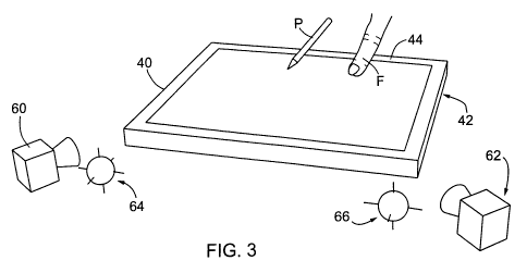
[0019] Figure 3 is a perspective conceptual view of a portion of the
interactive
input system of Figure 1;
[0020] Figure 4 is a schematic diagram of a portion of the interactive input
system of Figure 1;
[0021] Figure 5 shows the on/off timing patterns of image sensors and
infrared light sources during subframe capture.
[0022] Figure 6 is a schematic diagram showing the generation of image
frames by combining different image subframes;
[0023] Figure 7 is a schematic diagram of a modulated lighting controller
shown in Figure 4;
CA 02722820 2010-10-28
WO 2009/135313 PCT/CA2009/000634
-6-
[0024] Figure 8 is a schematic diagram of a subframe controller forming part
of the modulated lighting controller of Figure 7;
[0025] Figure 9 is a schematic diagram of a demodulator forming part of the
modulated lighting controller of Figure 7;
[0026] Figure 10 is a schematic diagram of a light output interface forming
part of the modulated lighting controller of Figure 7.
Detailed Description Of The Embodiments
[0027] Turning now to Figures 1 to 4, an interactive input system that allows
a
user to inject input such as "ink" into an application program is shown and is
generally identified by reference numeral 20. In this embodiment, interactive
input
system 20 comprises an assembly 22 that engages a display unit (not shown)
such as
for example, a plasma television, a liquid crystal display (LCD) device, a
flat panel
display device, a cathode ray tube etc. and surrounds the display surface 24
of the
display unit. The assembly 22 employs machine vision to detect pointers
brought into
proximity with the display surface 24 and communicates with a computer 26
executing one or more application programs via a universal serial bus (USB)
cable 28.
Computer 26 processes the output of the assembly 22 and adjusts image data
that is
output to the display unit so that the image presented on the display surface
24 reflects
pointer activity. In this manner, the assembly 22 and computer 26 allowing
pointer
activity proximate the display surface 24 to be recorded as writing or drawing
or used
to control execution of one or more application programs executed by the
computer
26.
[0028] Assembly 22 comprises a frame assembly that is integral with or
attached to the display unit and surrounds the display surface 24. Frame
assembly
comprises a bezel having three illuminated bezel segments 40 to 44, four
corner
pieces 46 and a tool tray segment 48. Bezel segments 40 and 42 extend along
opposite side edges of the display surface 24 while bezel segment 44 extends
along
the top edge of the display surface 24. The illuminated bezel segments 40 to
44 form
an infrared (IR) light source about the display surface periphery that can be
conditioned to emit infrared illumination so that a pointer positioned within
the region
CA 02722820 2010-10-28
WO 2009/135313 PCT/CA2009/000634
-7-
of interest adjacent the display surface 24 is backlit by the emitted infrared
radiation.
The bezel segments 40 to 44 may be of the type disclosed in U.S. Patent No.
6,972,401 to Akitt et al. and assigned to SMART Technologies ULC of Calgary,
Alberta, Canada, assignee of the subject application, the content of which is
incorporated by reference The tool tray segment 48 extends along the bottom
edge of
the display surface 24 and supports one or more pen tools P. The corner pieces
46
adjacent the top left and top right corners of the display surface 24 couple
the bezel
segments 40 and 42 to the bezel segment 44. The corner pieces 46 adjacent the
bottom left and bottom right corners of the display surface 24 couple the
bezel
segments 40 and 42 to the tool tray segment 48.
[00291 In this embodiment, the corner pieces 46 adjacent the bottom left and
bottom right corners of the display surface 24 accommodate image sensors 60
and 62
that look generally across the entire display surface 24 from different
vantages. The
image sensors 60 and 62 are of the type manufactured by Micron under model No.
MT9V023 and are fitted with an 880nm lens of the type manufactured by Boowon
under model No. BW25B giving the image sensors a 98 degree field of view. Of
course, those of skill in the art will appreciate that other commercial or
custom image
sensors maybe employed. Each corner piece 46 adjacent the bottom left and
bottom
right corners of the display surface 24 also accommodates an IR light source
64, 66
that is positioned proximate to its associated image sensor. The IR light
sources 64
and 66 can be conditioned to emit infrared illumination so that a pointer
positioned
within the region of interest is front lit by the emitted infrared radiation.
[00301 The image sensors 60 and 62 communicate with a modulated lighting
controller 70 that controls operation of the illuminated bezel segments 40 to
44 and
the IR light sources 64 and 66 via light control circuits 72 to 76. Each light
control
circuit 72 to 76 comprises a power transistor and a ballast resistor. Light
control
circuit 72 is associated with the illuminated bezel segments 40 to 44, light
control
circuit 74 is associated with IR light source 64 and light control circuit 76
is
associated with IR light source 66. The power transistors and ballast
resistors of the
light control circuits 72 to 76 act between their associated JR light source
and a power
source. The modulated lighting controller 70 receives clock input from a
crystal
CA 02722820 2010-10-28
WO 2009/135313 PCT/CA2009/000634
-8-
oscillator 78 and communicates with a microprocessor 80. The microprocessor 80
also communicates with the computer 26 over the USB cable 28.
[00311 The modulated lighting controller 70 is preferably implemented on an
integrated circuit such as for example a field programmable gate array (FPGA)
or
application specific integrated circuit (ASIC). Alternatively, the modulated
lighting
controller 70 may be implemented on a generic digital signal processing (DSP)
chip
or other suitable processor.
[00321 The interactive input system 20 is designed to detect a passive pointer
such as for example, a user's finger F, a cylinder or other suitable object as
well as a
pen tool P having a retro-reflective or highly reflective tip, that is brought
into
proximity with the display surface 24 and within the fields of view of the
image
sensors 60 and 62. In general, during operation, the illuminated bezel
segments 40 to
44, the IR light source 64 and the IR light source 66 are each turned on and
off (i.e.
modulated) by the modulated lighting controller 70 in a distinct pattern. The
on/off
switching patterns are selected so that the switching patterns are generally
orthogonal.
As a result, if one switching pattern is cross-correlated with another
switching pattern,
the result is substantially zero and if a switching pattern is cross-
correlated with itself,
the result is a positive gain. This allows image frames to be captured by the
image
sensors 60 and 62 with the illuminated bezel segments 40 to 44 and the IR
light
sources 64 and 66 simultaneously active and the image frames processed to
yield
separate image frames that only include contributions from a selected one of
the IR
light sources.
[0033) In this embodiment, the orthogonal properties of Walsh codes such as
those used in code division multiple access (CDMA) communication systems are
employed to modulate the illuminated bezel segments 40 to 44 and the IR light
sources 64 and 66 thereby to allow the image contributions of different light
sources
to be separated. For example, Walsh codes Wl = {1, -1, 1, -1, 1, -1, 1, -l,}
and W2 =
{1, 1, -1, -1, 1, 1, -1, -1 } are orthogonal meaning that when corresponding
elements
are multiplied together and summed, the result is zero. As will be
appreciated, light
sources cannot take on negative intensities. The illuminated bezel segments 40
to 44,
the JR light source 64 and the IR light source 66 are therefore each turned on
and off
by the modulated lighting controller 70 according to a distinct modified Walsh
code
CA 02722820 2010-10-28
WO 2009/135313 PCT/CA2009/000634
-9-
MW, where a Walsh code bit of value one (1) signifies an on condition and a
Walsh
code bit of value zero (0) signifies an off condition. In particular, the
illuminated
bezel segments 40 to 44 are turned on and off following modified Walsh code
MWl =
{1, 0, 1, 0, 1, 0, 1, 0}. IR light source 64 is turned on and off following
modified
Walsh code MW2 = {1, 1, 0, 0, 1, 1, 0, 0}. IR light source 66 is turned on and
off
following Walsh modified code MW3 = {1, 0, 0, 1, 1, 0, 0, 11. As will be
appreciated,
replacing the negative Walsh code bit values with zero values introduces a dc
bias to
the IR lighting.
[00341 During demodulation, the Walsh codes Wl = {1, -1, 1, -1, 1, -1, 1, -1},
WZ = {1, 1, -1, -1, 1, 1, -1, -1} and W3 = {1, -1, -1, 1, 1, -1, -1, 1} are
employed.
These Walsh codes are of interest as they have spectral nulls at dc, 1201-1z,
2401-1z and
360Hz at a subframe rate of 960Hz. As a result, if these Walsh codes are cross-
correlated, frequencies at dc, 120Hz, 240Hz and 360Hz are eliminated allowing
the
effects of external steady state light (eg. sunlight), the dc bias introduced
by the
modified Walsh codes MWX and the effects of light sources (eg. fluorescent and
incandescent light sources etc.) that flicker at common frequencies i.e. 120Hz
in
North America to be filtered out. If the interactive input system 20 is used
in different
environments where lighting flickers at a different frequency, the subframe
rate is
adjusted to filter out the effects of this flickering light.
[00351 The image sensors 60 and 62 are operated by the modulated lighting
controller 70 synchronously with the on/off switching patterns of the
illuminated
bezel segments 40 to 44, the IR light source 64 and the IR light source 66 so
that eight
(8) subframes at the subframe rate of 960 frames per second (fps) are captured
giving
each image sensor a 120Hz frame rate. Figure 5 shows the on/off switching
patterns
of the IR light sources and the subframe capture rate of the image sensors 60
and 62.
The subframes captured by the image sensors 60 and 62 are combined by the
modulated lighting controller 70 in different combinations to yield a
plurality of
resultant image frames, namely an image frame 90 from each image sensor 60, 62
based substantially only on the contribution of the infrared illumination
emitted by the
illuminated bezel segments 40 to 44, an image frame 92 from image sensor 60
based
substantially only on the contribution of the infrared illumination emitted by
the IR
light source 64, an image frame 94 from image sensor 62 based substantially
only on
CA 02722820 2010-10-28
WO 2009/135313 PCT/CA2009/000634
-10-
the contribution of the infrared illumination emitted by the IR light source
66 and an
image frame 96 from each image sensor 60, 62 based on the contribution of the
infrared illumination emitted by the illuminated bezel segments 40 to 44, the
IR light
source 64, the IR light source 66 and ambient light as shown in Figure 6.
[0036] The resultant image frames generated by the modulated lighting
controller 70 are then conveyed to the microprocessor 80. Upon receipt of the
image
frames, the microprocessor 80 examines the image frames based substantially
only on
the contribution of the infrared illumination emitted by the illuminated bezel
segments
40 to 44 generated for each image sensor 60, 62 to detect the presence of a
pointer.
For these image frames, the illuminated bezel segments 40 to 44 appear as a
bright
band in the image frames. If a pointer is in proximity with the display
surface 24
during capture of the subframes, the pointer will occlude the backlight
infrared
illumination emitted by the illuminated bezel segments 40 to 44. As a result,
the
pointer will appear in each image frame as a dark region interrupting the
bright band.
[0037] The microprocessor 80 processes successive image frames output by
each image sensor 60, 62 in pairs. When a pair of image frames from an image
sensor
is available, the microprocessor 80 subtracts the image frames to form a
difference
image frame and then processes the difference image frame to generate
discontinuity
values representing the likelihood that a pointer exists in the difference
image frame.
When no pointer is proximity with the display surface 24, the discontinuity
values are
high. When a pointer is in proximity with the display surface 24, some of the
discontinuity values fall below a threshold value allowing the existence of
the pointer
in the difference image frame to be readily determined.
[0038] In order to generate the discontinuity values for each difference image
frame, the microprocessor 80 calculates a vertical intensity profile
(VIPbezel) for the
image frame by summing the intensity values of the pixels in each pixel column
of the
image frame. If no pointer exists, the V]Pbezel values will remain high for
all of the
pixel columns of the image frame. However, if a pointer is present in the
image
frame, the VIPbezel values will drop to low values at a region corresponding
to the
location of the pointer in the image frame. The resultant VIPbezel curve
defined by the
VIPbezel values for each image frame is examined to determine if the VIPbezel
curve
CA 02722820 2010-10-28
WO 2009/135313 PCT/CA2009/000634
-11-
falls below a threshold value signifying the existence of a pointer and if so,
to detect
the left and right edges in the VIPbezel curve that represent opposite sides
of a pointer.
[0039] In particular, in order to locate left and right edges in each image
frame, the first derivative of the VIPbezel curve is computed to form a
gradient
curve V VlPbeze](X). If the VIPbe.el curve drops below the threshold value
signifying
the existence of a pointer, the resultant gradient curve V VIPbezel(x) will
include a
region bounded by a positive peak and a negative peak representing the edges
formed
by the dip in the VIPbezel curve. In order to detect the peaks and hence the
boundaries
of the region, the gradient curve V VIPbezel(X) is subjected to an edge
detector.
[0040] In particular, a threshold T is first applied to the gradient curve
V VlPbezel(X) so that, for each position x, if the absolute value of the
gradient curve
V D(x) is less than the threshold, that value of the gradient curve V
VIPbezel(X) is set
to zero as expressed by:
V VIPbezel(X) = 0, if I V VIPbezet(x)I < T
[0041] Following the thresholding procedure, the thresholded gradient curve
V VIPbezel(x) contains a negative spike and a positive spike corresponding to
the left
edge and the right edge representing the opposite sides of the pointer, and is
zero
elsewhere. The left and right edges, respectively, are then detected from the
two non-
zero spikes of the thresholded gradient curve V VlPbeze](X). To calculate the
left edge,
the centroid distance CDleft is calculated from the left spike of the
thresholded
gradient curve V VIPbezel(x) starting from the pixel column Xleft according
to:
I (xi - X left )VVIPbezel (xi )
CDleft -
V VIPbezel (xi )
where x; is the pixel column number of the i-th pixel column in the left spike
of the
gradient curve V VIPbezel(X), i is iterated from 1 to the width of the left
spike of the
thresholded gradient curve V VIPbezei(X) and X1eft is the pixel column
associated with a
value along the gradient curve V VIPbezel(x) whose value differs from zero (0)
by a
threshold value determined empirically based in system noise. The left edge in
the
thresholded gradient curve V VIPbezel(x) is then determined to be equal to
Xleft + CDleft.
CA 02722820 2010-10-28
WO 2009/135313 PCT/CA2009/000634
-12-
[0042] To calculate the right edge, the centroid distance CDright is
calculated
from the right spike of the thresholded gradient curve V VIPbezel(x) starting
from the
pixel column X,;ght according to:
I (xi - X right )VVIPbeze1 (xj )
CDpght
VVIPbezel(xi)
where xj is the pixel column number of the j-th pixel column in the right
spike of the
thresholded gradient curve V VIPbezel(x), j is iterated from 1 to the width of
the right
spike of the thresholded gradient curve V VlPbezel(x) and Xright is the pixel
column
associated with a value along the gradient curve V VIPbezel(x) whose value
differs from
zero (0) by a threshold value determined empirically based on system noise.
The right
edge in the thresholded gradient curve is then determined to be equal to
Xright + CDright.
[0043] Once the left and right edges of the thresholded gradient curve
V VIPbezei(x) are calculated, the midpoint between the identified left and
right edges is
then calculated thereby to determine the location of the pointer in the
difference
image frame.
[0044] If a pointer is detected in the image frames based substantially only
on
the contribution of the infrared illumination emitted by the illuminated
bezels 40 to
44, image frames based substantially only on the contribution of infrared
illumination
emitted by the IR light source 64 and image frames based substantially only on
the
contribution of infrared illumination emitted by the IR light source 66 are
processed
to determine if the pointer is a pen tool P. As will be appreciated, if the
pointer is a
pen tool P, the pen tool P will appear as a bright region on a dark background
in the
image frames captured by each image sensor due to the reflection of emitted
infrared
illumination by the retro-reflective pen tool tip back towards the IR light
sources and
hence, towards the image sensors 60 and 62. If the pointer is a finger F, then
the
pointer will appear substantially darker in at least one of these image
frames.
[0045] If the existence of a pen tool P is determined, the image frames, are
processed in the same manner described above in order to determine the
location of
the pen tool P in the image frames.
[0046] After the location of the pointer in the image frames has been
determined, the microprocessor 80 uses the pointer positions in the image
frames to
CA 02722820 2010-10-28
WO 2009/135313 PCT/CA2009/000634
-13-
calculate the position of the pointer in (x,y) coordinates relative to the
display surface
24 using triangulation in the well known manner such as that described in
above-
incorporated U.S. Patent No. 6,803,906 to Morrison et al. The calculated
pointer
coordinate is then conveyed by the microprocessor 80 to the computer 26 via
the USB
cable 28. The computer 26 in turn processes the received pointer coordinate
and
updates the image output provided to the display unit, if required, so that
the image
presented on the display surface 24 reflects the pointer activity. In this
manner,
pointer interaction with the display surface 24 can be recorded as writing or
drawing
or used to control execution of one or more application programs running on
the
computer 26.
[00471 The components of the modulated lighting controller 70 and its
operation will now be described with particular reference to Figures 7 to 10.
Turning
now to Figure 7, the modulated lighting controller 70 is better illustrated.
As can be
seen, the modulated lighting controller 70 comprises an image sensor
controller 100
that receives the clock signals output by the crystal oscillator 78. The image
sensor
controller 100 provides timing signals to the image sensors 60 and 62 to set
the image
sensor subframe rates and is connected to a subframe controller 102 via
PIXCLK,
LED, Frame_Valid and Line_Valid signal lines. The image sensor controller 100
also
communicates with a plurality of demodulators, in this case six (6)
demodulators 104a
to 104f. In particular, the image sensor controller 100 is connected to
demodulators
104a to 104c via a CAM1DATA line and is connected to demodulators 104d to 104f
via a CAM2DATA line. The image sensor controller 100 is also connected to the
demodulators 104a to 104f via the PIXCLK signal line. The demodulators 104a to
104f are connected to an output interface 106 via D, A and OEX signal lines.
The
output interface 106 is also connected to the subframe controller 102 via line
108, to
the image sensor controller 100 via the PIXCLK signal line and to the
microprocessor
80.
[00481 The subframe controller 102 is connected to each of the demodulators
104a to 104f via subframe D, EN and address signal lines. The subframe
controller
102 is also connected to each of the light control interfaces 110 to 114 via
subframe_L and EXP signal lines. The light control interfaces 110 to 114 are
also
connected to the PIXCLK signal line. Light control interface 110 is connected
to the
CA 02722820 2010-10-28
WO 2009/135313 PCT/CA2009/000634
-14-
light control circuit 72, light control interface 112 is connected to the
light control
circuit 74 and light control interface 114 is connected to light control
circuit 76.
[0049] Figure 8 better illustrates the subframe controller 102. As can be
seen,
the subframe controller 102 comprises four input terminals 150 to 156 that
receive the
LED, Frame_Valid, PIXCLK and Line Valid signal lines extending from the image
sensor controller 100. In particular, input terminal 150 receives the LED
signal line,
input terminal 152 receives the PIXCLK signal line, input terminal 154
receives the
Frame_Valid signal line and input terminal 156 receives the Line_Valid signal
line.
The subframe controller 102 also comprises six output terminals, namely an EXP
output terminal 160, a subframe_L output terminal 162, a subframe D output
terminal
164, an INT output terminal 166, an address output terminal 168 and an EN
output
terminal 170. A three-bit counter 180 has its input connected to the LED input
terminal 150 and its output connected to the subframe_L output terminal 162.
The
input of a latch 182 is also connected to the LED input terminal 150. The
output of
the latch 182 is coupled to the EXP output terminal 160. The control input of
the
latch 182 is connected to the PIXCLK input terminal 152. The PIXCLK input
terminal 152 is also connected to the control input of a pair of latches 184
and 186
and to the control input of a counter 188. The D input of latch 184 is
connected to the
zero input of the counter 188 through an inverter 190. The Q input of latch
184 is
connected to the inverting input of a gate 192 and to the D input of the latch
186. The
Q input of latch 186 is connected to the non-inverting input of the gate 192.
The
output of the gate 192 is connected to one input of a gate 194. The other
input of the
gate 194 is connected to the output of a comparator 196. The output of the
gate 194 is
connected to the INT output terminal 166.
[0050] The control input of a latch 200 is also connected to the LED input
terminal 150. The D input of the latch 200 is connected to the subframe_L
output
terminal 162. The Q input of the latch 200 is connected to the D input of a
latch 202.
The control input of the latch 202 is connected to the Frame_Valid input
terminal 154
while its Q input is connected to the subframe_D output terminal 164 and to
the input
of the comparator 196. The EN input of the counter 188 is connected to the
Line_Valid input terminal 156 while the output pin of the counter 188 is
connected to
CA 02722820 2010-10-28
WO 2009/135313 PCT/CA2009/000634
-15-
the address output terminal 168. The Line_Valid input terminal 156 is also
connected
directly to the EN output terminal 170.
[0051] Figure 9 better illustrates one of the demodulators 104a to 104f. As
can be seen, the demodulator comprises seven (7) input terminals 210, namely a
subframe input terminal, a data input terminal 212, an EN input terminal 214,
a
PIXCLK input terminal 216, an address input terminal 218, an OE input terminal
220
and an A input terminal 222. The demodulator also comprises a single D output
terminal 224. A latch 230 has its input connected to the data input terminal
and its
output connected to the input of an expander unit 232. The control input of
the latch
230 is connected to the PIXCLK input terminal 216. The output of the expander
unit
232 is connected to the B input of an algebraic add/subtract unit 234. The A
input of
the algebraic unit 234 is connected to the output of a multiplexer 236. The
output of
the algebraic unit 234 is connected to the DA input of a working buffer 240 in
the
form of a two-part memory unit. One input of the multiplexer 236 is connected
to a
null input 242 and the other input pin of the multiplexer 236 is connected to
a line 244
extending between the DB input of the working buffer 240 and the DA input of
an
output buffer 250 in the form of a two-part memory unit. The control input of
the
multiplexer 236 is connected to a line 252 extending between the output of a
comparator 254 and one input of a gate 256. The input of the comparator 254
and the
input of a lookup table 258 are connected to the subframe input terminal 210.
The
output of the lookup table 258 is connected to the control input of the
algebraic unit
234. A logic one (1) in the lookup table 258 indicates a Walsh code bit value
of"1"
and instructs the algebraic unit 234 to perform the add operation. A logic
zero (0) in
the lookup table 258 indicates a Walsh code bit value of "-1" and instructs
the
algebraic unit 234 to perform the subtract operation. In this example, the
lookup table
258 is programmed with Walsh code W1: {} to enable illumination
from the bezel segments 40 to 44 to be demodulated, Walsh code W2: {1,1,-1,-
1,1,1,-
1,-1} to enable illumination from IR light source 64 to be demodulated and
Walsh
code W3: {1,-1,-1,1,1,-1,-1,1} to enable illumination from IR light source 66
demodulated. To enable image frames to be captured that are based on the
contribution of all emitted infrared illumination including ambient light, the
lookup
table 250 is programmed with Walsh code Wo: {1,1,1,1,1,1,1,1}.
CA 02722820 2010-10-28
WO 2009/135313 PCT/CA2009/000634
-16-
[00521 The other input of the gate 256 is connected to a line 260 extending
between the output of a latch 262 and the WEA input of the working buffer 240.
The
output of the gate 256 is connected to the WEA input of the output buffer 250.
The
input of the latch 262 is connected to the EN input terminal 214 and the
control input
of the latch 262 is connected to the PIXCLK input terminal 216. The PIXCLK
input
terminal 216 is also connected to the control inputs of the working and output
buffers
240 and 250 respectively as well as to the control input of a latch 264. The
input of
the latch 264 is connected to the address input terminal 218. The output of
the latch
264 is connected to the AA inputs of the working and output buffers 240 and
250
respectively. The address input terminal 218 is also connected to the AB input
of the
working buffer 240. The OEB and AB inputs of the output buffer 250 are
connected to
the OE and A input terminals 220 and 222 respectively.
[00531 Figure 10 better illustrates one of the light control interfaces 110 to
114. As can be seen, the light control interface comprises an SF input
terminal 280,
an EXP input terminal 282 and a CLK input terminal 284. The light control
interface
also comprises a single output terminal 286. The input of an 8x1 lookup table
290 is
connected to the SF input terminal 280. The output of the lookup table 290 is
connected to one input of a gate 292. The second input of the gate 292 is
connected
to the EXP input terminal 282 and the third input of the gate 292 is connected
to the Q
input of a pulse generator 294. The T input of the pulse generator 294 is
connected to
the EXP input terminal 282 and the control input of the pulse generator 294 is
connect
to the CLK input terminal 284. The output of the gate 292 is connected to the
output
terminal 286. The lookup table 290 stores the state of the Walsh code for each
subframe that determines the on/off condition of the associated JR light
source during
capture of that subframe. Thus, for the illuminated bezel segments 40 to 44,
the
lookup table 290 of light control interface 110 is programmed with modified
Walsh
code MWl = {1,0,1,0,1,0,1,0}. For IR light source 64, the lookup table 290 of
light
control interface 112 is programmed with modified Walsh code MW2 =
{1,1,0,0,1,1,0,0}. For IR light source 66, the lookup table 290 of the light
control
interface 114 is programmed with modified Walsh code MW3 = {1,0,0,1,1,0,0,1}.
[00541 In terms of operation, the demodulators 104a and 104d are
programmed to output the image frames from image sensors 60 and 62 that are
based
CA 02722820 2010-10-28
WO 2009/135313 PCT/CA2009/000634
-17-
substantially only on infrared illumination emitted by the bezel segments 40
to 44.
The demodulator 104b is programmed to output the image frame from image sensor
60 based substantially only on infrared illumination emitted by IR light
source 64 and
the demodulator 104e is programmed to output the image frame from image sensor
62
based substantially only on infrared illumination emitted by IR light source
66. The
demodulators 104c and 104f are programmed to output the image frames from
image
sensors 60 and 62 that are based on the infrared illumination emitted by all
of the IR
light sources as well as ambient light. These image frames give the
microprocessor
80 an unmodulated view of the region of interest allowing the microprocessor
to
perform exposure control of the image sensors and possibly further object
classification.
[0055] The light output interfaces 110 to 114 provide output signals to their
associated IR light sources following the assigned modified Walsh code MWX. As
mentioned previously, the Walsh codes are synchronized to the exposure times
of the
image sensors 60 and 62.
[0056] The image sensor controller 100 provides the control signals to and
collects the image subframes from each of the image sensors 60 and 62. The
clock
signal from the crystal oscillator 78 is used to generate the clock signals
for both
image sensors. The image sensors 60 and 62 are driven so that they expose
their
image subframes at the same time and deliver the subframe data at the same
time.
The image sensors in this embodiment provide the subframe data on the CAMIDATA
and CAM2DATA data lines respectively, a pixel clock signal on the PIXCLK
signal
line, a signal that indicates that a subframe is being exposed on the LED
signal line, a
signal that indicates that a subframe is being clocked out on the FRAME VALID
signal line, and a signal that indicates that the data lines have valid pixel
information
on the LINE VALID signal line. The image sensors have a 12-bit resolution (0
to
4095) which is compressed into a 10-bit word (0 to 1023) using a non-linear
function
or other suitable compression method. The 10-bit data lines are uncompressed
prior
to demodulation in order to inhibit the resulting non-linear function from
destroying
the properties of the Walsh codes.
[0057] The output interface 106 provides the necessary signals to get the
resultant image frames to the microprocessor 80. The form of the output
interface is
CA 02722820 2010-10-28
WO 2009/135313 PCT/CA2009/000634
-18-
dependent on the type of microprocessor employed and the transfer mode chosen.
The internal signal on the INT line is generated by the subframe controller
102 when
a new subframe is available in the demodulators 104a to 104f. The output
interface
106 enables the output of the first demodulator 104a through the OE1 signal
line. The
output interface 106 then sequences through the addresses (A) and reads the
data (D)
for each pixel, serializes the result, and sends the result to the
microprocessor 80. The
process is then repeated for the five other demodulators 104b to 104f using
the five
remaining output enable lines OE2 to OE6 until all of the pixel information is
transmitted to the microprocessor 80.
[0058] The subframe controller 102 is tasked with maintaining
synchronization and subframe count. The 3-bit counter 180 outputs the subframe
number (0-7) that is currently being exposed by the image sensors 60 and 62 to
the
light output interfaces 110 to 114 via the subframe_L line. The counter 180 is
incremented at the start of every image sensor exposure by the signal on the
LED line
and wraps around to zero after the last subframe. The data from the image
sensors 60
and 62 is not clocked out until sometime after the end of the exposure (the
falling
edge of LED signal). Latches 300 and 202 delay the subframe count to the next
positive edge of the FRAME VALID signal and this information is sent to the
demodulators 104a to 104f to indicate which subframe they are currently
processing.
The EXP signal is output to the light output interfaces 110 to 114 to allow
them to
turn their associated IR light sources on. The EXP signal is delayed slightly
by latch
182 to ensure that the subframe_L signal line is stable when the IR light
sources are
activated.
[0059] Within each subframe, counter 188 provides a unique address for each
pixel. The counter is zeroed at the start of each subframe and incremented
whenever
a valid pixel is read in. This address is sent to each of the demodulators
104a to 104f
along with an enable (EN) that indicates when the CAMIDATA and CAM2DATA
data lines are valid.
[0060] Valid data is available from the demodulators 104a to 104f at the end
of every subframe 0. Latches 184 and 186 and gate 192 provide a single
positive
pulse at the end of every FRAME_VALID signal. Comparator 196 and gate 194
allow this positive pulse to pass only at the end of subframe 0. This provides
the
CA 02722820 2010-10-28
WO 2009/135313 PCT/CA2009/000634
-19-
signal on the INT signal line to the output interface 106 indicating that a
new resultant
image frame is ready to send.
[00611 The working buffer 240 is used to store intermediate image frames.
New pixels are added or subtracted from the working buffer 240 using the
algebraic
unit 234 according to the selected Walsh code stored in the lookup table 258.
[00621 During subframe 0, image sensor data is transferred directly into the
working memory 240. Comparator 254 outputs a logic 1 during subframe 0 which
forces multiplexer 236 to force a zero onto the A input of the algebraic unit
234. The
output of the lookup table 258 is always a logic 1 during subframe 0 and
therefore, the
algebraic unit 234 will always add input B to input A (zero), effectively
copying input
B into the working buffer 240. At each PIXCLK positive edge, the raw data from
the
image sensor is latched into latch 230, its address is latched into latch 264,
and its
valid state (EN) is latched into latch 262. As noted above, the data from the
image
sensor is in a compressed 10-bit form that must be expanded to its original
linear 12-
bit form before processing. This is done by the expander unit 232. The
expander unit
232 also adds an extra three high-order bits to create a 15-bit signed format
that
inhibits underflow or overflow errors during processing. If the data is valid
(output of
latch 262 is high) then the expanded data will pass through the algebraic unit
234
unmodified and be latched into the working buffer 240 through its DA input at
the
pixel address AA. At the end of subframe 0, the entire first subframe is
latched into
the working buffer 240.
[00631 The pixel data in the remaining subframes (1-7) must be either added
to or subtracted from the corresponding pixel values in the working buffer
240.
While the DATA, ADDRESS, and EN signals are being latched in latches 230, 264,
and 262, the current working value of that pixel is latched into the DB input
of the
working buffer 240. Comparator 254 goes to logic zero in these subframes which
causes multiplexer 236 to put the current working value of the pixel to the A
input of
the algebraic unit 234. The lookup table 258 determines whether the new image
data
at input B should be added to or subtracted from the current working value
according
to the Walsh code, where a Walsh code bit of value one (1) represents the add
operation and a Walsh code bit of value zero (0) represents the subtract
operation.
CA 02722820 2010-10-28
WO 2009/135313 PCT/CA2009/000634
-20-
The result is then put back into the same address in the working buffer 240 in
the next
clock cycle through the DA input.
[0064] After processing all eight subframes, the working buffer 240 contains
the final resultant image frame. During subframe 0 of the following subframe,
this
resultant image frame is transferred to the output buffer 250. Since subframe
0 does
not use the output from the DB input of working buffer 240, this same port is
used to
transfer the resultant image frame to the output buffer 250. Gate 256 enables
the
write-enable input of the A-port (WEA) of the ouput buffer 250 during subframe
zero.
The data from the working buffer 240 is then transferred to the output buffer
250 just
before being overwritten by the next incoming subframe. The DB, address and
output
enable OB lines of the output buffer 250 are then used to transfer the
resultant image
frame through the output interface 106 to the microprocessor 80.
[0065] Just before the exposure signal (EXP) goes high, the subframe
controller 102 sets the current subframe that is being exposed (SF). If the
lookup
table 290 outputs a zero (0), then gate 292 keeps the associated IR light
source off for
this subframe. If the lookup table outputs a one (1), then the associated IR
light
source is switched on. The on duration is determined by the pulse generator
294. The
pulse generator 294 starting with trigger (T), outputs a positive pulse a
given number
of clock cycles (in this case the pixel clock) long. At the end of the pulse,
or when the
image sensor exposure time is done, the gate 292 switches off the associated
IR light
source.
[0066] The pulse generators 294 allow the influence of each IR light source to
be dynamically adjusted independently of the other light sources and of the
sensor
integration time to get the desired balance. With the pulse time in each IR
light
source held constant, the exposure time of the image sensors 60 and 62 can be
adjusted to get the best ambient light images (demodulators 104c and 104f)
without
affecting the modulated image frames (demodulators 104a, 104b, 104d, and
104e).
The smallest possible integration time of the image sensors is equal to the
longest
pulse time of the three IR light sources. The largest possible integration
time of the
image sensors is the point where the pixels start to saturate, in which case
the
demodulation scheme will experience a failure.
CA 02722820 2010-10-28
WO 2009/135313 PCT/CA2009/000634
-21-
[0067] In the embodiment described above, Walsh codes are employed to
modulate and demodulate the IR light sources. Those of skill in the art will
appreciate
that other digital codes may be employed to modulate and demodulate the IR
light
sources such as for example, those used in OOK, FSK, ASK, PSK, QAM, MSK,
CPM, PPM, TCM, OFDM, FHSS or DSSS communication systems.
[0068] Although the image sensors are shown as being positioned adjacent the
bottom corners of the display surface, those of skill in the art will
appreciate that the
image sensors may be located at different positions relative to the display
surface.
The tool tray segment need not be included and if desired may be replaced with
an
illuminated bezel segment. Also, although the illuminated bezel segments 40 to
44
and light sources 64 and 66 are described as IR light sources, those of skill
in the art
will appreciate that other suitable radiation sources may be employed.
[0069] Although the interactive input system 20 is described as detecting a
pen tool having a retro-reflective or highly reflective tip, those of skill in
the art will
appreciate that the interactive input system can also detect active pointers
that emit
signals when in proximity to the display surface 24. For example, the
interactive
input system may detect active pen tools that emit infrared radiation such as
that
described in U.S. Patent Application Serial No. 12/118,535 to Bolt et al.
entitled
"Interactive Input System And Pen Tool Therefor" filed on May 9, 2008 and
assigned
to SMART Technologies ULC of Calgary, Alberta, the content of which is
incorporated by reference.
[0070] In this embodiment, when an active pen tool is brought into proximity
with the display surface 24, the active pen tool emits a modulated signal
having
components at frequencies equal to 120Hz, 240Hz and 360Hz. These frequencies
are
selected as the Walsh codes have spectral nulls at these frequencies. As a
result, the
modulated light output by the active pen tool is filtered out during
processing to detect
the existence of the active pen tool in the region of interest and therefore,
does not
impact pointer detection. When the existence of a pointer is detected, the
microprocessor 80 subjects the image frame based on the infrared illumination
emitted by all of the IR light sources as well as ambient light, to a Fourier
transform
resulting in the dc bias and the 480Hz component of the image frame
representing the
contribution from the illuminated bezel segments being removed. The
CA 02722820 2010-10-28
WO 2009/135313 PCT/CA2009/000634
-22-
microprocessor 80 then examines the resulting image frame to determine if any
significant component of the resulting image frame at 120Hz, 240Hz and 360Hz
exists. If so, the signal pattern at these frequencies is used by the
microprocessor 80
to identify the active pen tool.
[0071] As will be appreciated, as the modulated signal emitted by the active
pen tool can be used by the microprocessor 80 to identify the active pen tool,
detection of multiple active pen tools in proximity of the display surface 24
is
facilitated. If during pointer detection, two or more dark regions
interrupting the
bright band are detected, the modulated light output by the active pen tools
can be
processed separately to determine if the modulated signal components at
frequencies
equal to 120Hz, 240Hz and 360Hz thereby to allow the individual active pen
tools to
be identified. This inhibits modulated signals output by the active pen tools
from
interfering with one another and enables each active pen tool to be associated
with the
image presented on the display surface 24 allowing active pen tool input to be
processed correctly.
[0072] The interactive input system may of course take other forms. For
example, the illuminated bezel segments may be replaced with retro-reflective
or
highly reflective bezels as described in the above-incorporated Bolt et al.
application.
Those of skill in the art will however appreciate that the radiation
modulating
technique may be applied to basically any interaction input system that
comprises
multiple radiation sources to reduce interference and allow information
associated
with each radiation source to be separated.
[0073] Although embodiments have been described with reference to the
drawings, those of skill in the art will appreciate that variations and
modifications
may be made without departing from the spirit and scope thereof as defined by
the
appended claims.