Note: Descriptions are shown in the official language in which they were submitted.
CA 02722942 2010-10-28
WO 2009/137578 PCT/US2009/042983
[0001] TITLE
SEMICONDUCTOR DEVICES WITH NON-PUNCH-THROUGH
SEMICONDUCTOR CHANNELS HAVING ENHANCED CONDUCTION AND
METHODS OF MAKING
[0002] The section headings used herein are for organizational purposes only
and should
not be construed as limiting the subject matter described herein in any way.
[0003] BACKGROUND
[0004] Field
[0005] This application relates generally to semiconductor devices and to
methods of
making the devices.
[0006] Background of the Technolory
[0007] In junction field-effect devices used in power switching applications,
it is often
highly desirable to not only reduce the channel resistance but also provide a
MOSFET-
like switching behavior. In particular, once the channel is pinched-off by the
threshold
voltage applied to the gate, it would be desirable if the device can block the
maximum or
rated voltage. Such device property requires infinitely high voltage blocking
gain R. In
junction field-effect devices, low channel resistance and high voltage
blocking gain are
typically viewed as competing device characteristics. For example, in short-
channel
JFETs or SITs, the channel component of the total device resistance is
relatively small
and current saturation is much less pronounced than in longer channel JFET
structures.
However, the voltage-blocking gain is also small and the difference between
the threshold
voltage and the gate bias required to block the maximum drain voltage is very
significant,
reaching in some cases tens of volts (e.g., Merrett et al. [1]). On the other
hand, in long
channel enhancement-mode JFETs that can provide high voltage-blocking gain,
the
1
CA 02722942 2010-10-28
WO 2009/137578 PCT/US2009/042983
current saturates too early to fully utilize relatively low on-state channel
resistance in the
linear region (e.g., Zhao et al. [2] and Sannuti et al. [3]). This problem is
especially
pronounced in the case of power SiC VJFETs. As a result, the development of
normally-
off switching devices has been impaired.
[0008] Accordingly, there still exists a need for junction field-effect
semiconductor
devices having low on-state channel resistance and high voltage-blocking gain.
[0009] SUMMARY
[0010] A semiconductor device is provided which comprises:
a substrate layer of a semiconductor material of a first conductivity type;
a first layer of a semiconductor material of the first conductivity type on
the
substrate layer;
a raised region of a semiconductor material of the first conductivity type on
the
first layer, the raised region comprising an upper surface and first and
second tapered
sidewalls;
semiconductor material of a second conductivity type different than the first
conductivity type on the first and second sidewalls of the raised region and
on the upper
surface of the first layer adjacent to the raised region; and
a third layer of a semiconductor material of the first conductivity type on
the
upper surface of the raised region;
wherein the raised region comprises a first portion with a first average
dopant
concentration adjacent the third layer and a second portion with a second
average dopant
concentration between the first portion and the first layer, wherein the first
average
dopant concentration is lower than the second average dopant concentration and
wherein
2
CA 02722942 2010-10-28
WO 2009/137578 PCT/US2009/042983
the second average dopant concentration is higher than the average dopant
concentration
of the first layer.
[0011] A circuit comprising one or more semiconductor devices as set forth
above is also
provided.
[0012] A method of making a semiconductor device is also provided which
comprises:
selectively etching through a third layer of a semiconductor material of a
first
conductivity type, wherein the third layer is on a second layer of a
semiconductor
material of the first conductivity type and wherein the second layer is on a
first layer of a
semiconductor material of the first conductivity type and wherein the first
layer is on a
substrate layer of a semiconductor material of the first conductivity type,
wherein
selectively etching through the third layer comprises selectively etching into
the
underlying second layer to form a raised region of semiconductor material of
the first
conductivity type having an upper surface comprising semiconductor material of
the third
layer and tapered sidewalls comprising semiconductor material of the second
layer;
selectively implanting dopants into the semiconductor material of the second
layer
on the sidewalls of the raised region to form regions of semiconductor
material of a
second conductivity type different than the first conductivity type on the
sidewalls of the
raised region and on the upper surface of the first layer adjacent to the
raised region;
wherein the second layer comprises a first portion with a first average dopant
concentration adjacent the third layer and a second portion with a second
average dopant
concentration between the first portion and the first layer, wherein the first
average
dopant concentration is lower than the second average dopant concentration and
wherein
the second average dopant concentration is higher than the average dopant
concentration
of the first layer.
3
CA 02722942 2010-10-28
WO 2009/137578 PCT/US2009/042983
[0013] These and other features of the present teachings are set forth herein.
[0014] BRIEF DESCRIPTION OF THE DRAWINGS
[0015] The skilled artisan will understand that the drawings, described below,
are for
illustration purposes only. The drawings are not intended to limit the scope
of the present
teachings in any way.
[0016] FIG. 1 is a schematic cross-section of a SiC VJFET structure with a non-
punch
through (NPT) channel having reduced resistance.
[0017] FIG. 2 is a schematic illustrating various exemplary doping profiles in
a non-
uniformly doped non-punch through (NPT) channel.
[0018] FIG. 3A is a schematic illustrating various exemplary doping profiles
in a non-
uniformly doped non-punch through (NPT) channel having a gradually doped field
suppressing layer.
[0019] FIG. 3B is a schematic illustrating various exemplary doping profiles
in a non-
uniformly doped non-punch through (NPT) channel having a stepwise doped field
suppressing layer.
[0020] FIG. 4 is a graph showing overlaid measured and simulated I-V
characteristics of
a 1 mm2 normally-off 1500 V 4H-SiC VJFET device with a channel having uniform
doping concentration of 5 x 10¹⁶ CM -3 and rectifying junctions formed using
zero-degree
ion-implantation.
[0021] FIG. 5A is a graph showing simulated I-V characteristics for a 1 mm2
normally-
off 800 V SiC VJFET with rectifying junctions formed using zero-degree ion-
implantation having uniform channel doping.
4
CA 02722942 2010-10-28
WO 2009/137578 PCT/US2009/042983
[0022] FIG. 5B is a pie chart showing the components of the total resistance
for a 1 mm2
normally-off 800 V SiC VJFET with rectifying junctions formed using zero-
degree ion-
implantation having uniform channel doping.
[0023] FIG. 6A is a graph showing simulated I-V characteristics for a 1 mm2
normally-
off 800 V SiC VJFET with rectifying junctions formed using zero-degree ion-
implantation having non-uniform channel doping.
[0024] FIG. 6B is a pie chart showing the components of the total resistance
for a 1 mm2
normally-off 800 V SiC VJFET with rectifying junctions formed using zero-
degree ion-
implantation having non-uniform channel doping.
[0025] DESCRIPTION OF THE VARIOUS EMBODIMENTS
[0026] For the purposes of interpreting this specification, the use of "or"
herein means
"and/or" unless stated otherwise or where the use of "and/or" is clearly
inappropriate.
The use of "a" herein means "one or more" unless stated otherwise or where the
use of
one or more" is clearly inappropriate. The use of "comprise, " "comprises, "
"comprising, " "include, " "includes, " and "including" are interchangeable
and not
intended to be limiting. Furthermore, where the description of one or more
embodiments
uses the term "comprising, " those skilled in the art would understand that,
in some
specific instances, the embodiment or embodiments can be alternatively
described using
the language "consisting essentially of" and/or "consisting of. " It should
also be
understood that in some embodiments the order of steps or order for performing
certain
actions is immaterial so long as the present teachings remain operable.
Moreover, in
some embodiments two or more steps or actions can be conducted simultaneously.
[0027] High channel resistance and low voltage-blocking gain have been treated
in the
past as separate problems. The channel resistance is a non-linear function of
the biases
applied to the channel terminals and to the rectifying junctions. Two regions
can be
conditionally distinguished in the I-V characteristics of the channel where
the channel
CA 02722942 2010-10-28
WO 2009/137578 PCT/US2009/042983
resistance is almost constant: the linear region and the saturation region. In
the linear
region, the channel resistance is proportional to the channel length and
inversely
proportional to the doping concentration and the cross-sectional area of the
current pass.
In the saturation region, the channel resistance grows drastically, making
this region of
little use in most power switching applications.
[0028] The mechanism of current saturation in junction field-effect
transistors was
disclosed in Shockley [4]. This effect can be described as follows. As the
drain-source
bias applied to a JFET structure increases at a fixed gate-source bias, the
potential drop in
the channel along the current flow causes the depletion region inside the
channel to widen
toward the drain. Because of this, the current path inside the channel becomes
narrower
toward the drain, causing the current to saturate. The mechanism described in
Shockley
later appeared to be even more severe due to saturation of carrier drift
velocity at high
electric fields. According to Ohm's law, as the channel resistivity increases
toward the
drain, the electric field also increases resulting in carrier mobility
degradation, which
causes a further increase in the channel resistivity and even faster
saturation of the drain
current.
[0029] Several approaches to solve the problem of early current saturation
have been
proposed. U.S. Patent No. 2,984,752, for example, discloses a channel
structure that
reduces the effect of current saturation utilizing non-uniform spacing between
alloyed p-n
junctions. The distance between the junctions linearly increases toward the
terminal with
the higher bias resulting in the higher current that can be driven through the
channel
before its pinch-off by the merging space-charge regions. The device structure
disclosed
in U.S. Patent No. 2,984,752 is extremely difficult to manufacture, however,
due to the
alloyed junctions.
6
CA 02722942 2010-10-28
WO 2009/137578 PCT/US2009/042983
[0030] The device disclosed in U.S. Patent No. 2,984,752 is also not suitable
for high-
voltage applications because it does not have a voltage blocking layer (i.e.,
a drift region)
between the channel and the drain. The resistance of a drift region could be
minimized
for the targeted breakdown voltage Vb and maximum allowed plain junction
electric field
EIDMAX by choosing the doping Ndr and thickness tdr as set forth in the
following equation:
3 Vb
tdr =
2 EIDMAX
2 M.
4 E o = r EJDMAX
Ndr=-.
9 q Vb
[0031] A device having a vertical channel structure which is formed by plasma
etching
and confined by implanted rectifying junctions is disclosed in U.S. Patent No.
4,403,396.
[0032] A vertical SiC JFET that has a drift region and wherein the saturation
current is
improved using non-uniform spacing between the junctions is disclosed in U.S.
Patent
No. 5,747,831. Although this device can be more easily manufactured than the
structure
disclosed in U.S. Patent No. 2,984,752, the vertical SiC JFET disclosed in
U.S. Patent
No. 5,747,831 is not suited for high-voltage devices that exhibit MOSFET-like
switching
behavior (i.e., infinitely high blocking gain) as explained below.
[0033] Infinitely high blocking gain is represented by the equation:
dVDS ->-~ at VGS <Vh.
dVGS
A hypothetical channel of length L where the current flows between the source
(y = 0)
and the drain (y = L) entrances and is confined by rectifying junctions (e.g.,
p-n junctions)
which are symmetrical with respect to the channel axis can be considered. If
the doping
concentration along the channel axis as defined by N(y) and a(y) represents
the half-
7
CA 02722942 2010-10-28
WO 2009/137578 PCT/US2009/042983
distance between the rectifying junctions, the pinch-off voltage can be
defined along the
channel axis as follows:
Vp(y)=gN(y)2) ye[0,L] (2).
[0034] The following non-punch-through (NPT) conditions, where Vbi (y) is
built-in
potential, and Em stands for the maximum electric field that occurs at the
drain entrance
of the channel when the maximum drain voltage (Vs = Vb) is applied can then be
set
along the channel axis :
Vpunch-through (.Y)-nth+Vbi(.Y)>_Yp(p), .y[0,L] (3)
L
4
Epunch-through = q f N(y)dy > E. O
0
[0035] In the case of a device structure having a drift region optimized for
the lowest
resistance, targeted breakdown voltage (Vb) and maximum allowed plain junction
electric
field EIDMax using equation (1), the conditions (3) - (4) can be rewritten as
the following
set of constraints:
Lv L
if f N(~)d~dy+ f N(y)dy > ElDM.4x
tar 00 0 q
(5)
a(y)< V~N d~d A + N (Vbi(y)-Vh)1Y [0,L]
) q (y)
[0036] For the case of uniform channel doping concentration, the set of
constraints (5)
can be simplified as follows:
8
CA 02722942 2010-10-28
WO 2009/137578 PCT/US2009/042983
L>tdY I11+3N_1
NCh
(6)
a(y)e Y2+ 2 (Vbi-Vh), ye[O,L]
gNCh
[0037] Since the vertical SiC JFET disclosed in U.S. Patent No. 5,747,831 has
channel
and drift regions with the same doping concentration (Ndr = Nh), if the
conditions (6) are
satisfied, the channel length in this structure would exceed the drift region
thickness (L >
tdr). This would be impractical for high-voltage devices that require
relatively thick low
doped drift regions.
[0038] A vertical SiC Static Induction Transistor (SIT) structure having
higher doping
concentrations in the channel layer than in the drift region is disclosed in
U.S. Patent No.
5,945,701.
[0039] A static induction transistor (SIT) structure where the channel
consists of a layer
with "low" impurity concentration separated from the source with a layer with
"very low"
impurity concentration is disclosed in U.S. Patent No. 4,364,072.
[0040] U.S. Patent Application Publication No. 2007/0187715 Al discloses a
device
having a uniformly doped channel structure that can provide non-punch-through
performance. The structure disclosed in U.S. Patent Application Publication
No.
2007/0187715 Al, however, also has certain limitations as explained in the
following
discussion.
[0041] The specific resistance of a drift region with optimal parameters from
equation (1)
can be derived as follows:
Rdrift_opt 27 8 0 r I Vb 2 E DM4X (7)
9
CA 02722942 2010-10-28
WO 2009/137578 PCT/US2009/042983
[0042] As shown in (7), for a given blocking requirement, the specific
resistance of the
drift region is inversely proportional to the third power of the maximum one-
dimensional
electric field (EJDmAx). In 4H-SiC the maximum electric field allowed in
properly
terminated abrupt junctions can exceed 2.4 MV/cm (Sankin et al., [5]). As a
result, there
is a strong motivation to use SiC in power devices in order to reduce on-state
losses.
However, when using SiC in junction field-effect devices with uniformly-doped
non-
punch-through channels, the channel dose D,h = NhL should be chosen much
higher than
for semiconductors with lower critical electric fields. In order to minimize
the channel
resistance, it is preferable to increase the channel dose by increasing its
doping rather than
its length. For a given threshold voltage, however, the higher the channel
doping the
smaller the distance between the rectifying junctions. In turn, this demands
more costly
lithography techniques, especially when a positive threshold voltage is
required. In the
case of implanted p-n junctions, shrinking down the channel thickness would
cause lateral
implantation profiles to merge at the channel axis resulting in the reduction
in the net
channel doping, and would also degrade the channel electron mobility due to
the
implantation damage propagating laterally from the sidewalls. These effects
would result
in increased channel resistance and early saturation of the channel current.
Indeed, the I-
V characteristics of the device disclosed in U.S. Patent Application
Publication No.
2007/0187715 Al exhibit very small saturation voltage (VSAT < 1 V at VGS = 2.5
V). As a
result, it would be difficult to operate the device disclosed in U.S. Patent
Application
Publication No. 2007/0187715 Al in unipolar mode where the gate-to-source bias
should
not exceed the built-in potential of the controlling p-n junction.
[0043] A device having different doping levels in the channel region and the
drift
region(s) is disclosed in U.S. Patent No. 7,187,021.
CA 02722942 2010-10-28
WO 2009/137578 PCT/US2009/042983
[0044] An MOS transistor structure with a "non-uniform gate region" that
consists of
both enhancement and depletion regions is disclosed in Nagata et al [6].
[0045] Semiconductor devices are described wherein current flow in the device
is
confined between the rectifying junctions in the region of the device that is
commonly
referred to as a channel. The rectifying junctions can be, for example, p-n
junctions
or/and metal-semiconductor junctions. This semiconductor configuration
provides non-
punch-through behavior and enhanced current conduction capability. The devices
can be
power semiconductor devices as such as Junction Field-Effect Transistors
(JFETs), Static
Induction Transistors (SITs), Junction Field Effect Thyristors, JFET current
limiters, etc.
The devices can be made in wide bandgap semiconductors such as silicon carbide
(SiC).
According to some embodiments, the device can be a normally-off SiC vertical
junction
field effect transistor (i.e., a VJFET).
[0046] According to some embodiments, a device having a channel structure is
described
that provides a non-punch-through performance {e.g., which satisfies the
conditions of
equation (5)}. In particular, once the channel is pinched-off by the threshold
voltage
applied to the gate, the device can block the maximum voltage which is
represented by
the equation:
dVDS -cc atVGS <Vh.
dVGS
[0047] The channel structure of the device can also provide dramatically
reduced
resistance and reduce or eliminate the problem of early current saturation.
The device can
fully utilize the breakdown strength of wide bandgap semiconductors in non-
punch-
through junction field-effect devices by eliminating the necessity of finding
a trade-off
between the channel and drift components of the device resistance.
11
CA 02722942 2010-10-28
WO 2009/137578 PCT/US2009/042983
[0048] According to some embodiments, the device has a vertical channel
structure
which is non-uniformly doped such that a portion of the channel located closer
to the
source has an average doping concentration which is lower than that of an
underlying
portion of the channel. The relatively short lower doped portion of the
channel, or "VTH-
control channel," can be pinched-off with a gate bias equal to the required
threshold
voltage without adding a significant component to the total device resistance.
The dopant
concentration in the heavier doped underlying portion of the channel, or the
"field-stop
channel", can be chosen at a level high enough to provide non-punch-through
performance {e.g., to satisfy condition (4)}. Since the distance between the
rectifying
junctions in the heavier doped "field-stop channel" is larger or equal to that
of the "VTH-
control channel," its resistance can be even smaller.
[0049] It should be understood that the division between the "VTH-control
channel" and
"field-stop channel" of the device is conditional. The channel doping
concentration N(y)
and the distance between the rectifying junctions a(y) can satisfy the
conditions (5), but
the resulting pinch-off voltage V'(y) defined in equation (2) can be either a
stepwise
growing function or a strictly growing function.
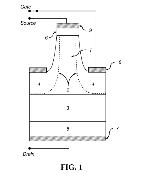
[0050] A schematic cross-section of an exemplary 4H-SiC VJFET structure with
the non-
uniformly doped non-punch-through channel is shown in FIG. 1. Exemplary
channel
doping profiles are shown in FIG. 2. In these figures, the reference numerals
1, 2, and 3
denote the channel region, rectifying junction, and drift region,
respectively. The
reference numerals 4, 5, and 6 in FIG. 1 correspond to the P+ gate regions,
the N+ drain
substrate, and the N+ source layer, respectively. The numerals 101, 102, 103,
and 104 in
FIG. 2 represent exemplary doping profiles in the channel and drift regions.
Latin
12
CA 02722942 2010-10-28
WO 2009/137578 PCT/US2009/042983
numerals I and II in FIG. 2 represent conditionally defined "VTH-control" and
"field-
stop" portions of the channel that have lengths L1 and L2, respectively.
[0051] The doping profiles shown in FIG. 2 are merely exemplary. Moreover, the
doping
distribution along the channel can be optimized to provide the highest voltage
gain during
turn-off while minimizing the channel resistance and the effect of the current
saturation in
the on-state. For example, the doping profile can be defined by a higher
degree
polynomial or by another analytical function.
[0052] As discussed above, the devices described herein have non-punch-through
channels with significantly reduced resistance, which can be achieved by
increasing the
channel doping concentration while maintaining a sufficient distance between
the
rectifying junctions. This can result in more pronounced junction
singularities at the
channel entrances resulting in more significant field enhancement that
ultimately lowers
the maximum allowed 1-D electric field applied to the gate-drift junction.
Moreover,
when trying to increase the channel packing density by reducing the trench
width, the
radii of the gate junction "cylinders" can be reduced resulting in further
field
enhancement.
[0053] In order to suppress the electric field enhancement at the rectifying
junctions, a
device having a relatively thin semiconductor layer located at the drain
entrance of the
channel between the higher doped "field-stop channel" and lower doped drift
region is
also provided. Exemplary doping profiles in a non-uniformly doped NPT channel
having
a gradually and stepwise doped field suppressing layer, or "field-smooth
channel," are
shown in FIGS. 3A and 3B, respectively. The reference numerals 201-204 and 301-
304
in FIGS. 3A and 3B schematically represent exemplary doping profiles in the
channel and
drift regions in the case of gradually (FIG. 3A) and stepwise (FIG. 3B) doped
"field-
13
CA 02722942 2010-10-28
WO 2009/137578 PCT/US2009/042983
smooth channels." Latin numerals I, II, and III in these figures represent
conditionally
defined "VTH-control", "field-stop", and "field-smooth" portions of the
channel that have
lengths L1, L2, and L3, respectively. As in the previous embodiments, the
doping
concentration in the "field-smooth" portion of the channel can be defined by a
higher
degree polynomial or by another analytical function.
[0054] According to some embodiments, a device having a non-uniformly doped
channel
as described above is provided wherein the rectifying junctions confining the
current flow
are electrically coupled or biased independently or wherein at least one of
the rectifying
junctions is electrically coupled to one of the channel entrances.
[0055] A non-uniformly doped channel as described above can be used to control
the
current flow in field-effect semiconductor devices having a vertical channel
structure
including, but not limited to, Junction Field-Effect Transistors (JFETs),
Static Induction
Transistors (SITs), Junction Field Effect Thyristors, and JFET current
limiters.
[0056] For example, the non-uniformly doped channel described above can be
used to
control the current flow in normally-off SiC Vertical Junction Field-Effect
Transistors
(VJFETs).
[0057] The average doping concentration calculated along the current flow path
in the
"VTH-control" portion of the channel may range from 1 x 10¹⁶ CM -3 to 1 x 10¹⁷
cm 3.
[0058] The average distance between the rectifying junctions in the "VTH-
control"
portion of the channel can be selected to provide a desired threshold voltage
and may
range from 0.3 gm to 1.7 gm.
[0059] The length of the "VTH-control" portion of the channel measured along
the
current flow path may vary from 0.25 gm to 1 gm.
14
CA 02722942 2010-10-28
WO 2009/137578 PCT/US2009/042983
[0060] The average doping concentration in the "field-stop" portion of the
channel can be
from 3x1016cm3to3x1017cm3.
[0061] The length of the "field-stop" portion of the channel measured along
the current
flow path may vary from 0.5 gm to 3 gm.
[0062] The length of the optional "field-smooth" portion of the channel
measured along
the current flow path may vary from 0.25 gm to 0.75 gm.
[0063] The average doping concentration of the optional "field-smooth" portion
of the
channel calculated along the current flow path may vary from 1 x 10¹⁶ CM -3 to
1 x 10¹⁷
-3
cm .
[0064] According to some embodiments, the device has a channel with a punch-
through
electric field (i.e., the minimum electric field which, when applied to the
channel, results
in punch-through behavior) which is greater than 2.4 MV/cm. For example, the
device
can exhibit non-punch through behavior at an applied electric field of 2.4
MV/cm or less.
[0065] The device having a non-uniformly doped channel can be a normally-off
junction
field-effect transistors (JFET) made of a wide bandgap semiconductor (e.g., a
semiconductor material having EG > 2 e V) and having a vertical channel
structure
confined with either implanted or regrown p-n junctions, or by rectifying
Schottky
contacts. This non-uniformly doped channel can also be used in the design and
fabrication of other wide bandgap semiconductor devices having a vertical
channel
structure. Examples of such devices include, but are not limited to, Junction
Field-Effect
Transistors (JFETs), Static Induction Transistors (SITs), Junction Field
Effect Thyristors,
and JFET current limiters.
CA 02722942 2010-10-28
WO 2009/137578 PCT/US2009/042983
[0066] Moreover, the device can be any semiconductor device having a vertical
channel
structure where the current flow is confined by the rectifying junctions.
Examples of
such devices include, but are not limited to: junction field-effect
transistors and thyristors
where the current flow occurs through a lateral channel connected in series
with a vertical
channel; Metal Oxide Semiconductor Field Effect Transistors (MOSFETs) where
the
current flow occurs through a MOS channel connected in series with a vertical
channel
confined with the p-n junctions; and Junction Barrier Schottky (JBS) diodes,
where the
current flow occurs through the channel confined with the p-n junctions.
[0067] As set forth above, the semiconductor devices can be made in a wide
band gap
semiconductor material such as SiC. The SiC can be 4H-SiC. Other polytypes of
SiC
(e.g., 6H-SiC, 3C-SiC, or 15R-SiC) or other wide bandgap semiconductor
materials such
as Group III nitride compound semiconductors (e.g., gallium nitride GaN),
however, can
also be used.
[0068] The non-uniformly doped channel structure described herein can provide
non-
punch-through behavior with minimum resistance for a given threshold voltage.
The
non-uniform doping concentration in the channel region can be achieved using
epitaxial
growth. For example, by using epitaxial reactors that allow specifying gas
flow as
analytical functions of time (e.g., see Reference [7]). Alternatively, the non-
uniform
doping concentration in the channel region can be achieved via multi-dose ion
implantation.
[0069] Although modern commercial epitaxial reactors allow specifying gas flow
as
analytical functions of time (e.g., see Reference [7]) to define non-uniform
doping
concentrations, the resulting doping profiles can differ from those expected.
Because the
required doping concentration incorporated into the grown "field-stop" and
"VTH-
16
CA 02722942 2010-10-28
WO 2009/137578 PCT/US2009/042983
control" layers may decrease with time during the epitaxial run, a so-called
memory
effect may result in unintentional doping in addition to the analytically
specified doping
concentration. The "memory effect" can be caused by the dopant species being
absorbed
by internal surfaces of the epitaxial reactor in the early stages of epitaxial
growth. The
effect can be compensated for by adding correction terms to the analytical
formulas that
define the gas flow.
[0070] In the case of using ion-implantation to form non-uniform doping
profiles, such
profiles would experience the "valleys" between the concentration peaks
corresponding to
implantation energies. In order to minimize the influence of such "valleys"
between the
concentration peaks, the implantation schedule (i.e., energies and doses) can
be carefully
designed.
[0071] Zero-degree ion implantation can be used to form the rectifying
junctions. The
use of zero-degree ion implantation can significantly reduce the amount of
implantation
damage propagating to the channel laterally thereby significantly reducing the
effect of
the current saturation (more than an order of magnitude higher saturation
current density
at VGS = 2.5 V). According to some embodiments, the ion implantation can be
conducted
at an angle within +/- 2 degrees of perpendicular to the substrate. According
to some
embodiments, the ion implantation can be conducted at an angle within +/- 1
degree of
perpendicular to the substrate.
[0072] FIG. 4 shows overlaid measured and simulated IN characteristics of a 1
mm2
normally-off 1500 V 4H-SiC VJFET with a channel having uniform doping
concentration
of 5 x 10¹⁶ CM -3 and rectifying junctions formed using zero-degree ion-
implantation.
[0073] FIG. 5A is a graph showing simulated I-V characteristics for a 1 mm2
normally-
off 800 V SiC VJFET with rectifying junctions formed using zero-degree ion-
17
CA 02722942 2010-10-28
WO 2009/137578 PCT/US2009/042983
implantation having uniform channel doping. FIG. 5B is a pie chart showing the
components of the total resistance for a 1 mm2 normally-off 800 V SiC VJFET
with
rectifying junctions formed using zero-degree ion-implantation having uniform
channel
doping.
[0074] FIG. 6A is a graph showing simulated I-V characteristics for a 1 mm2
normally-
off 800 V SiC VJFET with rectifying junctions formed using zero-degree ion-
implantation having non-uniform channel doping. FIG. 6B is a pie chart showing
the
components of the total resistance for a 1 mm2 normally-off 800 V SiC VJFET
with
rectifying junctions formed using zero-degree ion-implantation having non-
uniform
channel doping.
[0075] The drift parameters in both devices were calculated using equation (1)
for the
E/Drrax and Vb equal to 2.3 MV/cm and 800 V, respectively.
[0076] While the foregoing specification teaches the principles of the present
invention,
with examples provided for the purpose of illustration, it will be appreciated
by one
skilled in the art from reading this disclosure that various changes in form
and detail can
be made without departing from the true scope of the invention.
18
CA 02722942 2010-10-28
WO 2009/137578 PCT/US2009/042983
REFERENCES
[1] J.N. Merrett, I. Sankin, V. Bonderenko, C.E. Smith, D. Kajfez, and J.R.B.
Casady,
"RF and DC Characterization of Self-aligned L-band 4H-SiC Static Induction
Transistors," Materials Science Forum Vols. 527-529 (2006) pp. 1223-1226.
[2] J.H. Zhao, K. Tone, X. Li, P. Alexandrov, L. Fursin and M. Weiner, "3.6
mf2=cm2,
1726V 4H-SiC normally-off trenched-and-implanted vertical JFETs and circuit
applications," IEE Proc. -Circuits Devices Syst., Vol. 151, No. 3, June 2004.
[3] P. Sannuti, X. Li, F. Yan, K. Sheng, J.H. Zhao, "Channel electron mobility
in 4H-
SiC lateral junction field effect transistors, " Solid-State Electronics 49
(2005) 1900-1904
[4] W. Shockley, "A Unipolar "Field-Effect" Transistor," Proceedings of the
IRE
Volume 40, Issue 11, Nov. 1952, pp.:1365 - 1376.
[5] I. Sankin, "Edge termination and RESURF technology in power silicon
carbide
devices," Ph.D. Dissertation, Mississippi State University, 2006; AAT 3213969,
p.110.
[6] M. Nagata, T. Masuhara, N. Hashimoto, H. Masuda, "A short-channel, punch-
through-breakdown-free MOS transistor," International Electron Devices
Meeting, 1971
Volume 17, 1971 Page(s): 2-3.
[7] Legacy CACE User's Guide AixRecipe; Recipe Language for AIXTRON systems,
Copyright 1994-2004, AIXTRON AG, Kaskertstrasse 15-17 D-52072 Aashen, Germany.
19