Note: Descriptions are shown in the official language in which they were submitted.
CA 02723058 2012-08-08
`74769-718E(S)
1
DIRECT CONVERSION RECEIVER ARCHITECTURE
This Is a Divisional Of Canadian Patent Application
Serial No. 2,438,333 Filed February 15, 2002
BACKGROUND
Field
[10011 The present invention relates generally to electronic circuits, and
more
specifically to a direct downconversion receiver architecture for use in a
wireless (e.g.,
CDMA) communication system.
Background
[10021 In a CDMA system, data to be transmitted is initially processed to
generate a
radio frequency (RF) modulated signal that is more suitable for transmission
over a wireless
communication channel. The RF modulated signal is then transmitted over the
communication
channel to one or more intended receivers, which may be terminals in the CDMA
system. The
transmitted signal is affected by various transmission phenomena, such as
fading and
multipath. These phenomena result in the RF modulated signal being received at
the terminals
at a wide range of signal power levels, which may be 100 dB or more.
110031 At a given terminal, the transmitted signal is received, conditioned,
and
downconverted to baseband by a receiver front-end unit. Conventionally, the
frequency
downconversion from RF to baseband is performed with a heterodyne receiver
that includes
multiple (e.g., two) frequency downconversion stages. In the first stage, the
received signal is
downconverted from RF to an intermediate frequency (IF) where filtering and
amplification
are typically performed. And in the second stage, the IF signal is then
downconverted from IF
to baseband where additional processing is typically performed to recover the
transmitted
data.
[10041 The heterodyne receiver architecture provides several advantages.
First, the IF
frequency may be selected such that undesired inter-modulation (IM) products,
which result
from non-linearity in the RF and analog circuitry used to condition and
downconvert the
CA 02723058 2012-08-08
74769-718E(S)
2
received signal, may be more easily filtered. Second, multiple filters and
variable gain
amplifier (VGA) stages may be provided at RF and IF to provide the necessary
filtering and
amplification for the received signal. For example, an RF amplifier may be
designed to provide 40
dB of gain range and an IF amplifier may be designed to provide 60 dB of gain
range, which
would then collectively cover the 100 dB of dynamic range for the received
signal.
[1005] For certain applications, such as cellular telephone, it is highly
desirable to
simplify the receiver design to reduce size and cost. Moreover, for mobile
applications such as
cellular telephone, it is highly desirable to reduce power consumption to
extend battery life
between recharges. For these applications, a direct downconversion receiver
(which is also
known as a homodyne receiver or a zero-IF receiver) may provide these desired
benefits
because it uses only one stage to directly downconvert the received signal
from RF to
baseband.
[1006] Several challenges are encountered in the design of a direct
downconversion
receiver. For example, because there is no IF signal in the direct
downconversion receiver, the
(e.g., 60 dB) gain range normally provided by the IF amplifier in the
heterodyne receiver
would need to be provided instead at either RF or baseband in the direct
downconversion
receiver. To avoid placing additional requirements on the RF circuitry and to
reduce cost and
circuit complexity, this IF gain range may be provided at baseband. However,
if the baseband
gain range is provided digitally after analog-to-digital conversion, then the
baseband signal
provided to the analog-to-digital converter (ADC) would have smaller amplitude
since the
gain is provided digitally after the ADC. DC offset in the baseband signal
would then become
a more critical consideration in the direct downconversion receiver because
the baseband
signal amplitude is smaller, and the DC offset may be a much larger percentage
of the signal
amplitude.
[1007] There is therefore a need in the art for a direct downconversion
receiver
architecture capable of providing the required signal gain and DC offset
correction.
SUMMARY
[1008] Aspects of the invention provide a direct downconversion receiver
architecture
having a DC loop to remove DC offset from the signal components prior to and
after the
CA 02723058 2012-08-08
74769-718E(S)
3
analog-to-digital conversion, a digital variable gain amplifier (DVGA) to
provide a range of
gains, an automatic gain control (AGC) loop to provide gain control for the
RF/analog
circuitry and the DVGA, and a serial bus interface (SBI) unit to provide
controls for the
RF/analog circuitry using a compact serial interface.
[1009] In an aspect, a DVGA is provided for use in the direct downconversion
receiver. The DVGA can provide the required range of gains needed to account
for all or a
portion of the total dynamic range of the received signal (i.e., the portion
not accounted for by
the RF/analog circuitry). The design of the DVGA and the placement of the DVGA
within the
direct downconversion receiver architecture may be advantageously implemented
as described
herein.
[1010] In another aspect, the operating mode of the VGA loop is selected based
in part
on the operating mode of the DC loop. Since these two loops operate (directly
or indirectly)
on the same signal components, they interact with one another. Techniques are
provided
herein for a loop to signal an event that may impact the performance of the
other loop, so that
the other loop can appropriately handle the event to minimize performance
degradation. For
example, if the DC loop is operated in an acquisition mode to quickly remove
large DC
offsets, large DC spikes can be produced that may have various deleterious
effects on the
AGC loop, then this event is triggered and the AGC loop may then be operated
in a low gain
mode or frozen altogether to minimize the effects of the DC spikes on the
operation of the
AGC loop.
[1011] In yet another aspect, the duration of time the DC loop is operated in
the
acquisition mode is inversely proportional to the bandwidth of the DC loop in
the acquisition
mode. The DC loop bandwidth is designed to be wider in the acquisition mode to
allow the
DC loop to more quickly respond to and remove DC offset in the signal
components.
However, the wider loop bandwidth also results in more loop noise generated by
the DC loop.
To limit the amount of total noise (which includes the DC spike to be
corrected and the loop
noise) and still allow the DC loop to operate at high bandwidth, the time
duration in which the
DC loop operates in the acquisition mode may be set inversely proportional to
the loop
bandwidth. Since a wider loop bandwidth
CA 02723058 2012-05-09
74769-718E(S)
4
is able to more quickly correct for the DC offset, a shorter amount of time
spent in the
acquisition mode improves performance.
[1012] In yet another aspect of the invention, the controls for some or all of
the
RF/analog circuitry are provided via a serial bus. The use of a standard
serial bus to
control RF/analog functions provides many advantages, such as reduced pin
count,
simplified board layout, reduced cost, and so on. The serial bus may be
designed
with various features to more effectively provide the controls. For example,
multiple
hardware request channels may be supported (e.g., one channel for each circuit
to
be individually controlled), each channel may be associated with a respective
priority,
and messages may be transmitted on each channel using a number of possible
data
transfer modes.
According to another aspect of the present invention, there is provided
a method of processing a desired signal in a wireless communication system,
comprising: amplifying the desired signal with a first gain having a coarse
resolution;
downconverting the amplified signal from radio frequency (RF) to baseband with
a
single frequency downconversion stage configured to receive a digital offset
control
signal and an analog offset control signal, wherein a gain control value of
the
first gain, the digital offset control signal, and the analog offset control
signal are
derived at least in part from a value of a DC offset of the baseband;
digitizing the
downconverted signal to provide samples; correcting for the DC offset in the
downconverted signal with a DC loop; and digitally amplifying the samples with
a
second gain having a fine resolution to provide output data having a desired
signal
amplitude.
According to yet another aspect of the present invention, there is
provided a direct downconversion receiver comprising: an RF front-end unit
operative
to amplify, downconvert to baseband at essentially constant first gain and at
least
partially based on a digital offset control signal and an analog offset
control signal,
CA 02723058 2012-05-09
74769-718E(S)
4a
and digitize a received signal to provide samples of the baseband, wherein a
gain
control value of the first gain, digital offset control signal, and the analog
offset control
signal are derived at least in part from a value of a DC offset of the
baseband; a
digital variable gain amplifier (DVGA) operative to amplify the samples with a
second gain to provide output data having a desired signal amplitude; and an
automatic gain control (AGC) loop operative to provide the second gain for the
DVGA based in part on the output data.
According to yet another aspect of the present invention, there is
provided an apparatus in a wireless communication system, comprising: first
means
for amplifying a received signal and downconverting to baseband the received
signal
at a first gain and at least partially based on a digital offset control
signal and an
analog offset control signal, wherein a gain control value of the first gain,
the digital
offset control signal, and the analog offset control signal are derived at
least in part
from a value of a DC offset of the baseband; means for cancelling a DC offset
in the
baseband; second means for digitally amplifying the DC offset cancelled
signal; and
means for measuring the digitally amplified signal and to control the gains of
the
first and second amplifying means.
According to yet another aspect of the present invention, there is
provided a receiver unit comprising: an analog variable gain amplifier and a
downconverter for amplifying and downconverting a received signal to baseband
with
a first gain and at least partially based on a digital offset control signal
and an analog
offset control signal, wherein a gain control value of the first gain, the
digital offset
control signal, and the analog offset control signal are derived at least in
part from a
value of a DC offset of the baseband; a DC offset canceller coupled to an
output of
the analog variable gain amplifier; a digital variable gain amplifier
configurable
according to a second gain and coupled to an output of the DC offset
canceller; a
gain controller adapted to measure a signal output from the digital variable
gain
amplifier and to control the first gain and the second gain; and a control
interface
operative to provide the first gain for the analog variable gain amplifier.
CA 02723058 2012-05-09
74769-718E(S)
4b
According to yet another aspect of the present invention, there is
provided a receiver unit comprising: an RF front-end unit operative at a first
gain to
amplify, downconvert to baseband at least partially based on a digital offset
control
signal and an analog offset control signal, and digitize a received signal to
provide
samples, wherein a gain control value of the first gain, the digital offset
control signal,
and the analog offset control signal are derived at least in part from a value
of a
DC offset of the baseband; a DC loop operative to cancel DC offset in the
samples; a
digital variable gain amplifier (DVGA) operative to amplify the DC offset
cancelled
samples with a second gain to provide output data having a desired signal
amplitude;
an automatic gain control (AGC) loop operative to provide the second gain for
the
DVGA and the first gain for the RF front-end unit based in part on the output
data;
and a control interface operative to provide the first gain to the RF front-
end unit.
According to yet another aspect of the present invention, there is
provided a method of processing a received signal in a wireless communication
system, comprising: amplifying and downconverting to baseband a received
signal
with a first variable gain and at least partially based on a digital offset
control signal
and an analog offset control signal; cancelling a DC offset in the
downconverted
received signal; digitally amplifying with a second variable gain the DC
offset
cancelled signal; measuring the digitally amplified signal; and determining
the
first and second variable gains in response to the digitally amplified signal
measurements, wherein a gain control value of the first variable gain, the
digital offset
control signal, and the analog offset control signal are derived at least in
part from a
value of a DC offset of the baseband.
According to yet another aspect of the present invention, there is
provided an apparatus comprising: means for amplifying and downconverting to
baseband a received signal with a first variable gain and at least partially
based on a
digital offset control signal and an analog offset control signal; means for
cancelling a
DC offset coupled to the analog amplifying means; digital means for amplifying
with a
CA 02723058 2012-05-09
74769-718E(S)
4c
second variable gain coupled to an output of the DC offset cancelling means;
means
for measuring a signal output from the digital amplification means and to
control the
first and second variable gains; and means operative to provide the first
variable gain
to the means for amplifying and downconverting, wherein a gain control value
of the
first variable gain, the digital offset control signal, and the analog offset
control signal
are derived at least in part from a value of a DC offset of the baseband.
According to yet another aspect of the present invention, there is
provided a method comprising: amplifying with a first gain, downconverting to
baseband at least partially based on a digital offset control signal and an
analog
offset control signal and digitizing a received signal to provide samples;
cancelling a
DC offset in the samples; digitally amplifying the DC offset cancelled samples
with a
second gain to provide output data; determining the first gain and a second
gain,
based in part on the output data, such that the output data have a desired
signal
amplitude; and providing the first gain to the amplifying, downconverting and
digitizing
means, wherein a gain control value of the first gain, the digital offset
control signal,
and the analog offset control signal are derived at least in part from a value
of a
DC offset of the baseband.
According to yet another aspect of the present invention, there is
provided an apparatus comprising: means for amplifying, downconverting to
baseband at least partially based on a digital offset control signal and an
analog
offset control signal and digitizing a received signal to provide samples at
first gain;
means for cancelling a DC offset in the samples; means for digitally
amplifying the
DC offset cancelled samples with a second gain to provide output data having a
desired signal amplitude; means for determining the first gain and a second
gain
based in part on the output data; and means for providing the first gain to
the
amplifying, downconverting and digitizing means, wherein a gain control value
of the
first gain, the digital offset control signal, and the analog offset control
signal are
derived at least in part from a value of a DC offset of the baseband.
CA 02723058 2012-05-09
74769-718E(S)
4d
According to yet another aspect of the present invention, there is
provided a method, comprising: amplifying a desired signal with a first gain
having a
coarse resolution; downconverting the amplified signal from radio frequency
(RF) to
baseband with a single frequency downconversion stage configured to receive a
digital offset control signal and an analog offset control signal, wherein a
gain control
value of the first gain, the digital offset control signal, and the analog
offset control
signal are derived at least in part from a value of a DC offset of the
baseband;
digitizing the downconverted signal to provide samples; correcting for DC
offset in the
downconverted signal with a DC loop; digitally amplifying the samples with a
second gain having a fine resolution to provide output data having a desired
signal
amplitude.
According to yet another aspect of the present invention, there is
provided an apparatus, comprising: means for amplifying a desired signal with
a
first gain having a coarse resolution; means for downconverting the amplified
signal
from radio frequency (RF) to baseband with a single frequency downconversion
stage configured to receive a digital offset control signal and an analog
offset control
signal, wherein a gain control value of the first gain, the digital offset
control signal,
and the analog offset control signal are derived at least in part from a value
of a
DC offset of the baseband; means for digitizing the downconverted signal to
provide
samples; means for correcting for DC offset in the downconverted signal with a
DC loop; means for digitally amplifying the samples with a second gain having
a fine
resolution to provide output data having a desired signal amplitude.
According to yet another aspect of the present invention, there is
provided a method comprising: amplifying, downconverting from radio frequency
(RF)
to baseband at essentially constant first gain and at least partially based on
a digital
offset control signal and an analog offset control signal, and digitizing a
received
signal to provide samples; digitally amplifying the samples with a variable
CA 02723058 2012-05-09
74769-718E(S)
4e
second gain to provide output data having a desired signal amplitude; and
determining a gain control value of the constant first gain, the digital
offset control
signal, and the analog offset control signal derived at least in part from a
value of a
DC offset of the baseband and the variable second gain based in part on the
output
data.
According to yet another aspect of the present invention, there is
provided an apparatus comprising: means for amplifying, downconverting from
radio
frequency (RF) to baseband at essentially constant first gain and at least
partially
based on a digital offset control signal and an analog offset control signal,
and
digitizing a received signal to provide samples; means for digitally
amplifying the
samples with a variable second gain to provide output data having a desired
signal
amplitude; and means for determining a gain control value of the constant
first gain,
the digital offset control signal, and the analog offset control signal
derived at least in
part from a value of a DC offset of the baseband and the variable second gain
based
in part on the output data.
According to yet another aspect of the present invention, there is
provided a method, operable with an RF module, the RF module comprising an
analog variable gain amplifier amplifying a received radio frequency (RF)
signal
according to a first gain value, the amplifier output coupled to a
downconverter, the
method comprising: downconverting a downconverter input from RF to baseband
at least partially based on a digital offset control signal and an analog
offset control
signal to produce a downconverted signal; digitally amplifying the
downconverted
signal in accordance with a second gain value to produce a digitally amplified
output;
and providing the first gain value and the second gain value with an automatic
gain
control loop to produce the digitally amplified output at a desired signal
amplitude,
wherein a gain control value of the first gain value, the digital offset
control signal,
and the analog offset control signal are derived at least in part from a value
of a
DC offset of the baseband.
CA 02723058 2012-05-09
74769-718E(S)
4f
According to yet another aspect of the present invention, there is
provided an apparatus, adapted to operate with an RF module, the RF module
comprising an analog variable gain amplifier amplifying a received radio
frequency
(RF) signal according to a first gain value, the amplifier output coupled to a
downconverter, the apparatus comprising: means for downconverting a
downconverter input from RF to baseband at least partially based on a digital
offset
control signal and an analog offset control signal to produce a downconverted
signal;
means for digitally amplifying the downconverted signal in accordance with a
second gain value to produce a digitally amplified output; and means for
providing the
first gain value and the second gain value with an automatic gain control loop
to
produce the digitally amplified output at a desired signal amplitude, wherein
a gain
control value of the first gain value, the digital offset control signal, and
the analog
offset control signal are derived at least in part from a value of a DC offset
of the
baseband.
According to yet another aspect of the present invention, there is
provided a method, operable with an RF module, the RF module comprising an
analog variable gain amplifier amplifying a received radio frequency (RF)
signal
according to a first gain value, the amplifier output coupled to a
downconverter, the
method comprising: downconverting a downconverter input from RF to baseband
at least partially based on a digital offset control signal and an analog
offset control
signal to produce a downconverted signal; digitally amplifying the
downconverted
signal in accordance with a second gain value to produce a digitally amplified
output;
measuring the digitally amplified output; and generating the first and second
gain
values, wherein a gain control value of the first gain value, the digital
offset control
signal, and the analog offset control signal are derived at least in part from
a value of
a DC offset of the baseband.
CA 02723058 2012-05-09
74769-718E(S)
4g
According to yet another aspect of the present invention, there is
provided an apparatus, adapted to operate with an RF module, the RF module
comprising an analog variable gain amplifier amplifying a received radio
frequency
(RF) signal according to a first gain value, the amplifier output coupled to a
downconverter, the apparatus comprising: means for downconverting a
downconverter input from RF to baseband at least partially based on a digital
offset
control signal and an analog offset control signal to produce a downconverted
signal;
means for digitally amplifying the downconverted signal in accordance with a
second gain value to produce a digitally amplified output; means for measuring
the
digitally amplified output; and means for generating the first and second gain
values,
wherein a gain control value of the first gain value, the digital offset
control signal,
and the analog offset control signal derived at least in part from a value of
a DC offset
of the baseband.
[1013] Various aspects and embodiments of the invention are described in
further detail below. The invention further provides methods, digital signal
processors, receiver units, and other apparatuses and elements that implement
various aspects, embodiments, and features of the invention, as described in
further
detail below.
BRIEF DESCRIPTION OF THE DRAWINGS
[1014] The features, nature, and advantages of the present invention will
become more apparent from the detailed description set forth below when taken
in
conjunction with the drawings in which like reference characters identify
correspondingly throughout and wherein:
[1015] FIG. 1 is a block diagram of an embodiment of a receiver unit capable
of implementing various aspects and embodiments of the invention;
[1016] FIG. 2A is a block diagram of an embodiment of a direct downconverter;
CA 02723058 2012-05-09
74769-718E(S)
4h
[1017] FIG. 2B is a block diagram of an embodiment of a DC offset canceller;
[1018] FIG. 3 is a block diagram of an embodiment of a digital variable gain
amplifier (DVGA);
[1019] FIG. 4A is a block diagram of an AGC loop unit;
[1020] FIG. 4B is a block diagram of an AGC control unit; and
[1021] FIG. 4C is a diagram of an example gain transfer function for the
RF/analog circuits.
CA 02723058 2010-11-24
WO 02/067420 PCT/US02/04727
DETAILED DESCRIPTION
110221 FIG. I is a block diagram of an embodiment of a receiver unit 100
capable of
implementing various aspects and embodiments of the invention. Receiver unit
100
may be implemented within a terminal or a base station of a wireless (e.g.,
CDMA)
communication system. For clarity, various aspects and embodiments of the
invention
are described for a receiver implementation in a terminal. Also for clarity,
specific
design values are provided herein, but other design values may also be used
and are
within the scope of the invention.
(10231 In FIG. 1, one or more RF modulated signals transmitted from one or
more
transmitters (e.g., base stations, GPS satellites, broadcast stations, and so
on) are
received by an antenna 112 and provided to an amplifier (Amp) 114. Amplifier
114
amplifies the received signal with a particular gain to provide an amplified
RF signal.
Amplifier 114 may comprise one or more low noise amplifier (LNA) stages
designed to
provide a particular range of gains and/or attenuation (e.g., 40 dB from
maximum gain
to attenuation). The specific gain of amplifier 114 may be determined by a
gain control
message provided by a serial bus interface (SBI) unit 150 via a serial bus
152. The
amplified RF signal is then filtered by a receive filter 116 to remove noise
and spurious
signals, and the filtered RF signal is provided to a direct downconverter 120.
(10241 Direct downconverter 120 performs direct quadrature downconversion of
the
filtered RF signal from RF to baseband. This may be achieved by multiplying
(or
mixing) the filtered RF signal with a complex local oscillator (LO) signal to
provide a
complex baseband signal. In particular, the filtered RF signal may be mixed
with an
inphase LO signal to provide an inphase (1) baseband component and mixed with
a
quadrature LO signal to provide a quadrature (Q) baseband component. The mixer
used
to perform the direct downconversion may be implemented with multiple stages
that
may be controlled to provide different gains, as described below. In this
case, the
specific gain to be provided by the mixer may also be determined by another
gain
control message provided by SBI unit 150 via serial bus 152, as shown in FIG.
1. The I
and Q baseband components are then provided to one or more analog-to-digital
converters (ADCs) 122.
(10251 ADCs 122 digitize the I and Q baseband components to provide I and Q
samples, respectively. ADCs 122 may be implemented with various ADC designs,
such
as with sigma-delta modulators capable of filtering and then over-sampling the
I and Q
CA 02723058 2010-11-24
WO 021067420 PCT/US02/04727
6
baseband components at multiple (e.g., 16) times the chip rate of the baseband
components (which is 1.2288 Mcps for IS-95). The over-sampling allows the ADCs
to
provide a higher dynamic range and further allows the I and Q samples to be
provided
with fewer number of bits for a given precision. In a specific embodiment,
ADCs 122
provide 2-bit I and Q samples at 16 times the chip rate (i.e., chipxl6). Other
types of
ADCs may also be used and are within the scope of the invention. The I and Q
samples
are provided from ADCs 122 to a digital filter 124.
[10261 Digital filter 124 filters the I and Q samples to provide filtered I
and Q
samples, respectively. Digital filter 124 may perform any number of functions
such as
image rejection filtering, baseband pulse-matched filtering, decimation,
sample rate
conversion, and so on. In a specific embodiment, digital filter 124 provides
18-bit
filtered I and Q samples at chipx8 to a DC offset canceller 130.
110271 DC offset canceller 130 removes DC offset in the filtered I and Q
samples to
provide DC offset corrected I and Q samples, respectively. In a specific
embodiment,
DC offset canceller 130 implements two DC offset correction loops that attempt
to
remove DC offsets at two different locations in the received signal path - one
at
baseband after the frequency downconversion by direct downconverter 120 and
another
after the digital filtering by filter 124. The DC offset correction is
described in further
detail below.
(10281 A digital variable gain amplifier (DVGA) 140 then digitally amplifies
the
DC offset corrected I and Q samples to provide I and Q data for subsequent
processing
by a digital demodulator 144. In a specific embodiment, DVGA 140 provides 4-
bit I
and Q data at chipx8.
[10291 Digital demodulator 144 demodulates the I and Q data to provide
demodulated data, which may then be provided to a subsequent decoder (not
shown in
FIG. 1). Demodulator 144 may be implemented as a rake receiver that can
concurrently
process multiple signal instances in the received signal. For CDMA, each
finger of the
rake receiver may be designed to (1) rotate the I and Q data with a complex
sinusoidal
signal to remove frequency offset in the I and Q data, (2) despread the
rotated I and Q
data with a complex pseudo-random noise (PN) sequence used at the transmitter,
(3)
decover the despread I and Q data with the channelization code (e.g., a Walsh
code)
used at the transmitter, and (4) data demodulate the decovered I and Q data
with a pilot
recovered from the received signal. Digital filter 124, DC offset canceller
130, DVGA
CA 02723058 2010-11-24
WO 02/067420 PCT/US02/04727
7
140, and digital demodulator 144 may be implemented within one or more
integrated
circuits (ICs), e.g., within a single digital signal processor.
[10301 An automatic gain control (AGC) loop unit 142 receives the I and Q data
from DVGA 140 and a DC_loop_mode signal from DC offset canceller 130, and
provides the gains for various variable gain elements within receiver unit
100_ In an
embodiment, the gains for amplifier 114 and direct downconverter 120 are
provided to
SBI unit 150, which then provides the appropriate gain control messages to
these
elements via serial bus 152. The gain for DVGA 140 is provided directly to the
DVGA
after taking into account the delay from the RF signal input to the input of
the DVGA.
AGC loop unit 142 provides the appropriate gains for amplifier 114, direct
downconverter 120, and DVGA 140 such that the desired amplitude for the I and
Q data
is achieved. The AGC loop is described in further detail below.
110311 A controller 160 directs various operations of receiver unit 100. For
example, controller 160 may direct the operation of the DC offset
cancellation, the AGC
loop, the DVGA, the SBI, and so on. A memory 162 provides storage for data and
program codes for controller 160.
[10321 In a typical receiver design, the conditioning of the received signal
may be
performed by one or more stages of amplifier, filter, mixer, and so on. For
example, the
received signal may be amplified by one or more LNA stages. Also, filtering
may be
provided before and/or after the LNA stages, and is also typically performed
after the
frequency downconversion. For simplicity, these various signal conditioning
stages are
lumped together into the blocks shown in FIG. 1. Other RF receiver designs may
also
be used and are within the scope of the invention. Amplifier 114, direct
downconverter
120, and ADCs 122 form an RF front-end unit for the direct downconversion
receiver.
[10331 The resolution of the I and Q samples at various signal processing
blocks in
FIG. I are provided for illustration. Different number of bits of resolution
and different
sample rates may also be used for the I and Q samples, and this is within the
scope of
the invention.
DC Offset Correction
110341 FIG. 2A is a block diagram of a direct downconverter 120a, which is a
specific embodiment of direct downconverter 120 in FIG. 1. Within direct
downconverter 120a, the filtered RF signal from receive filter 116 is provided
to a mixer
CA 02723058 2010-11-24
VVO 021067420 PCTIUS02103727
8
212, which also receives a (complex) LO signal from a local oscillator 218.
The
frequency of the LO signal may be controlled by a frequency control signal
(which may
be provided via serial bus 152 or some other signal lines) and is set to the
center
frequency of the RF modulated signal being recovered. Mixer 212 then performs
quadrature downconversion of the filtered RF signal with the complex LO signal
to
provide inphase and quadrature components, which are then provided to a summer
214.
110351 A converter 220 receives a digital DC offset control, which may be
provided
by DC offset canceller 130 via serial bus 152 and is denoted as SBI DC control
in FIG.
2A. Converter 220 then performs digital-to-analog conversion of the digital
control to
generate DC offset control values of DC I I and DC 1 Q for the mphase and
quadrature
components, respectively. In an embodiment, these values are used to control
the bias
current of mixer 212 such that the DC offset in the signal components may be
adjusted
indirectly.
[10361 Analog circuitry 222 receives an analog DC offset control, which may be
provided by DC offset canceller 130 via a dedicated signal line and denoted as
coarse
DC offset in FIG. 2A. Analog circuitry 222 then performs filtering and
possibly level
shifting and scaling to generate DC offset values of DC2I and DC2Q for the
inphase
and quadrature components, respectively. Summer 214 then subtracts the DC ofi-
set
values of DC2I and DC2Q from the inphase and quadrature components,
respectively.
The output components from summer 214 are then filtered and amplified by a
lowpass
filter/amplifier 216 to provide the I and Q baseband components.
[1037j FIG. 2B is a block diagram of a DC offset canceller 130a, which is a
specific
embodiment of DC offset canceller 130 in FIG. 1. DC offset canceller 130a
includes
summers 232a and 232b, DC loop control units 234a and 234b, an SBI DC offset
controller 240, and a DC loop controller 242. In an embodiment, the DC offset
correction is performed separately for the I and Q samples. Thus, summers 232a
and
232b and DC loop control units 234a and 234b each includes two elements, one
to
process the I samples and another to process the Q samples.
[10381 The filtered I and Q samples from digital filter 124 are provided to
summer
232a, which removes fixed DC offset values of DC31 and DC3Q from the I and Q
samples, respectively. Summer 232a may be used to remove DC offset that is
static
(e.g., caused by circuit mismatch and so on). The I and Q outputs from summer
232a
are then provided to summer 232b, which further removes DC offset values of
DC41
CA 02723058 2012-05-09
74769-718E(S)
9
and DC4Q (which-are provided by DC loop control unit 234b) from these I and Q
outputs to provide the DC offset corrected Land Q samples.
[1039] DC loop control unit 234a receives the I and Q outputs from summer
232a,
determines the DC offsets in these outputs, and provides the coarse DC control
to
analog circuitry 222 within direct downconverter 120a. DC loop control unit
234b
similarly receives the I and Q outputs from-summer 232b, determines the DC
offsets in.
these outputs, and provides the DC offset values of DC4I and DC4Q to summer
234b.
Each DC loop control unit 234 is implemented with a gain element 236 coupled
to an
accumulator 238. Gain element 236 multiplies the input I or Q sample with a
particular
gain (DC gain 1 for unit 234a and DC gain 2 for unit 234b) selected- for that
loop.
Accumulator 238 then accumulates the scaled I or Q sample to provide the DC
offset
control for that loop.
[1040] Summer 214 within direct downconverter 120a and DC loop control unit
234a implement a coarse-grain DC loop that- removes DC offset in the baseband
components after the direct downconversion by mixer 212. Summer 232b and DC
loop
control unit 234b implement a fine-grain DC loop that removes.DC offset that
still
remains after the coarse-grain DC loop. As their names imply, the fine-grain
DC loop
has higher resolution than the coarse-grain DC loop.
[1041] SBI DC offset controller 240 periodically determines the SBI DC offset
control based on various factors such as temperature, the gains of amplifier
114 and
mixer 212,. time, drift, and so on. The SBI DC offset control is then provided
via serial
bus 152 to converter 220, which then generates the corresponding DC offset
control
values ofDCII and DC1Q for mixer 212.
[1042] An implementation of the DC offset correction for a direct
downconversion
receiver, such as the one shown in FIG. 1, is described in. further detail in
U.S. Patent
No. 6,985,711, entitled "Direct- Current Offset Cancellation for Mobile
Station Modems
Using Direct Downconversion," issued January 10, 2006.
[10431' The four sets of DC offset values (DC1I and DC1Q, DC2I and DC2Q, DC3I
and DC3Q, and DC4I and DC4Q) represent four different mechanisms that may be
used
individually or in combination to provide the required DC offset correction
for the direct
downconversion receiver. The coarse-grain DC loop (which provides the values
of
DC21 and DC2Q) and the fine-grain DC loop (which provides the values of DC4I
and
CA 02723058 2010-11-24
WO 021067420 PCT/US02/04727
DC4Q) may be operated to dynamically remove DC offset in the I and Q signal
components. Summer 232a (which subtracts the values of DC3I and DC3Q) may be
operated to remove static DC offset. And S13I DC offset controller 240 (which
provides
the values of DCII and DCIQ) may be used to remove dynamic and/or static DC
offset
in the signal components.
110441 In an embodiment, the coarse-grain and fine-grain DC loops each
supports
two operating modes - an acquisition mode and a tracking mode. The acquisition
mode
is used to more quickly remove large DC offset that may have been introduced
in the
signal components as a result of (1) a step change in the gains of the
RF/analog circuitry
such as amplifier 114 and/or mixer 212, or (2) the overall DC loop performing
a
periodic DC update, which may result in new values of DCI and/or DC3 being
provided
to mixer 212 and/or summer 232a, or (3) or any other reasons, respectively.
The
tracking mode is used to perform the DC offset correction in a normal manner,
and its
response is slower than that of the acquisition mode. Different or additional
operating
modes may also be supported, and this is within the scope of the invention.
The
acquisition and tracking modes may correspond to two different DC loop gain
values
for DC gain 1 and to two different DC loop gain values for DC gain 2.
[10451 For simplicity, the coarse-grain and fine-grain DC loops are
collectively
referred to as simply the "DC loop". The DC_loop_mode control signal indicates
the
DC loop's current operating mode. For example, the DC_loop_mode control signal
may be set to logic high to indicate that the DC loop is operating in the
acquisition
mode and to logic low to indicate that it is operating in the tracking mode.
Digital VGA
[1046j A n aspect of the invention provides a DVGA for use in a direct
downconversion receiver. The DVGA can provide the required range of gains
needed
to account for all or a portion of the total dynamic range for the received
signal (i.e., the
portion not accounted for by the RF/analog circuitry). The DVGA's gain range
may
thus be used to provide the gain previously provided at intermediate frequency
(IF) in a
heterodyne receiver. The design of the DVGA and the placement of the DVGA
within
the direct downconversion receiver architecture may be advantageously
implemented as
described below.
CA 02723058 2010-11-24
WO 02/067420 PCT/US02/04727
11
110471 FIG. 3 is a block diagram of a DVGA 140a capable of providing digital
baseband gain for I and Q samples. DVGA 140a is a specific embodiment of DVGA
140 in FIG. 1.
110481 Within DVGA 140a, the DC offset corrected I and Q samples from the
preceding DC offset canceller 130 are provided to a multiplexer (MUX) 312 and
a
truncation unit 320. To minimize hardware, only one digital multiplier 316 is
used to
perform the gain multiplication for both I and Q samples in a time division
multiplexed
(TDM) manner. Thus, multiplexer 312 alternately provides an I sample and then
a Q
sample (as determined by an IQ_sel control signal) to multiplier 316 via an
AND gate
314. The IQ_sel control signal is simply a square wave at the I and Q sample
rate (e.g.,
chipx8) and having the appropriate phase (e.g., logic low for the I samples).
AND gate
314 performs an AND operation of the I or Q sample with a DVGA_enb control
signal,
which is set to logic high if the DVGA is enabled and set to logic low if the
DVGA is
bypassed. The DVGA may be bypassed, for example, if the DVGA's gain range is
not
needed or if the gain range is provided with analog circuitry (e.g., a
variable gain
amplifier). AND gate 314 thus passes the sample to multiplier 316 if the DVGA
is
enabled and provides a zero otherwise. The zero reduces power consumption by
the
subsequent circuitry by eliminating transitions that consume power in CMOS
circuits.
[10491 Multiplier 316 multiplies the I or Q sample from AND gate 314 with a
gain
from a register 344 and provides the scaled (or amplified) sample to a
truncation unit
318. In a specific embodiment, multiplier 316 is operated at twice the sample
rate,
which is chipxl6 for IJQ sample rate of chipx8. In a specific embodiment, for
CDMA
and GPS, the input I and Q samples have 18 bits of resolution with 10 bits of
resolution
to the right of the binary point (i.e., 18Q10), the gain has 19 bits of
resolution with 12
bits of resolution to the right of the binary point (i.e., 19Q12), and the
scaled samples
have 37 bits of resolution with 22 bits of resolution to the right of the
binary point (i.e.,
37Q22). In a specific embodiment, for digital FM or DFM, the input I and Q
samples
have a resolution of 18Q6, the gain has a resolution of 19Q12, and the scaled
samples
have a resolution of 37Q18. Truncation unit 318 truncates the (e.g., 18) least
significant
bits (LSBs) of each scaled sample and provides the truncated sample (which has
a
resolution of 18Q4 for CDMA/GPS and 18Q0 for DFM) to one input of a
multiplexer
322.
CA 02723058 2010-11-24
WO 02/067420 PCT/IJS02/04727
12
110501 For certain operating modes of the receiver, the digital scaling by
DVGA
140a is not needed and the input I and Q samples may be passed to the DVGA's
output
without any scaling (after the appropriate processing to obtain the desired
output data
format). Truncation unit 320 truncates the (e.g., 6) LSBs of each input sample
and
provides the truncated sample to the other input of multiplexer 322.
Truncation unit
320 ensures that the output I and Q data have the same resolution regardless
of whether
the DVGA is enabled or bypassed.
(1051) Multiplexer 322 then provides the truncated sample from either
truncation
unit 318 or 320 depending on whether the DVGA is enabled or bypassed,
respectively,
which is determined by the DVGA_enb control signal. The selected sample is
then
provided to a saturation unit 324, which saturates the sample to the desired
output data
format, e.g., a resolution of 8Q4 for CDMA/GPS and 8Q0 for DFM. The saturated
sample is then provided to a delay element 326 and to one input of a register
328. Delay
element 326 provides one-half sample period of delay to align the I and Q data
(which
have been skewed by one-half sample period to implement the time division
multiplexing for multiplier 316) and provides the delayed I sample to the
other input of
register 328. Register 328 then provides the I and Q data, with the timing
aligned to the
IQ_scl control signal. For CDMA/GPS, the four most significant bits (MSBs) of
the I
and Q data (i.e., with a resolution of 4Q0) is sent to the next processing
block. And for
DFM, the I and Q data (i.e., with a resolution of 8Q0) is sent directly to an
FM
processing block.
110521 Receiver unit 100 may be used for various applications such as to
receive
data from a CDMA system, a GPS system, a digital FM (DFM) system, and so on.
Each such application may be associated with a respective received signal
having some
particular characteristics and requiring some particular gain. As shown in
FIG. 3, the
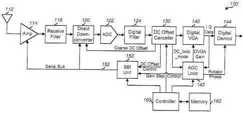
three different gains to be used for CDMA, GPS, and DFM are provided to a
multiplexer 332. One of the gains is then selected based on a Mode _set
control signal.
The selected gain is then provided to a gain scaling and offset unit 334,
which also
receives a gain offset.
[10531 Gain scaling and offset unit 334 scales the selected (CDMA, GPS, or
DFM)
gain with an appropriate scaling factor such that the desired gain resolution
is achieved.
For example, the CDMA gain may be provided with a fixed number of bits (e.g.,
10
bits) that cover one of several possible gain ranges (e.g., 102.4 dB and 85.3
dB gain
CA 02723058 2010-11-24
WO 02/067420 PCT/US02/04727
13
ranges for the 10-bit CDMA gain), depending on the particular mode used for
CDMA.
The scaling factor is then selected such that the scaled CDMA gain has the
same gain
resolution (e.g., 0.13 dB) regardless of the particular mode used for CDMA.
Gain
scaling and offset unit 334 further subtracts the gain offset from the scaled
gain. The
gain offset is determined based on a setpoint selected for ADCs 122, which in
turn
determines the average power of the I and Q baseband components provided to
the
ADCs. The gain offset may be a programmable value having the same resolution
as the
scaled gain, and may be provided by controller 160.
[1054] A multiplexer 336 receives the scaled and offsetted gain from unit 334
and
an override gain and provides one of the gains (based on a Gain override
control signal)
to a saturation unit 338. The override gain may be used instead of the gain
from the
VGA loop, if it is desired to bypass the VGA loop. Saturation unit 338 then
saturates
the received gain (e.g., to 9 bits) to limit the range of the saturated gain
(e.g., to 68.13
dB of total gain range for 9 bits, with 0.133 dB of resolution for each bit).
An AND
gate 340 then performs an AND operation on the saturated gain with the DVGA
enb
control signal, and passes the saturated gain to a dB-to-linear look-up table
(LUT) 342 if
the DVGA is enabled or a zero otherwise (again, to reduce power consumption by
the
subsequent circuitry).
[1055] In an embodiment, the AGC loop provides the gain value (e.g_, the CDMA
gain) in logarithm (dB) format. The dB gain value may be used to mimic the
characteristics of RF/analog variable gain circuits, which typically have log.
(or log-like)
transfer functions for gain versus control value. Secondly, the receive gain
is used as an
estimate for the required transmit power in a CDMA phone call and to report
the receive
power to the base station when requested. These estimations are traditionally
done in
dB given the wide dynamic range of the received signal. However, since a
linear digital
multiplier 316 is used to provide the baseband gain multiplication, the dB
gain value is
translated to a linear gain value. Look-up table 342 performs the dB-to-linear
translation based on a formula, which may be expressed as:
Y(linear) = IOx12Q , Eq (1)
where Y is the linear gain value from the look-up table and X is an
attenuation value,
which may be defined as:
CA 02723058 2010-11-24
WO 02/067420 PCT/tJSO2/04727
14
X = -(Z(dB) + offset) , Eq (2)
where Z is the dB gain value provided to the look-up table and the offset in
equation (2)
may be used to compensate for the truncation performed in unit 334 (e.g.,
offset = 0.067
dB for a 4-bit truncation). Other techniques for converting dB gain value to
linear gain
value may also be used, and this is within the scope of the invention. The
linear gain
value from LUT 342 is then clocked by register 344 to align the timing of the
gain value
with that of the I or Q sample provided to multiplier 316.
110561 The AGC loop may also be designed to operate based on linear (instead
of
dB) gain values, and this is within the scope of the invention.
[10571 Referring back to FIG. 1, DVGA 140 is placed after DC offset canceller
130
and outside of the DC loop in direct downconversion receiver 100. This DVGA
placement provides several advantages and further avoids several
disadvantages. First,
if the DVGA is placed within the DC loop, then any DC offset will be amplified
by the
gain of the DVGA, which would then exacerbate the degradation caused by the DC
offset. Second, the loop gain of the DC loop would also include the gain of
the DVGA,
which varies depending on the received signal strength. Since this DC loop
gain
directly affects (or determines) the bandwidth of the DC loop, the DC loop
bandwidth
would then vary along with the gain of the DVGA, which is an undesirable
effect. The
DC loop bandwidth may be maintained approximately constant by dynamically
changing the DC loop gain (i.e., DC gains 1 and 2 within DC loop units 234a
and 234b)
in an inverse manner to any change in the DVGA gain, so that the overall DC
loop gain
is maintained constant. However, this would further complicate the design of
the DC
offset correction mechanisms. Moreover, the residual DC offset is variable
when
referenced to the actual signal power.
[10581 By advantageously placing DVGA 140 after DC offset canceller 130 and
outside of the DC loop, the DC offset correction by the DC loop may be
decoupled from
the signal gain scaling by the DVGA. Moreover, implementation of the DVGA in
the
digital domain after ADCs 122 further simplify the design of the RF/analog
circuitry,
which may lead to reduced cost for the direct downconversion receiver. Since
the
digital gain is provided after ADCs 122, the amplitude of the signal
components
provided to the ADCs could potentially be smaller, which would then require
greater
dynamic range for the analog-to-digital conversion process so that the ADC
noise does
CA 02723058 2010-11-24
WO 021067420 PCTIUS02/0-4727
not significantly degrade the SNR of the quantized I and Q samples. ADCs with
high
dynamic range may be provided by over-sampling sigma-delta modulators, as is
known
in the art.
Automatic Gain Control
[1059] FIG. 4A is a block diagram of an AGC loop unit 142a, which is a
specific
embodiment of AGC loop unit 142 in FIG. 1. Within AGC loop unit 142a, the I
and Q
data is provided to a received signal strength indicator (RSSI) 412, which
estimates the
signal strength of the received signal. The received signal strength, RSS, may
be
estimated as follows:
NE
RSS = y {I2 (i) + QZ (i )} Eq (3)
where 1(i) and Q(i) represent the I and Q data for the i-th sample period, and
NE is the
number of samples to be accumulated to derive the received signal strength
estimate.
Other techniques may also be used to estimate the received signal strength
(e.g.,
RSS = Il IF(i) I + I QF(i) I ). The received signal strength estimate is then
provided to
an AGC control unit 414.
[1060] FIG. 4B is a block diagram of an AGC control unit 414a, which is a
specific
embodiment of AGC control unit 414 in FIG. 4A. AGC control unit 414a receives
the
received signal strength estimate, RSS, from RSSI 412, the DC_loop_mode
control
signal from DC offset canceller 130, a Nonbypass/hold control signal from gain
step
control unit 418, a delayed gain step decision from a programmable delay unit
420, and
a Freeze-crib control signal (e.g., from controller 160), all of which are
described in
further detail below. Based on the received control signals and RSS, AGC
control unit
414a provides an output gain value that is indicative of the total gain
(G,,,,,,) to be
applied to the received signal.
[1061] In an embodiment, the AGC loop supports three loop modes - a normal
mode, a low gain mode, and a freeze mode. The normal mode is used to provide a
nominal AGC loop bandwidth, the low gain mode is used to provide a smaller AGC
loop bandwidth, and the freeze mode is used to freeze the AGC loop. The low
gain and
normal modes are associated with AGC loop gain values of AGC gain I and AGC
gain
CA 02723058 2010-11-24
WO 02/067420 PCT/US02/04727
16
2, respectively. The freeze mode is achieved by zeroing out the value provided
for
accumulation by the AGC loop accumulator. In an embodiment, an additional AGC
loop gain value of AGC gain 3 is used for jammer detection. AGC gain 3 is
typically
smaller than AGC gain 2 for the normal mode but larger than AGC gain 1 for the
low
gain mode, and is used to detect for the presence of jammer in the signal
components, as
described below. Different or additional modes may also be supported by the
AGC
loop, and this is within the scope of the invention.
[1062] As noted above, the DC loop affects the performance of the AGC loop.
Thus, in an aspect, the specific AGC loop mode to use is dependent on (i.e.,
selected
based on) the specific DC loop mode currently in use. In particular, the
normal mode is
used for the AGC loop when the DC loop is operated in the tracking mode, and
the low
gain or freeze mode is used for the AGC loop when the DC loop is operated in
the
acquisition mode.
[1063] As shown in FIG. 4B, the AGC gain 2 for the normal mode and the AGC
gain 3 for jammer detection are provided to a multiplexer 446, which also
receives the
Nonbypass/hold control signal. The Nonbypass/hold control signal may be used
to
provide time hysteresis between gain steps (i.e., the AGC loop is maintained
at a given
gain step for a particular amount of time (Time 1 or Time 2) before it is
allowed to
switch to another (higher or lower) gain step.
[1064] Multiplexer 446 then provides the AGC gain 2 when the normal mode is
selected, which is indicated by the Nonbypass/hold control being set to logic
low..
Alternatively, multiplexer 446 provides the AGC gain 3 when jammer detection
is to be
performed, which is indicated by the Nonbypass/hold control being set to logic
high. A
multiplexer 448 receives the AGC gain I for the low gain mode and the output
from
multiplexer 448 at its two inputs and further receives the DC_loop_mode
control signal.
Multiplexer 448 then provides the AGC gain 1 to a multiplier 442 when the low
gain
mode is selected for the AGC loop when the DC loop is in the acquisition mode,
which
is indicated by the DC_loop_mode control being set to logic high.
Alternatively,
multiplexer 448 provides the AGC gain 2 or AGC gain 3 to multiplier 442 during
the
tracking mode, which is indicated by the DC_loop_mode control being set to
logic low.
[1065] An AND gate 440 receives the received signal strength estimate, RSS,
and
the Freeze_enb control. AND gate 440 then provides the RSS to multiplier 442
when
(1) the DC loop is operated in the tracking mode or (2) the low gain mode is
used for
CA 02723058 2010-11-24
WO 02/067420 PCT/US02/0-1727
17
the AGC loop when the DC is operated in the acquisition mode. Alternatively,
AND
gate 440 provides a zero to multiplier 442 when the DC loop is operated in the
acquisition mode and the AGC loop is frozen. The zero from AND gate 440
results in
an accumulation of zero by AGC loop accumulator 444 when the AGC loop is
frozen.
[10661 Multiplier 442 multiplies the received signal strength estimate, RSS,
with the
selected AGC gain from multiplexer 448 and provides the result to AGC loop
accumulator 444. Accumulator 444 then accumulates the result with the stored
value
and provides an output gain value that is indicative of the total gain,
Gtotal, to be applied
to the received signal to achieve the desired signal level, which is
determined by the
gain offset provided to gain scaling and offset unit 334 in FIG. 3. This total
gain may
be decomposed into two parts - (1) a coarse gain, Gcoarse, for the RF/analog
circuitry
(e.g., amplifier 114 and mixer 212) and (2) a fine gain, Gfne, for DVGA 140.
The total
gain for the received signal may thus be expressed as:
Gi.rat = G .arse + G f1e , Eq (4)
where Gtotar, Gcoarse, and GfRe are all given in dB.
[10671 As shown in FIG. 4B, accumulator 444 also receives the delayed gain
step
decision, which is indicative of the specific discrete gain to be used for the
RF/analog
circuits, as described below. Each discrete gain for the RF/analog circuits
may be
associated with a respective set of maximum and minimum values for the
accumulation,
which ensures stability in the AGC loop. For the specific discrete gain to be
used, as
indicated by the delayed gain step decision, the proper set of maximum and
minimum
values is used for the accumulation by accumulator 444.
[10681 Referring back to FIG. 4A, the coarse gain control for the RF/analog
circuits
is achieved by (1) mapping the total gain, Gtotar, into a gain step decision
by a gain step
control unit 418, (2) encoding the gain step decision into the appropriate
gain step
controls by a range encoder 424, (3) formatting the gain step controls into
the proper
messages by SBI unit 150, (4) sending the messages to the RF/analog circuits
(e.g.,
amplifier 114 and/or mixer 212) via serial bus 152, and (5) adjusting the
gains of the
RF/analog circuits based on the messages. The fine gain control is achieved by
(1)
determining the fine gain, Gfõej for the DVGA by subtracting the coarse gain,
Gcoarse,
from the total gain, Gtotar, and (2) adjusting the gain of the DVGA based on
the fine
CA 02723058 2010-11-24
WO 02/067420 PCT/US02/04727
18
gain. The derivation of the coarse and fine gains based on the total gain is
described
below.
[10691 Receiver unit 100 may be designed with amplifier 114 having multiple
(e.g.,
four) stages and mixer 212 having multiple (e.g., two) stages. Each stage may
be
associated with a specific discrete gain. Depending on which stages are turned
ON/OFF, different discrete gains may be achieved. The coarse gain then
controls the
gains of the RF/analog circuits in coarse discrete steps. The specific
discrete gain to be
used for the RF/analog circuits is dependent on the received signal level, the
specific
designs of these circuits, and so on.
[10701 FIG. 4C is a diagram of an example gain transfer function for the
RF/analog
circuits (e.g., amplifier 114 and mixer 212). The horizontal axis represents
the total
gain, which is inversely related to the received signal strength (i.e., higher
gain
corresponds to smaller received signal strength). The vertical axis represents
the gain
step decision provided by gain step control unit 418 based on the total gain.
In this
specific example design, the gain step decision takes on one of five possible
values,
which are defined in Table 1.
Table I
Gain RF/Analog
Step Circuit State Definition
Decision
000 first lowest gain - all LNA stages are OFF; mixer is in low gain
001 second second lowest gain - all LNA stages are OFF; mixer is in
high gain
010 third third highest gain - one LNA stage is ON; mixer is in high
ain
O11 fourth second highest gain - two LNA stages are ON; mixer is in
high gain
100 fifth highest gain - all three LNA stages are ON, mixer is in
high gain
[10711 As shown in FIG. 4C, hysteresis is provided in the transition between
adjacent states. For example, while in the second state ("001"), the first LNA
is not
turned ON (to transition to the third state "010") until the total gain
exceeds the L2 Rise
threshold, and this LNA is not turned OFF (to transition from the second back
to the
first state) until the total gain falls below the L2 Fall threshold. The
hysteresis (L2 Rise
CA 02723058 2010-11-24
VVO 02/067420 PCTIUIS02I04727
19
- L2 Fall) prevents the LNA from being continually turned OFF and ON if the
total gain
is between or near the L2 Rise and L2 Fall thresholds.
[1072] Gain step control unit 418 determines the gain step decision based on
the
total gain, a transfer function such as the one shown in FIG. 4C (which is
defined by the
threshold values), and timing, jammer, and possibly other information. The
gain step
decision is indicative of the specific stages to be turned ON/OFF for
amplifier 114 and
mixer 212, as determined by the transfer function. Referring back to FIG. 4A,
gain step
control unit 418 then provides the gain step decision to programmable delay
element
420 and range encoder 424.
[10731 In an embodiment and as shown in FIG. 1, the control to turn ON or OFF
each stage of amplifier 114 and mixer 212 is provided to these circuits via
serial bus
152. Range encoder 424 receives the gain step decision and provides the
corresponding
gain step control for each specific circuit to be controlled (e.g., one gain
step control for
amplifier 114 and another gain step control for mixer 212). The mapping
between the
gain step decision and gain step controls may be based on a look-up table
and/or logic.
Each gain step control comprises one or more bits and turns ON/OFF the
designated
stages within the circuit to be controlled by that gain step control. For
example,
amplifier 114 may be designed with four stages, and its (2-bit) gain step
control may be
associated with four possible values ("00", 01", "10", and "11") for the four
possible
discrete gains for the amplifier. Mixer 212 may be designed with two stages,
and its (1-
bit) gain step control may be associated with two possible values ("0" and
"1") for the
two possible discrete gains for the mixer. The gain step controls for
amplifier 114 and
mixer 212 are formatted into the proper messages by SBI unit 150, and these
messages
are then sent to the circuits via serial bus 152. Range encoder 424 also
provides to DC
offset canceller 130 a gain step change signal that indicates whether or not
the gain of
the RF/analog circuitry has changed to a new value or step.
[1074) As noted above, the total gain, Grorat, for the received signal may be
decomposed into the coarse gain, Gcoarse, and the fine gain, Gfne. Moreover,
as shown in
FIG. 4A, the fine gain is generated by subtracting the coarse gain from the
total gain by
a summer 416. Since the coarse gain (in the form of the gain step controls) is
provided
to amplifier 114 and mixer 212 via SBI unit 150 and the serial bus, a delay is
introduced
between the time the coarse gain is determined by gain step control unit 418
and the
time the coarse gain is actually applied by the RF/analog circuits. Moreover,
processing
CA 02723058 2010-11-24
WO 021067420 PCI'/US02104727
delay is encountered by the received signal from the RF circuitry to the DVGA
(e.g.,
especially digital filter 124). Thus, to ensure that the coarse gain is
applied by the RF
circuits and removed from the DVGA at the same time (i.e., so that the coarse
gain is
applied only once to any given data sample), a programmable delay is used to
delay the
coarse gain (as indicated by the gain step decision) before it is applied to
DVGA 140.
110751 Programmable delay element 420 provides a particular amount of delay
for
the gain step decision. This delay compensates for the delay introduced by SBI
unit 150
and the delay of the received signal processing path from the RF circuitry to
the DVGA.
This delay may be programmed by writing a delay value to a register. Delay
element
420 then provides the delayed gain step decision.
[10761 A coarse gain conversion unit 422 receives the delayed gain step
decision,
which is indicative of a specific discrete gain for the RF/analog circuits,
and provides
the corresponding coarse gain, Gcoarscõ having the proper range and resolution
(e.g., the
same range and resolution as for the total gain from AGC control unit 414)_
The coarse
gain is thus equivalent to the gain step decision but is provided in a
different format
(i.e., the coarse gain is a high-resolution value whereas the gain step
decision is a digital
(ON/OFF) control). The gain step decision to coarse gain translation may be
achieved
with a look-up table and/or logic. The coarse gain is then subtracted from the
total gain
by summer 416 to provide the fine gain for the DVGA.
[10771 Whenever the gain of the RF/analog circuitry is changed by a coarse
amount
by switching stages ON and OFF, the phase of the signal components typically
rotates
by some particular step amount. The amount of phase rotation is dependent on
which
stages having been switched ON and OFF (as determined by the gain step
decision) but
is typically a fixed value for that particular setting or configuration. This
phase rotation
may result in degradation in the data demodulation process, until a frequency
control
loop is able to correct for the phase rotation.
[10781 In an embodiment, the gain step decision is mapped to a corresponding
rotator phase, which is indicative of the amount of phase rotation in the
received signal
components due to the gain indicated by the gain step decision. The rotator
phase is
then provided to a rotator within digital demodulator 144 and used to adjust
the phase of
the I and Q data to account for the phase rotation introduced by the enabled
gain stages
in the RF/analog circuits. The mapping between gain step decision and rotator
phase
may be achieved with a look-up table and/or logic. Moreover, fine resolution
may be
CA 02723058 2010-11-24
WO 02/067-420 PCT/US02/04727
21
achieved for the rotator phase (e.g., 5.6 resolution may be achieved with 6
bits for the
rotator phase)
DC and AGC Loops Operation
[1079] As shown in FIG. 1, the DC loop operates on the filtered I and Q
samples
from digital filter 124 to remove DC offset, and the AGC loop (via DVGA 140)
then
operates on the DC offset corrected I and Q samples to provide the I and Q
data that is
then provided to digital demodulator 144. The AGC loop also controls the gain
of the
RF/analog circuitry, which in turn affects the amplitude of the I and Q
samples operated
on by the DC loop. The DC loop may thus be viewed as being embedded within the
AGC loop. The operation of the DC loop affects the operation of the AGC loop.
[1080] In a direct downconversion receiver, DC offset (both static and time-
varying)
has more impact on the signal components because of the smaller signal
amplitude.
Large DC offsets (or DC spikes) may be introduced in the signal components by
various
means. First, when the gain of the RF/analog circuitry (e.g., amplifier 114
and mixer
212) is changed in discrete steps by switching ON/OFF stages, large DC offsets
may be
introduced in the signal components due to mismatch in the different stages
being
switched ON/OFF. Second, large DC offsets may also be introduced when the DC
loop
performs DC offset updates whereby different DC offset values of DC3I and DC3Q
are
provided to summer 232a and/or different DC offset values of DC1Q and DC1Q are
provided to mixer 212 via the serial bus.
[1081] Large DC offsets may be removed using various mechanisms of the DC loop
(e.g., the coarse-grain and fine-grain loop DC loops). Moreover, large DC
offsets may
be more quickly removed by operating the DC loop in the acquisition mode.
However,
until they are removed, the large DC offsets have deleterious effects on the
signal
components and may degrade performance.
(1082] First, any unremoved DC offset in the signal components appears as
noise
(whose power is equal to the DC offset) after the despreading operation by
digital
demodulator 144. This noise can degrade performance.
[1083] Second, a large DC offset disrupts the performance of the AGC loop in
several ways. The DC offset adds to the signal components and results in
combined
(DC offset and signal) components having a larger amplitude. This then causes
the
AGC loop to reduce the total gain such that the power of the combined
components is
CA 02723058 2010-11-24
WO 02/067420 PCT/US02/0-4727
22
maintained at the AGC setpoint (e.g., I2 + Q2 = AGC setpoint). The reduced
gain then
causes compression of the desired signal components, with the amount of
compression
being proportional to the magnitude of the DC offset. The smaller amplitude
for the
desired signal components results in a degraded signal-to-quantization-noise
ratio
(SNRQ), which also degrades performance. Moreover, if the DC loop is not able
to
completely remove the large DC offset before the it enters the tracking mode,
then the
residual DC offset would be removed more slowly in the tracking mode. The AGC
loop
would then follow this slow transient response of the DC loop, which then
results in a
prolonged degradation period until the DC and AGC loops both achieve steady
state.
110841 Third, a large DC offset affects the ability to accurately detect
jammers,
which are interfering signals in the desired signal band. A jammer may be
generated by
non-linearity in the circuits in the received signal path. Since non-linearity
in amplifier
114 and mixer 212 are more pronounced when these circuits are operated at high
gains
(i.e., more stages being turned ON), the receiver may detect for jammers right
after any
of these circuits is switched to high gain. Jammer detection may be performed
by
measuring the power of the signal components with RSSI 412 right after the
switch to a
high gain, comparing the measured power against a threshold after a particular
measurement time period, and declaring the presence of a jammer in the signal
components if the measured power exceeds the threshold. If a jammer is
detected, then
the gain of one or more circuits may be reduced to either remove or mitigate
the
jammer. However, in the presence of DC offset introduced by the switch to the
high
gain, it may not be possible to discern whether the increase in the measured
power is
due, to jammer or to the total noise, which includes any unremoved DC offset
and the
increased DC loop noise generated by operating the DC loop in the acquisition
mode to
quickly remove the DC offset. Thus, the presence of DC offset may impact the
ability
to accurately detect for jammers, which may degrade performance if the
RF/analog
circuits are operated at the wrong gains due to erroneous detection of
jammers.
[10851 A large DC offset may cause long bursts of errors due to various
deleterious
effects described above. The degradation due to DC offset is more problematic
at
higher data rates since the time needed to remove DC spikes may be fixed
(e.g., by the
specific design of the DC loop), which then results in more errors at higher
data rates.
[10861 In accordance with another aspect of the invention, the duration of
time the
DC loop is operated in the acquisition mode is inversely proportional to the
bandwidth
CA 02723058 2010-11-24
WO 02/067120 PC17US02/04727
23
of the DC loop in the acquisition mode. The DC loop bandwidth is designed to
be
wider in the acquisition mode to allow the DC loop to more quickly respond to
and
remove DC offset. Increasingly wider loop bandwidth corresponds to
increasingly
faster loop response. As noted above, DC error in the desired signal
components
manifests as noise after the despreading operation within digital demodulator
144. This
noise should be removed as quickly as possible, which may be achieved by
increasing
the bandwidth of the DC loop for the acquisition mode. However, the wider DC
loop
bandwidth also results in increased DC loop noise that may also degrade
performance.
[10871 To maximize performance, the acquisition mode should trade off between
the (introduced) DC offset to be corrected and the (self-generated) DC loop
noise. To
limit the amount of DC loop noise and still allow the DC loop to operate at
high
bandwidth, the time duration in which the DC loop is operated in the
acquisition mode
may be set inversely proportional to the loop bandwidth. A wider DC loop
bandwidth
generally corresponds to a shorter DC offset acquisition time due to the wider
loop's
ability to more quickly respond. Thus, the shorter amount of time spent in the
acquisition mode with the wider DC loop bandwidth takes advantage of this
fact, and
the DC loop is not operated in the acquisition mode for longer than necessary,
which
may then improve performance.
[1088] The specific time duration to operate the DC loop in the acquisition
mode
may also be selected based on various other factors such as, for example, the
expected
amplitude of the DC offset, the amplitude of the DC loop noise, the modulation
schemes, the bandwidth of the received signal, and so on. In general, the
acquisition
mode duration is inversely related to the DC loop bandwidth in the acquisition
mode,
with the exact function being dependent on the factors noted above.
[1089] In accordance with yet another aspect of the invention, the operation
of the
AGC loop is made dependent on the DC loop's operating mode. As noted above,
any
un-removed DC offset, which is typically larger when the DC loop changes into
acquisition mode, affects the operation of the AGC loop. Thus, DC offset
canceller 130
provides to AGC loop unit 142 the DC loop_mode control signal, which indicates
the
DC loop's current operating mode. When the DC loop is switched to the
acquisition
mode to quickly remove a (potentially) large DC offset, the AGC loop may
simultaneously be switched to either the low gain mode or the freeze mode so
that the
AGC loop responds slowly or not at all to the DC offset while the DC loop is
in the
CA 02723058 2010-11-24
WO 02/067420 PCT/US02/04727
24
acquisition mode. The AGC loop may then be switched back to the normal mode
after
the DC loop transitions to the tracking mode.
[1090] The small or zero AGC gain used while the DC loop is in the acquisition
mode ensures that the AGC loop preserves its control signals during the DC
acquisition
period. The AGC control signals will then be ready to operate in the normal
manner
once the DC loop enters the tracking mode. The small or zero AGC gain also
hinders or
prevents the AGC loop from moving the power of the desired signal components
from
the AGC setpoint, and further reduces the impact of the DC offset in the
jammer
detection process, which would then reduce the likelihood of erroneous jammer
detection.
[1091] The specific normal and small AGC gains to be used may be determined by
simulation, empirical measurement, or some other means. These gains may also
be
programmable (e.g., by controller 160).
Serial Bus Interface (SBI)
[1092] In accordance with yet another aspect of the invention, the controls
for some
or all of the RF/analog circuits are provided via serial bus 152. The use of a
standard
serial bus to control RF/analog functions provides many advantages, as
described
below. Moreover, the serial bus may be designed with various features to more
effectively provide the required controls, as also described below.
[1093] Conventionally, controls for RF/analog circuits (e.g., amplifier 114
and
mixer 212) are provided using dedicated signals between the circuits to be
controlled
and the controller providing the controls. One or more pins may be designated
on the
controller for each circuit to be individually controlled. For example, three
pins may be
designated on the controller and the RF/analog chip to control the five stages
of the
amplifier/mixer described above. The use of designated pins for specific
functions
increases pin count and complicates board layout, which may lead to increased
cost for
the receiver.
[10941 The use of a serial bus to provide controls for RF/analog circuits can
ameliorate many of the disadvantages encountered in the conventional design
and can
further provide additional benefits. First, the serial bus can be implemented
with few
pins (e.g., two or three) and these same pins can be used to provide control
for multiple
circuits implemented in one or more integrated circuits (ICs). For example, a
single
CA 02723058 2010-11-24
WO 02/067420 PCT/1JS02/04727
serial bus may be used to control the gain of amplifier 114, the gain of mixer
212, the
DC offset of mixer 212, the frequency of oscillator 218, and so on. By
reducing the
number of required pins to interconnect the RF/analog IC with the controller,
the costs
of the RF/analog IC, the controller, and the circuit board may all be reduced.
Second,
the use of a standard serial bus increases flexibility for future chip sets
since it
standardizes the hardware interface between the RF/analog IC and the
controller. This
also allows a manufacturer to use the same board layout with different
RF/analog ICs
and/or controllers without altering or increasing the number of required
control lines.
[10951 In an embodiment, SBI unit 150 is designed to support a number of
hardware
request (HW REQ) channels, each of which may be used to support a particular
function. For example, one channel may be used for the VGA loop to set the
step gains
of amplifier 114 and mixer 212, and another channel may be used for the DC
loop to set
the DC offset control value (DC1) for mixer 212. In general, the SBI unit may
be
designed to support any number of hardware request channels.
[10961 Each circuit to be separately controlled may be associated with a
respective
address. Each message transmitted via the SBI unit includes the address of the
circuit
for which the message is transmitted. Each circuit coupled to the serial bus
would then
examine the address included in each transmitted message to determine whether
or not
the message is intended for that circuit, and would only process the message
if it is
addressed to that circuit.
[10971 In an embodiment, each hardware request channel may be designed with
the
ability to support a number of data transfer modes, which may include a fast
transfer
mode (FTM), an interrupt transfer mode (ITM), and a burst or bulk transfer
mode
(BTM). The fast transfer mode may be used to transmit multiple bytes to
multiple
circuits in accordance with the following the pattern: ID, ADDR, DATA, ADDR,
DATA, ... where ID is the hardware request channel ID, ADDR is the address of
the
recipient circuit, and DATA is the data for the recipient circuit. The
interrupt transfer
mode may be used to transmit a single byte for broadcasting to one or more
circuits
coupled to the serial bus. And the burst transfer mode may be used to transmit
multiple
bytes to a specific circuit in accordance with the following the pattern: ID,
ADDR,
DATA!, DATA2, ... . Different and/or additional transfer modes may also be
implemented, and this is within the scope of the invention.
CA 02723058 2010-11-24
WO 02/067420 PCT/tJS02/04727
26
[1098) In an embodiment, the hardware request channels may be assigned
specific
priorities (e.g., by the controller). The priorities of the channels may be
programmed
into a register within SBI unit 150. The channels' priorities would then
determine the
order in which messages are sent, if multiple messages need to be sent by the
SBI unit
over the serial bus. A higher priority may be assigned to a channel used for a
control
loop requiring fast response (e.g., the gain step for amplifier 114 and mixer
212) and a
lower priority may be assigned to a channel used for more static functions
(e.g., the
receive mode of direct downconverter 120, e.g., DFM and GPS).
[10991 Each hardware request channel may also be associated with a respective
enable flag that indicates whether or not that channel is enabled for use. The
enable
flags for all channels may be maintained by SBI unit 150.
(11001 In an embodiment, the serial bus comprises three signals - a data
signal, a
clock signal, and a strobe signal. The data signal is used to send the
messages- The
clock signal is provided by the sender (e.g., the controller) and used by the
receivers to
latch the data provided on the data signal. And the strobe signal is used to
indicate the
start/stop of messages. Different serial bus designs with different signals
and/or
different number of signals may also be implemented, and this is within the
scope of the
invention.
(1101) The various aspects and embodiments of the direct downconversion
receiver
described herein may be implemented in various wireless communication systems,
such
as CDMA'systems, GPS systems, digital FM (DFM) systems, and so on. Till-
Ilrccf.
downconversion receiver may also be used for the forward link or the reverse
link in
these communication systems.
[11021 The various aspects and embodiments of the direct downconversion
receiver
described herein may be implemented by various means. For example, all or some
portions of the direct downconversion receiver may be implemented in hardware,
software, or a combination thereof. For a hardware implementation, the DVGA,
DC
offset correction, gain control, SBI, and so on may be implemented within one
or more
application specific integrated circuits (ASICs), digital signal processors
(DSPs), digital
signal processing devices (DSPDs), programmable logic devices (PLDs), field
programmable gate arrays (FPGAs), processors, controllers, micro-controllers,
microprocessors, other electronic units designed to perform the functions
described
herein, or a combination thereof.
CA 02723058 2012-05-09
74769-718E(S)
27
[11031 For a software implementation,.the elements used for gain control
and/or DC
offset correction may be implemented with modules (e.g., procedures,
functions, and so
on) that perform the functions described herein. The software codes may be
stored in a
memory unit (e.g., memory 162 in FIG. 1) and executed by a processor (e.g:,
controller
160). The memory unit may be implemented within the processor or external to
the
processor, in which case it can be communicatively coupled to the processor
via various
means as is known in the art.
[1104] Headings are included herein for reference and to aid in locating
certain
sections.
[1105] The previous description of the disclosed embodiments is provided to
enable any
person skilled in the art to make or use the present invention. Various
modifications to these
embodiments will be readily apparent to those skilled in the art, and the
generic principles
defined herein may be applied to other embodiments without departing from the
scope of the
claims. Thus, the present invention 'is not intended to be limited to the
embodiments shown
herein but is to be accorded the widest scope consistent with the principles
and novel features
disclosed herein.