Note: Descriptions are shown in the official language in which they were submitted.
CA 02723142 2010-10-27
WO 2009/135111 PCT/US2009/042499
FAULT DETECTION FOR BATTERY CHARGERS
FIELD OF THE DISCLOSURE
[0001] The present disclosure relates generally to battery chargers.
BACKGROUND
[0002] Many battery chargers are controlled by microprocessors. These
microprocessors may include battery charger handling routine or subprogram to
provide special services if some anomalies happen to the battery chargers. In
addition to handling battery charging anomalies, a microprocessor may need to
share its processing power among many other functions, or among several
battery
chargers. The response time of the microprocessor for observing and providing
service to the charging process of each battery charger may not be sufficient
for
certain critical anomalies in the charging process, such as, a very large
surge in
the charge current, which may cause significant damages in certain type of
batteries if such critical anomaly is not handled promptly.
[0003] Accordingly, there is a need for a method and apparatus that can
provide
prompt services to certain critical anomalies in the battery charging process.
SUMMARY
[0004] In one aspect, the invention is directed to a method of fault detection
for
battery chargers. The method includes sensing a charge current applied to a
battery with a resistive element. The method includes measuring a voltage
across
the resistive element. The method includes generating a trigger signal when
the
measured voltage across the resistive element exceeds a predetermined value.
The method includes generating from the trigger signal an interrupt signal for
a
microprocessor. The method includes initiating an over-current handling
routine
in the microprocessor.
CA 02723142 2010-10-27
WO 2009/135111 PCT/US2009/042499
[0005] In another aspect, the invention is directed to a method of fault
detection
for battery chargers. The method includes sensing a charge current applied to
a
battery with a resistive element. The method includes measuring a voltage
across
the resistive element. The method includes generating a trigger signal when
the
measured voltage across the resistive element exceeds a predetermined value.
The method includes coupling the trigger signal to a data bus that is
configured to
be polled by a microprocessor. The method includes initiating an over-current
handling routine in the microprocessor.
[0006] Implementations of the invention can include one or more of the
following
advantages. The method and apparatus disclosed herein may provide prompt
services to certain critical anomalies in the battery charging process. These
and
other advantages of the present invention will become apparent to those
skilled in
the art upon a reading of the following specification of the invention and a
study
of the several figures of the drawings.
BRIEF DESCRIPTION OF THE FIGURES
[0007] The accompanying figures, where like reference numerals refer to
identical or functionally similar elements throughout the separate views,
together
with the detailed description below, are incorporated in and form part of the
specification, and serve to further illustrate embodiments of concepts that
include
the claimed invention, and explain various principles and advantages of those
embodiments.
[0008] FIG. 1 shows a fault detection system for a battery charger.
[0009] FIG. 2 shows a fault detection system for a battery charging system for
charging multiple batteries.
[0010] Skilled artisans will appreciate that elements in the figures are
illustrated
for simplicity and clarity and have not necessarily been drawn to scale. For
example, the dimensions of some of the elements in the figures may be
2
CA 02723142 2010-10-27
WO 2009/135111 PCT/US2009/042499
exaggerated relative to other elements to help to improve understanding of
embodiments of the present invention.
[0011] The apparatus and method components have been represented where
appropriate by conventional symbols in the drawings, showing only those
specific
details that are pertinent to understanding the embodiments of the present
invention so as not to obscure the disclosure with details that will be
readily
apparent to those of ordinary skill in the art having the benefit of the
description
herein.
DETAILED DESCRIPTION
[0012] FIG. 1 shows a fault detection system for a battery charger. In FIG. 1,
a
fault detection system 100 includes a battery charging station 90, a resistive
element 50, a comparator 60, and a microprocessor. The resistive element 50 is
coupled to the battery charging station 90 for sensing a charge current
generated
by the battery charging station. In the implementation as show in FIG. 1, the
battery charging station 90 having a first terminal 91 coupled to a power
source
and a second terminal 92 coupled to a common voltage 40 through the resistive
element 50. A battery 30 can be charged by the charging station 90 by
connecting
the battery 30 with the two terminals 91 and 92. The comparator 60 has a first
input 61 coupled through resistive element 72 to a first terminal 51 of the
resistive
element and has a second input 62 coupled to a second terminal 52 of the
resistive
element. The first input of the comparator 60 is also coupled through
resistive
element 74 to a reference voltage 70. The microprocessor has an interrupt
input
coupled to an output 69 of the comparator 60. The comparator 60 can be a
Schmidt trigger, a differential amplifier (e.g., an instrumentation
amplifier), or
other kind of properly configured operational amplifiers.
[0013] In operation, the battery charging station 90 applies a voltage V+ to
the
battery 30. The charge current applied to the battery 30 passes through the
resistive element 50. A voltage across the resistive element 50 is induced by
the
3
CA 02723142 2010-10-27
WO 2009/135111 PCT/US2009/042499
charge current. The voltage at the second input 62 of the comparator 60 is
proportional to the charge current applied to the battery 30 averaged over
some
time period related to an RC constant as determined by the values of the
resistor
82 and the capacitor 84. The voltage at the first input 61 of the comparator
60 is
proportional to the reference voltage 70 and can be determined by the values
of
the resistors 72 and 74.
[0014] Under normal conditions, the voltage at the second input 62 of the
comparator 60 is less than the voltage at the first input 61 of the comparator
60,
and the voltage at the output 69 of the comparator 60 will remain at a high
voltage
value. When the voltage at the second input 62 of the comparator 60 exceeds
the
voltage at the first input 61 of the comparator 60, the voltage at the output
69 of
the comparator 60 will change from a high voltage value to a low voltage
value.
Such a voltage transition can create a trigger signal for use as an interrupt
signal
for the microprocessor.
[0015] Once the microprocessor receives an interrupt signal, an interrupt
service
routine can be evoked. After determining which device and what condition
created the interrupt, the microprocessor can evoke the corresponding service
routine or subprogram to handle the service required by the device and the
condition. For example, an interrupt created by the voltage transition at the
output
69 of the comparator 60 generally indicates that there is a large surge in the
charge current of the battery charging station 90 and such surge in the charge
current needs to be handled promptly. The microprocessor now can act
accordingly by evoking an over-current handling routine to provide proper
services to the battery charging station 90. In one implementation of the over-
current handling routine, the microprocessor can simply disable the power to
the
battery charging station 90 to prevent possible damages to the battery 30 by
the
large surge in the charge current.
[0016] In the implementation as shown in FIG: 1, the second terminal 52 of the
resistive element 50 is coupled to the second input 62 of the comparator 60
4
CA 02723142 2010-10-27
WO 2009/135111 PCT/US2009/042499
through a low-pass filter that includes a resistor 82 and a capacitor 84. The
high
frequency noise at the second terminal 52 of the resistive element 50 is
filtered out
to prevent possible spurious trigger signals generated by the noise.
[0017] In the implementation as show in FIG. 1, the battery charging station
90
has a first terminal 91 coupled to a power source and a second terminal 92
coupled to a common voltage 40 through the resistive element 50. In other
implementations, the battery charging station 90 can have a first terminal 91
coupled to a power source through the resistive element 50 and a second
terminal
92 coupled to a common voltage 40.
[0018] In some implementations, the voltage transition at the output 69 of the
comparator 60 can be used as an interrupt signal for the microprocessor. In
other
implementations, the voltage transition at the output 69 of the comparator 60
can
be latched as a status bit and such status bit can be pulled through a GPIO
bus by
the microprocessor with a special high-duty-cycle 10 monitoring subroutine.
For
some applications and on certain microprocessors, such 10 monitoring
subroutine
can be running on a separate thread that is different from the thread running
the
main program.
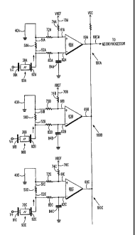
[0019] FIG. 2 shows a fault detection system for a battery charging system for
charging multiple batteries. In FIG. 2, the battery charging system includes a
plurality of resistive elements (e.g., 50A, 50B, and 50C ...), a plurality of
battery
charging stations (e.g., 90A, 90B, and 90C ...), a plurality of comparators
(e.g.,
60A, 60B, and 60C ...), and a microprocessor. A battery charging station
(e.g.,
90B) has a terminal (e.g., 92B) coupled to a common voltage 40 through a
resistive element (e.g., 50B). The battery charging station (e.g., 90B) has
another
terminal (e.g., 91B) coupled to a power source V+. A given comparator (e.g.,
60B) is associated with a corresponding resistive element (e.g., 50B) selected
from the plurality of resistive elements. The given comparator (e.g., 60B) has
a
first input (e.g., 61B) coupled to a first terminal (e.g., 5113) of the
corresponding
resistive element (e.g., 50B) and has a second input (e.g., 62B) coupled to a
CA 02723142 2010-10-27
WO 2009/135111 PCT/US2009/042499
second terminal (e.g., 52B) of the corresponding resistive element (e.g.,
50B).
The first terminal of the given comparator (e.g., 60B) is coupled to a
reference
voltage 70.
[0020] In FIG. 2, each comparator (e.g., 60B) has an output (e.g., 69B) which
generates a voltage transition when the voltage across the corresponding
resistive
element (e.g., 50B) exceeds certain threshold voltage. In one implementation,
the
output (e.g., 69B) of each comparator (e.g., 60B) can be coupled to an
interrupt
input of the microprocessor. In another implementation, the output (e.g., 69B)
of
each comparator (e.g., 60B) can be coupled to a data bus that is configured to
be
polled by the microprocessor. In certain specific implementations, when the
output (e.g., 69B) of each comparator (e.g., 60B) is configured as an open
collector output, the output (e.g., 69B) of the plurality of comparators
(e.g., 60A,
60B, and 60C ...) can be connected together to form one common output 69CM.
The voltage transition on this common output 69CM can be used as an interrupt
signal and can be sent to the interrupt input of the microprocessor directly.
Alternatively, the voltage transition on this common output 69CM can be
latched
as a status bit and such status bit can be polled through a GPIO bus by the
microprocessor running a special high-speed IO monitoring subroutine.
[0021] Once the microprocessor is notified that there a faulty condition in at
least one of the battery charging stations, the microprocessor can evoke the
corresponding service routine or subprogram to handle this faulty condition.
This
service routine or subprogram can perform one of the following implemented
functions. In a first implementation, the microprocessor can disable the power
to
all charging stations (i.e., 90A, 90B, and 90C). In a second implementation,
the
microprocessor can sequentially disable the power to only one charging station
until the faulty one is found; the microprocessor then can disable the faulty
one
from operation and keep all other charging stations in operation condition. In
a
third implementation, the microprocessor can sequentially enable the power to
only one charging station until the faulty one is found; the microprocessor
then
6
CA 02723142 2010-10-27
WO 2009/135111 PCT/US2009/042499
can disable the faulty one from operation and keep all other charging stations
in
operation condition.
[0022] The method and apparatus described above may have one of the following
advantages. It may improve the safety level of battery chargers. It may
protect
certain kind of batteries from incidental damages during charging process.
Additional advantages may be appreciated by people skilled the art.
[0023] In the foregoing specification, specific embodiments have been
described.
However, one of ordinary skill in the art appreciates that various
modifications
and changes can be made without departing from the scope of the invention as
set
forth in the claims below. Accordingly, the specification and figures are to
be
regarded in an illustrative rather than a restrictive sense, and all such
modifications are intended to be included within the scope of present
teachings.
[0024] The benefits, advantages, solutions to problems, and any element(s)
That
may cause any benefit, advantage, or solution to occur or become more
pronounced are not to be construed as a critical, required, or essential
features or
elements of any or all the claims. The invention is defined solely by the
appended
claims including any amendments made during the pendency of this application
and all equivalents of those claims as issued.
[0025] Moreover in this document, relational terms such as first and second,
top
and bottom, and the like may be used solely to distinguish one entity or
action
from another entity or action without necessarily requiring or implying any
actual
such relationship or order between such entities or actions. The terms
"comprises," "comprising," "has", "having," "includes", "including,"
"contains",
"containing" or any other variation thereof, are intended to cover a non-
exclusive
inclusion, such that a process, method, article, or apparatus that comprises,
has,
includes, contains a list of elements does not include only those elements but
may
include other elements not expressly listed or inherent to such process,
method,
article, or apparatus. An element proceeded by "comprises ... a", "has ... a",
"includes ... a", "contains ... a" does not, without more constraints,
preclude the
7
CA 02723142 2010-10-27
WO 2009/135111 PCT/US2009/042499
existence of additional identical elements in the process, method, article, or
apparatus that comprises, has, includes, contains the element. The terms "a"
and
"an" are defined as one or more unless explicitly stated otherwise herein. The
terms "substantially", "essentially", "approximately", "about" or any other
version thereof, are defined as being close to as understood by one of
ordinary
skill in the art, and in one non-limiting embodiment the term is defined to be
within 10%, in another embodiment within 5%, in another embodiment within 1%
and in another embodiment within 0.5%. The term "coupled" as used herein is
defined as connected, although not necessarily directly and not necessarily
mechanically. A device or structure that is "configured" in a certain way is
configured in at least that way, but may also be configured in ways that are
not
listed.
[0026] It will be appreciated that some embodiments may be comprised of one or
more generic or specialized processors (or "processing devices") such as
microprocessors, digital signal processors, customized processors and field
programmable gate arrays (FPGAs) and unique stored program instructions
(including both software and firmware) that control the one or more processors
to
implement, in conjunction with certain non-processor circuits, some, most, or
all
of the functions of the method and/or apparatus described herein.
Alternatively,
some or all functions could be implemented by a state machine that has no
stored
program instructions, or in one or more application specific integrated
circuits
(ASICs), in which each function or some combinations of certain of the
functions
are implemented as custom logic. Of course, a combination of the two
approaches could be used.
[0027] Moreover, an embodiment can be implemented as a computer-readable
storage medium having computer readable code stored thereon for programming a
computer (e.g., comprising a processor) to perform a method as described and
claimed herein. Examples of such computer-readable storage mediums include,
but are not limited to, a hard disk, a CD-ROM, an optical storage device, a
8
CA 02723142 2010-10-27
WO 2009/135111 PCT/US2009/042499
magnetic storage device, a ROM (Read Only Memory), a PROM (Programmable
Read Only Memory), an EPROM (Erasable Programmable Read Only Memory),
an EEPROM (Electrically Erasable Programmable Read Only Memory) and a
Flash memory. Further, it is expected that one of ordinary skill,
notwithstanding
possibly significant effort and many design choices motivated by, for example,
available time, current technology, and economic considerations, when guided
by
the concepts and principles disclosed herein will be readily capable of
generating
such software instructions and programs and ICs with minimal experimentation.
[0028] The Abstract of the Disclosure is provided to allow the reader to
quickly
ascertain the nature of the technical disclosure. It is submitted with the
understanding that it will not be used to interpret or limit the scope or
meaning of
the claims. In addition, in the foregoing Detailed Description, it can be seen
that
various features are grouped together in various embodiments for the purpose
of
streamlining the disclosure. This method of disclosure is not to be
interpreted as
reflecting an intention that the claimed embodiments require more features
than
are expressly recited in each claim. Rather, as the following claims reflect,
inventive subject matter lies in less than all features of a single disclosed
embodiment. Thus the following claims are hereby incorporated into the
Detailed
Description, with each claim standing on its own as a separately claimed
subject
matter.
9