Note: Descriptions are shown in the official language in which they were submitted.
CA 02723419 2010-11-03
53191-15
System for Installation of Photovoltaic Devices on a Structure
This invention was made with U.S. Government support under contract DE-FC36-
07G017054 awarded by the Department of Energy. The U.S. Government has certain
rights in this invention.
FIELD OF THE INVENTION
[001] The present invention relates to an improved photovoltaic device
assembly
and method of making same, more particularly to an improved photovoltaic
device
assembly (kit) with opposing current flows in adjoining rows or columns and
method of
making same for providing solar power.
BACKGROUND
[002] Efforts to improve photovoltaic devices or "PV devices", particularly
to
improve the connection, installation, and service of multiple devices are
subject to
continuing development within the PV industry. Of special interest are those
PV devices
that are integrated into building structures or fascia (e.g. roofing shingles,
exterior wall
surfaces, canopies, awnings), or stand alone PV systems (e.g. solar farms). To
aid in
their commercial and functional viability, they should satisfy a number of
criteria. The
individual devices and the overall assembly (sometimes known as a kit) should
be
robust, that is they should be able to remain functional in a myriad of
environmental
1
CA 02723419 2013-04-16
- 53191-15
conditions (e.g. heat, cold, wind, rain, snow, etc.). In the case of building
structures,
they should also not subject the building structure to overly adverse
modifications due to
their presence, such as multiple roof penetrations made to electrically
connect and/or
locate the plurality of devices, resulting in the roof which could have to be
subsequently
sealed against leaks. The roof penetrations and/or extensive electrical
wiring/connections can make installation time consuming and expensive. In
either a .
building structure or stand alone PV system, the relative ease of installation
provided by
the present invention can be advantageous. Furthermore, when a device
component
(e.g. a single panel and/or a sub-component such as a bypass diode) does
become
, damaged or needs to be replaced, it can be valuable to have a system that
allows easy
replacement of the device component or sub-component
[003] Among the literature that can pertain to this technology include the
following patent documents: .US20080190047(A1); US4321416; US5575861;
US5437735;
US5990414; US6840799; EP1744372; US6875914; US5590495; US5986203;
US2008/0115822;
EP1923920; US7365266; US20070295393 Al; US20070295392 Al; WO 2008/139102,
US2011/0100436, US2011/0183540, W02009/137,348, W02009/137,347,
W02009/137,352, and W02009/137353.
=
SUMMARY OF THE INVENTION
[004] The present invention is directed to a solution to at least one or
more of the issues
described above. Particularly, the present invention seeks to provide a robust
photovoltaic device
assembly and method that can more easily electrically connect a plurality of
PV devices (while
minimizing the total number of electrical connections in the kit) and/or
locate these devices upon a
structure (e.g. a building wall, building roof, or platform). It also can
optionally provide some additional
components (e.g. a spacer piece/device and/or connector pieces) and can
enhance the serviceability
of the device.
2
CA 02723419 2013-04-16 =
- 53191-15
[005] Accordingly, pursuant to a first embodiment of the present invention,
there is
contemplated a photovoltaic device kit including: a. at least a plurality of
photovoltaic
devices in at least a first and a second row or column as applied to a
structure, the
photovoltaic device including: i. a photovoltaic cell assembly including at
least' one
peripheral edge, at least one photovoltaic cell inboard of the at least one
peripheral
edge, which the photovoltaic cell includes a photoactive portion, wherein the
at least one
photovoltaic cell includes a surface that allows transmission of light energy
to the
photoactive portion for conversion into electrical energy; ii. at least one
positive buss
terminal and at least one negative buss terminal for transferring current to
or from the
photovoltaic cell assembly via at least one integral photovoltaic connector
assembly
located within the at least one peripheral edge; and iii. a body portion
including a lower
surface portion that contacts the structure, and an upper surface portion that
receives a
fastener that attaches the photovoltaic device to the structure, wherein the
body portion
is at least partially joined to at least one edge portion of the photovoltaic
cell assembly
along at least a portion of a bottom segment of the body portion while leaving
the
surface of the at least one photovoltaic cell exposed; b. at least one edge
piece disposed
at the end or within the at least upper and adjoining lower row of
photovoltaic devices,
the at least one edge piece including at least one edge connector assembly for
connecting each respective row of photovoltaic devices; wherein, when in use,
a current
flows across the first row or column in one direction and across the second
row or
column in the opposite direction.
[006] Accordingly, pursuant to a second embodiment of the present
invention, there
is contemplated a photovoltaic device assembly including: a. a plurality of
first
photovoltaic devices individually interconnected via a plurality of
photovoltaic device
connector assemblies in a first row, wherein a current flow is created in a
first direction;
b. a plurality of discrete second photovoltaic devices individually
interconnected via the
plurality of photovoltaic device connector assemblies in a second row, wherein
the
current flow is created in an opposing direction from the current flow of the
first
photovoltaic devices; and c. a first edge piece spanning between and
connecting the first
and second rows at one end.
[007] The invention of both the first and/or second embodiments can be
further
characterized by one or any combination of the features described herein, such
as
3
CA 02723419 2010-11-03
WO 2009/137352
PCT/US2009/042522
including at least one spacer device connected between two photovoltaic
devices, one
photovoltaic device and one edge piece, or both; the at least one edge piece
includes a
building connector assembly or electrical lead assembly; the at least one
integral
photovoltaic connector assembly, the at least one edge connector assembly, or
both
include a strain relief feature; the at least one integral photovoltaic
connector assembly,
the at least one edge connector assembly, or both, further includes an
integral connector
housing adapted to receive a connector element; the connector element
comprises: a. a
base portion including a first end portion, a second end portion, an
intermediate portion
and an outer surface; b. a locator portion located on the outer surface of the
intermediate
portion, the locator portion including a bearing wall that is shaped to
generally
complement the integral connector housing; and c. at least one electrically
conductive
member that is substantially surrounded by the base portion and that spans
between the
first and second end portions and includes connective terminals at opposing
ends that
are shaped to interlock with an opposing terminal in the integral connector
housing, so
that the bearing wall partially contacts an opposing surface in the integral
connector
housing; the at least one edge piece includes at least one edge connector
assembly for
connecting to a second edge piece; the at least one edge piece includes an
indicator
device to communicate a circuit status; the structure is a building.
[008] Looking
more towards the second embodiment, it can be further
characterized by one or any combination of the features described herein, such
as
including a second edge piece spanning between and connecting the first and
second
rows at an opposing end, wherein at least the first edge piece includes a
first electrical
circuit that includes at least a pass-though electrical connector or
electrical lead
assembly and wherein at least the second edge piece includes a second
electrical circuit
that includes at least an electrical return circuit interconnect; the
plurality of discrete first
photovoltaic devices and the plurality of discrete second photovoltaic devices
comprise:
a. a photovoltaic cell assembly including at least one peripheral edge, at
least one
photovoltaic cell inboard of the at least one peripheral edge, which the
photovoltaic cell
includes a photoactive portion, wherein the at least one photovoltaic cell
includes a
surface that allows transmission of light energy to the photoactive portion
for conversion
into electrical energy; b. at least one positive buss terminal and at least
one negative
buss terminal for transferring current to or from the photovoltaic cell
assembly via at
4
CA 02723419 2013-04-16
53191-15
least one integral photovoltaic connector assembly located within the at least
one
peripheral edge; and c. a body portion including lower surface portion that
contacts a
structure, and an upper surface portion that receives a fastener that attaches
the
photovoltaic device to the structure, wherein the body portion is at least
partially joined to
at least one edge portion of the photovoltaic cell assembly along at least a
portion of a
bottom segment of the body portion while leaving the surface of the at least
one
photovoltaic cell exposed; the body portion and at least one peripheral edge
at least
include a unitary polymeric portion; the first edge piece and the second edge
piece
comprise a polymeric body that substantially envelops at least a portion of
the first and
second electrical circuits respectfully; the integral photovoltaic connector
assembly
includes a locator feature for locating one of the plurality of discrete first
photovoltaic
devices and the plurality of discrete second photovoltaic devices to another
or to the first
or second end piece within the respective row; the first row, second row, or
both, include
at least one spacer device; the structure is a building.
[009] Accordingly, pursuant to a third embodiment of the present
invention, there is
contemplated a method of constructing a photovoltaic device assembly on a
surface of
a structure, including the steps of: a. providing a plurality of individual
photovoltaic
devices, wherein the individual photovoltaic devices include: i. a
photovoltaic cell
assembly including at least one peripheral edge, at least one photovoltaic
cell inboard of
the at least one peripheral edge, which the photovoltaic cell includes a
photoactive
portion, wherein the at least one photovoltaic cell includes a surface that
allows
transmission of light energy to the photoactive portion for conversion into
electrical
energy; ii. at least one positive buss terminal and at least one negative buss
terminal for
transferring current to or from the photovoltaic cell assembly via at least
one integral
photovoltaic connector assembly located within the at least one peripheral
edae: and iii.
a body portion including a lower surface portion that contacts the structure,
and an upper
surface portion that receives a fastener that attaches the photovoltaic device
to the
structure, wherein the body portion is at least partially joined to at least
one edge portion
of the photovoltaic cell assembly along at least a portion of a bottom segment
of the
body portion while leaving the surface of the at least one photovoltaic cell
exposed; b.
providing a plurality of edge pieces; c. attaching a first individual
photovoltaic device to
the surface; d. attaching a second individual photovoltaic device to the first
individual
CA 02723419 2010-11-03
WO 2009/137352
PCT/US2009/042522
photovoltaic device via a connector element; e. attaching the second
individual
photovoltaic device to the surface; f. repeat steps c-e until a first row is
attached to the
surface, wherein a current flow can flow in a first flow direction; g. begin
attaching a
second row of individual photovoltaic devices adjacent to the first row, using
the same
steps as the first row except that the current flow is in a second flow
direction; and h.
attaching at least one edge piece via a connector element to at least one end
of the first
and second row.
[0010] The
invention of the third embodiment can be further characterized by one or
any combination of the features described herein, such as including the step
of providing
a spacer device; the first row, second row, or both, include at least one
spacer device in
place of at least one of the individual photovoltaic devices; the steps c-h
are repeated to
create the photovoltaic device assembly with a plurality of rows; a separate
connector
element is provided which includes: i. a base portion including a first end
portion, a
second end portion, an intermediate portion and an outer surface; ii. a
locator portion
located on the outer surface of the intermediate portion, the locator portion
including a
bearing wall that is shaped to generally complement the integral connector
housing; and
iii. at least one electrically conductive member that is substantially
surrounded by the
base portion and that spans between the first and second end portions and
includes
connective terminals at opposing ends that are shaped to interlock with an
opposing
terminal in the integral connector housing, so that the bearing wall partially
contacts an
opposing surface in the integral connector housing; some or all of the
plurality of
connector elements have the first end portion integral to the edge piece, the
photovoltaic
device, or both; the structure is a building.
[0011] It is
also should be appreciated that the present invention contemplates a
photovoltaic device assembly and method comprising a plurality of PV devices
of any of
the embodiments described above or subsequently in this application.
[0012] It
should be appreciated that the above referenced embodiments and
examples are non-limiting, as others exist within the present invention, as
shown and
described herein.
6
CA 02723419 2013-04-16
53191-15
DESCRIPTION OF THE DRAWINGS
[0013] FIG. 1 is an exemplary illustration of a perspective view of
an
assembled kit (row) according to an embodiment of the present invention.
[0014] FIG. 1A is an exemplary illustration of a schematic of the one
possible
assembled kit derivation shown in FIG. 1, according to an embodiment of the
present
invention.
[0015] FIG. 2 is another exemplary illustration of a schematic of the
one
possible assembled kit derivation shown in FIG. 1, according to an embodiment
of
the present invention.
[0016] FIG. 3 is a partial exploded view of the bottom two rows (left side)
of the
kit of Figure 2.
[0017] FIG. 4 is one exemplary illustration of an exploded view of a
PV device
piece according to an embodiment of the present invention.
[0018] FIG. 5 is an exemplary illustration of a perspective view of a
connector
piece according to an embodiment of the present invention.
[0019] FIG. 6 is an exemplary illustration of an exploded perspective
view of
two PV devices and the connector of FIG. 5.
[0020] FIG. 7 is an exemplary illustration of a perspective view of a
partially
integrated connector.
[0021] FIG. 8 is an exemplary illustration of a perspective view (top) of
one
possible edge piece according to an embodiment of the present invention.
[0022] FIG. 9 is an exemplary illustration of a perspective view
(bottom) of one
possible edge piece according to an embodiment of the present invention.
7
CA 02723419 2013-04-16
' 53191-15
[0023] FIG. 10 is another exemplary illustration of a perspective
view (bottom)
of an edge piece with ribs and integrated wiring according to an embodiment of
the
present invention.
[0024] FIG. 11 is another exemplary illustration of a perspective
view (bottom)
of an edge piece with ribs and a wiring channel according to an embodiment of
the
present invention.
[0025] FIG. 12 is a perspective view of ribs and wiring channel of
FIG. 11.
[0026] FIG. 13 is an exemplary illustration of a schematic of one
possible kit
derivation according to an embodiment of the present invention.
[0027] FIG. 14 is an exemplary illustration of a row of PV devices with a
spacer
device.
[0028] FIG. 15 is an exemplary illustration of a perspective view of
an
assembled kit (column) according to an embodiment of the present invention.
[0029] FIG. 16 is an exemplary illustration of a schematic of one
possible kit
(column) derivation according to an embodiment of the present invention.
[0030] FIG. 17 is an exemplary illustration of two perspective view
(top and
bottom) of a PV device (column kit) according to an embodiment of the present
invention.
[0031] FIG. 18 is an exemplary illustration of two perspective views
(top and
bottom) of an edge piece (column kit-top) according to an embodiment of the
present
invention.
[0032] FIG. 19 is an exemplary illustration of a perspective view of
a structure
pass-through electrical connector assembly.
8
CA 02723419 2013-04-16
53191-15
DETAILED DESCRIPTION OF THE PREFERRED EMBODIMENT
[0033] The present invention is a photovoltaic device assembly (or
kit) and
method of making same. This assembly can include a plurality of photovoltaic
devices ("PV devices" or "PVD") that are placed in rows or columns (e.g. two
or
more); wherein the devices can be both physically and electrically connected
by
connectors, edge pieces, spacer pieces, or any combination thereof. The
assembly
is configured to aid in providing quick and easy installation and to reduce
the number
of potential structure, (façade or roof ¨ in the case of the preferred
structure of a
building roof application) penetrations needed. Preferably, the photovoltaic
device
assembly utilizes PV devices and connectors that are the same or similar
(functionally and/or structurally) to those described in US patent
applications
publication Nos. 2011/0100436 and 2011/0183540 (and in related W02009/137,348
and W02009/137,347, respectively), and in W02009/137,352 and W02009/137,353.
[0034] Generally, the present invention contemplates a photovoltaic
device
assembly or kit 20 (for example as a row configuration as shown in Figs. 1,
la, and 2
fully assembled and for example as a column configuration fully assembled as
shown
in Fig. 15 and Fig. 16) that can include at least a plurality of PV devices
100 in at
least two rows or columns as applied to a building (or other structure). As
shown in
Fig. 2, the wiring at the bottom of the kit 20 may be routed up and across
(e.g. via
channels 65)
8a
CA 02723419 2010-11-03
WO 2009/137352
PCT/US2009/042522
assembled kit 20 so that the electrical wires are at or near the top of the
kit. The first
row/column configured to produce a current flow 21 (shown with an arrow) in
one
direction and the second row configured to have an opposite current flow. The
kit 20,
can include at least one edge piece 50 located at the end or within the at
least two
rows/columns of PV devices 100. The PV devices 100 can be further described as
at
least including a photovoltaic cell assembly 110 and a body portion 120.
[0035] The edge
piece 50 may include two or more edge connector assemblies 52
for connecting each respective row or column of photovoltaic devices. The edge
piece
can include electrical element or elements 51 incorporated between edge
connector
assemblies 52 such that the rows are electrically connected together or have a
single
electrical output 500 from the kit 20 at or near an outer edge of the kit. In
certain cases,
the edge piece may have no electrical connector assemblies 52 and function
solely as a
filler piece 54 or a starter piece 53. Preferably, the edge connector
assemblies and the
photovoltaic device connector assemblies 58 are the same or similar (e.g.
functionally
and/or structurally). A description for one is intended to apply to the other
unless
specifically stated otherwise. The edge piece connector assembly can be, as in
the first
embodiment, integral to the edge piece (i.e. located within at least one
peripheral edge
of an edge piece as is shown in Fig. 3) or it can be a separate element that
is used in the
assembly between one peripheral edge of an edge piece and one peripheral edge
of a
PV device or between peripheral edges of adjacent edge pieces and mating to
the
connector housing or connector elements in those pieces, depending on the kit
design.
[0036] The edge
piece connector assembly 52 can include a housing 56 integral to
the edge piece (e.g. a female housing), as shown in the PV device in Fig 6,
adapted to
receive a separate connector piece 58 (i.e., shaped to generally complement an
opposing connector housing), a connector integrated housing 59 with a
connector piece
at least partially integrated therein (Fig 7), or any combination thereof and
at least one
electrically conductive member that spans between the first and second end
portions
and includes connective terminals at opposing ends that are shaped to
interlock with an
opposing terminal in the opposing connector housing..
[0037] The
assembly can also include any number of spacer pieces 400 (e.g. as
shown in Fig. 14) that may or may not contain any photovoltaic devices (e.g.
power
generating means) or other components. It is contemplated that spacer pieces
can
9
CA 02723419 2010-11-03
WO 2009/137352
PCT/US2009/042522
provide additional functionality to the kit. In one example, a spacer piece
400 can
provide a through hole for roof vents. In another example, a spacer piece 400
or pieces
can provide an aesthetic function, such as staggering the rows or columns.
[0038] It is
also contemplated that the assembly or kit can be configured to provide a
targeted power output (e.g. 0.1 to 8 KWp or more (1<1.Np defined as kilowatt-
peak) and to
fit standard building designs (e.g. mass produced homes) that share roof
and/or fascia
layouts, or can be custom configured for one-off designs. For example, the kit
can be
configured to fit (e.g. number of PV devices, number of rows, number and
location of
spacers/edge pieces) one particular roof design that is utilized in a
particular model
home offered by a builder (e.g. the BeaumontTM model offered by Pulte Homes
TM)
[0039] The
individual components that make up the kit are described in further detail
and illustrative examples of some of the possible kit configurations are
provided below.
PV DEVICE
[0040] In an
illustrative example, the PV device 100 can be described generally as a
three dimensional article that includes an energy producing device (e.g. solar
cells),
electrical circuitry to transfer the energy produced, and a body which holds
the energy
producing device and allows it to be effectively mounted onto a structure. It
is
contemplated that a PV device 100 of the present invention is preferably a
discrete part
/component that is used in the overall kit. It is also contemplated that the
PV devices
used in one row/column are configured to have a current flow 21 in one
direction and the
PV devices used in an adjoining or second row/column are configured to have a
current
flow 21 in an opposing direction. It may also be described that the PV devices
of one
row/column have one polarity while the PV devices of the second row/column
have an
opposite polarity.
[0041] For
example, as shown in Fig. 3, the PV device 100 can be further described
as including a photovoltaic cell assembly 110 and a body portion 120 (which
can also be
referred to as a body support portion where it provides structural support).
The body
portion 120 having an upper surface portion 122, a lower surface portion 124
and side
wall portion 126 spanning therebetween. The body portion 120 can be further
described
as including a main body portion 222, a side body portion 224, and an optional
bottom
body portion 226 and locator (not shown). The PV device 100 can also be
described as
CA 02723419 2010-11-03
WO 2009/137352
PCT/US2009/042522
having an active portion 130 and an inactive portion 135. The active portion
130 can
include at least the photovoltaic cell assembly 110, a portion of the side
body portion 224
and the optional bottom body portion 226. The inactive portion 135 can include
at least
the main body portion 222, a portion of the side body portion 224, and some or
all of the
electrical circuitry of the PV device 100.
[0042] For
example as shown in an exploded view of a PV device 100 in Fig. 4, the
photovoltaic cell assembly 110 can be further described as including a
photovoltaic cell
111, protective layers 113, and at least some of the electrical circuitry 114
of the PV
device. The PV devices 100 can also be described in an alternative fashion.
The PV
devices 100 can include components such as the photovoltaic cell assembly 110,
at
least one positive buss terminal 140 and at least one negative buss terminal
141(not
shown), and a body portion 120.
[0043] The PV
devices 100 can include at least one peripheral edge 112, at least
one photovoltaic cell 111 inboard of the at least one peripheral edge 112.
[0044] The
positive and negative buss terminals 140, 141, which can function to
transfer current to or from the photovoltaic cell assembly 110 via at least
one integral
photovoltaic connector assembly 57 located within the at least one peripheral
edge 112.
Preferably, the positive and negative buss terminals 140, 141 are located on
opposing
edges of the PV device and each transfer current via an integral connector
assembly 57
disposed in opposing peripheral edges. For example, the PV device used in the
first row
have the positive buss terminal 140 on the right side of the PV device and the
negative
buss terminal 141 on the left side, in the second row this is reversed. In the
case of a
column, the positive buss terminal 140 is on top and the negative on the
bottom for the
first column and reversed on the adjoining column.
[0045] The body
portion 120 lower surface portion 124 can contact the structure
(e.g. building substrate and/or structure). Also having an upper surface
portion 122 that
receive a fastener (not shown, e.g. nail, screw, staple, rivet, etc.) that
attaches the
photovoltaic device 100 to the structure. Furthermore, the body portion 120
can be at
least partially joined to at least one edge portion of the photovoltaic cell
assembly 110
along at least a portion of a bottom segment 156 of the body portion 120 while
leaving at
least a portion of the at least one photovoltaic cell 111 exposed to receive
radiation.
11
CA 02723419 2010-11-03
WO 2009/137352
PCT/US2009/042522
[0046] It is
contemplated that the PV device 100 can be constructed at least partially
of flexible materials (e.g. thin films or deformable materials, with
significant plastic or
elastic elongation such as plastics, synthetic and natural rubbers, films,
elastomers, or
the like) to allow at least some flexibility for conforming to an irregular
contour in a
building structure. It is also contemplated that it can be desirable to at
least keep the
photovoltaic cell relatively rigid, generally to prevent any cracking of the
cell. Thus,
some parts of the PV device can be constructed with a more rigid material
(e.g. glass
plate, mineral filled composites, or polymeric sheets). Although, the
photovoltaic cell can
be partially or substantially rigid, it is possible for the PV device to be
generally flexible.
For this invention, flexible means that the PV device is more flexible or less
rigid than the
substrate (e.g. structure) to which it is attached. Preferably, in the case of
a flexible
substrate the PV device can bend about a 1 meter diameter cylinder without a
decrease
in performance or critical damage. Preferably, in the case of a rigid
substrate the PV
device can bend about 20 meter diameter cylinder without a decrease in
performance or
critical damage. For example, in the case of a PV device shingle, shingles
generally are
less rigid than the roof deck; the roof deck provides structural rigidity. In
some other
examples the roofing product itself provides the necessary rigidity and the
roof deck is
absent, or minimized.
The photovoltaic cell 110, contemplated in the present invention may be
constructed of
any number of known photovoltaic cells commercially available or may be
selected from
some future developed photovoltaic cells. These cells function to translate
light energy
into electricity. The photoactive portion of the photovoltaic cell is the
material which
converts light energy to electrical energy. Any material known to provide that
function
may be used including crystalline silicon, or amorphous silicon. However, the
photoactive layer is preferably a layer of IB-IIIA-chalcogenide, such as IB-
IIIA-selenides,
IB-IIIA-sulfides, or IB-IIIA-selenide sulfides. More specific examples include
copper
indium selenides, copper indium gallium selenides, copper gallium selenides,
copper
indium sulfides, copper indium gallium sulfides, copper gallium selenides,
copper indium
sulfide selenides, copper gallium sulfide selenides, and copper indium gallium
sulfide
selenides (all of which are referred to herein as CIGSS). These can also be
represented
by the formula Culn(1-x)GaxSe(2-y)Sy where x is 0 to 1 and y is 0 to 2. The
copper
indium selenides and copper indium gallium selenides are preferred. Additional
12
CA 02723419 2010-11-03
53191-15
electroactive layers such as one or more of emitter (buffer) layers,
conductive layers
(e.g. transparent conductive layers) and the like as is known in the art to be
useful in
CIGSS based cells are also contemplated herein. These cells may be flexible or
rigid
and come in a variety of shapes and sizes, but generally are fragile and
subject to
environmental degradation. In a preferred embodiment, the photovoltaic cell
assembly
110 is a cell that can bend without substantial cracking and/or without
significant loss of
functionality. Exemplary photovoltaic cells are taught and described in a
number of US
patents and publications, including US3767471, US4465575, US20050011550 Al,
EP841706 A2, US20070256734 al, EP1032051A2, JP2216874, JP2143468, and
JP10189924a.
CONNECTOR
[0047] It is contemplated that the kit 20 may use a plurality of connectors
58, for
example such as those described in US provisional application 61/098,941.
These connectors can be separate components (e.g. as
shown in Figs. 5-6) or partially integrated into the PV device 100, the edge
piece 50, or
both (e.g. as shown in Fig. 7). In an illustrative example shown in Fig. 5,
the connector
58 can be described generally as including a base portion 210 including a
first end
portion 212, a second end portion 214 and an outer surface 216. It also can
include a
locator portion 218 located on the outer surface. In one particular
embodiment, the-
locator portion can be described as including a bearing wall that can be
shaped to
generally complement an opposing female connector housing 56 that can be
located in a
PV device 100 or edge piece 50. Furthermore, upon installation, the bearing
wall can at
least partially contact an opposing surface in the female connector housing.
Moreover,
the connector assembly can include at least one electrically conductive member
that is
substantially surrounded by the base portion and that spans between the first
and
second end portions and includes connective terminals at opposing ends. These
terminals can be shaped to interlock with an opposing terminal in the opposing
female
connector housing.
[0048] It is also contemplated that the opposing female connector housing
can be
integral to an outer wall section (e.g. portions such as top, bottom, or sides
of the PV
device or edge piece) of the PV device 100 or edge piece 50. The housing can
be
connected to the PV device or edge piece via a fastener scheme (e.g.
mechanical
13
CA 02723419 2010-11-03
WO 2009/137352
PCT/US2009/042522
fasteners, adhesives, or a combination thereof) or can be integrated into the
PV device
or edge piece via the structure of the device/piece (e.g. over-molded into the
device or
part of the framework of the PV device or edge piece for example as shown in
Fig 10).
In either case, it is contemplated that female connector housing integral to
or connected
to a PV device or edge piece and/or the connector assembly includes a strain
relief
feature (or combination of one or more features) to allow movement of the
assembly
while maintaining an electrical contact between the respective terminals.
[0049] The edge
piece connector assembly may be further characterized by one or
any combination of the features described herein, such as the opposing female
connector housing is integral to an outer wall section of the edge piece or
the
photovoltaic device; the connector assembly includes a bypass diode
electrically
connected to the at least one electrically conductive member; the connector
assembly
includes an indicator device to communicate a circuit status; the connector
assembly
includes a locking device that locks the male connector element to the
opposing female
connector housing upon installation; the connector assembly includes a second
electrically conductive member, the first end portion of which is integral to
the outer wall
section of the photovoltaic device or edge piece, the connector element (male
or female)
is integral to the first connector housing (male or female), an outwardly
projecting portion
in the locator portion that projects upward towards a top surface that is
generally
coplanar with a top surface of the photovoltaic device or edge piece.
[0050] It
should be appreciated that the above referenced aspects and examples are
non-limiting, as others exist within the present invention, as shown and
described herein.
EDGE PIECE
[0051] The edge
piece 50, for example as shown in Figs.8-11 and 18, generally
function to physically and/or electrically connect at least two rows or
columns of PV
devices 100. It can also function to connect one edge piece to another edge
piece. The
edge piece 50 can be disposed at a single end, opposing ends, within a
row/column, or
any combination thereof of a row/column of PV devices 100. It is contemplated
that an
edge piece 50 can include a through roof (or building structure) connector
feature (e.g. a
structure pass-through electrical connector assembly 510) or electrical leads
or insulated
wires (e.g. electrical lead assembly) that allow for the electrical output of
the PV device
14
CA 02723419 2010-11-03
WO 2009/137352
PCT/US2009/042522
or devices to be electrically connected to the complimentary electrical
devices located
within the structure. It is also contemplated that a filler piece 54 may be
used to fill any
possible gaps in the edge pieces when assembled. The edge piece can be
attached to
the structure in the same manner as the PV device 100, for example with a
fastener
such as a nail or screw being driven through a portion of the body. The
fastener
preferably being placed in an area that does not contain any additional
components (e.g.
wires, connectors and the like). It is contemplated that a fastening zone (not
shown) can
be marked on the edge piece to aid in installation (e.g. physical markings on
the PV
device, edge piece, or both such as "nail here" or "fastener" or some other
graphical
demarcation). The edge piece 50 can also include additional components such as
electrical transmission lines (e.g. wires), electrical switches, fuses, by-
pass diodes, solar
cells, circuit status indicators, or any combination thereof.
[0052] As shown
in Figs. 8-13, it is contemplated that the main body portion 60 can
have an outer surface portion 62, an inner surface portion 64 (e.g. portion
that contacts
the building or structure surface) and side surface portions 66 that connect
the outer and
inner surface portions 62, 64. Optionally, the inner surface portion 64 can be
solid (e.g.
a unitary block) or have geometric features (e.g. ribs 61 for example as shown
in Fig 10).
The main body portion 60 can be any number of shapes or sizes, but preferably
is
shaped to complement the shape of the PV device 100 that it connects thereto.
In this
example, the main body portion 60 is "stepped" vertically to allow for a
complementary fit
to two rows of PV devices that are stacked and layered (e.g. akin to roofing
shingles).
The main body portion 60 can also be "staggered" horizontally to allow for a
complimentary fit to the two rows of PV devices, if the devices are installed
with an offset
(again, akin to roofing shingles). It also can include a flashing portion 68
that can be
adapted to interface with and/or sit under other building materials (e.g.
abutting standard
roofing shingles, trim materials, building siding, or the like).
[0053] In one
illustrative example, shown in Fig. 9, a bottom view of an edge piece
50 can be described generally as including a main body portion 60 and two edge
connector assembly 52 (one example of which may be "the partially integrated
connector
assembly" as described above) and an electrical element or elements 51 (e.g.
wires,
electrically conductive foil or polymers) spanning between the two edge
connector
assemblies 52, one of which is hidden behind the body portion 60 of the edge
piece.
CA 02723419 2010-11-03
WO 2009/137352
PCT/US2009/042522
[0054] In
another illustrative example shown in Fig. 10, (an alternative bottom view
of an edge piece) the electrical element 51 can be integrally connected to the
edge piece
50 (e.g. molded within the piece). Preferably, the element is wire or foil
pieces that are
molded into the edge piece 50 (partially or fully encapsulated by the edge
piece) along
with at least a portion of the connector assembly 52.
[0066] In yet
another illustrative example, shown in Figs 11-12 (also bottom views of
the edge piece), the electrical element 51 can be removably attached via any
number of
attachment features (e.g. adhesive, mechanical fasteners, press-fit into
channels 65, for
example, cut into ribs 61, shown in Fig 12, or any combination thereof). It is
contemplated that the PV devices 100 may also include ribs 61 with channels 65
for any
required wire routing.
[0056] The main
body portion 60 can be constructed of any number of materials
(e.g. polymers, metals and/or ceramics), so long as it resists environmental
degradation
as it is exposed to the outdoor over the years of service (e.g. 10, 20 or 30
years or
more). Preferred materials or combinations of materials include a filled or
unfilled
moldable plastic (e.g. polyolefins, acrylonitrile butadiene styrene,
hydrogenated styrene
butadiene rubbers, polyester amides, polysulfone, acetel, acrylic, polyvinyl
chloride,
nylon, polyethylene terephthalate, polycarbonate, thermoplastic and thermoset
polyurethanes, synthetic and natural rubbers, epoxies, styrene-acrylonitrile
("SAN"),
polymethyl methacrylate, polystyrene, or any combination thereof). Fillers can
include
one or more of the following: colorants, fire retardant ("FR") or ignition
resistant ("IR")
materials, reinforcing materials, such as glass or mineral fibers, surface
modifiers.
Plastic can also include anti-oxidants, release agents, blowing agents, and
other
common plastic additives.
ILLUSTRATIVE EXAMPLES
[0067] The
various examples discussed below and shown in the figures generally
attempt to take PV devices, edge pieces, connectors and optionally other
components
(e.g. spacers 400 as shown in Fig. 14) to create a photovoltaic device kit 20
that when
assembled can be configured to provide a targeted power output and preferably
require
two or less electrical connections to the inverter or the underlying building
electrical
system. It is contemplated that the geometry of these kits can be varied and
the
16
CA 02723419 2010-11-03
WO 2009/137352
PCT/US2009/042522
following examples should not be considered as limiting. Thus, for the sake of
clarity, the
following examples are provided to illustrate the invention but are not
intended to limit
the scope thereof. The rows of PV devices can be staggered (e.g. as
traditional roofing
shingles) or lined up in columns. The rows and/or columns can be vertical,
horizontal or
anywhere in-between. In all the illustrative examples discussed below, it is
assumed
that the PV devices can be physically and electrically connected to one
another within
the row via connector assemblies as described previously. The lines 600 shown
represent the electrical transmission line or circuits within the PV devices
100 and/or the
edge pieces 50 and the dots represent connectors.
[0058]
Referring to Fig. 13, a first illustrative example of the present invention is
shown (schematical view). In example, a photovoltaic device kit 20 can include
at least
a plurality of PV devices 100 in multiple rows and multiple edge pieces 50
(one set on
each row end). At both ends of a row of PV devices 100, the PV devices can be
physically and electrically connected to an edge piece 50 via and edge piece
connector
assembly 52. The edge piece can include electrical element or elements 51 that
electrically connect the rows together and have two electrical outputs 500
from the kit 20
at or near an inner edge of the kit.
[0059] It is
contemplated that the electrical output 500 may be accomplished via a
pass-through electrical connector assembly 510 (for example as shown in Fig.
19 as a
part of a connector assembly) or electrical lead assembly (for example a set
of wires
attached to an edge piece or a connector assembly ¨ not shown)
[0060]
Referring to Fig. 14, a single row of PV devices 100 including an exemplary
spacer piece 400 is shown.
[0061]
According to another embodiment, tile style installations (e.g. columns) are
preferably arranged as shown in Figs. 15 and 16. Referring to Figs. 15 - 18, a
second
illustrative example of the present invention is shown. In this example, one
possible
vertical configuration of PV devices 100 is shown (e.g. 2 rows x 3 columns).
In this
example 3 columns of PV devices 100 include a flow channel 1100 on one side
that can
aid in water flow control and/or provide an interlocking function. Also, edge
pieces 50
are provided with geometry appropriate to fit in this vertical configuration
and with
different geometries between edge pieces at the top of the column versus the
bottom of
the column (e.g. as seen in Fig. 18). The fully assembled kit 20 is shown in
Figs. 15 and
17
CA 02723419 2010-11-03
WO 2009/137352
PCT/US2009/042522
16. Also shown in this example are ribs 61 that are formed on the back side of
the PV
devices and edge pieces. These ribs 61 can help reduce the mass of the
components
and aid in providing the desired rigidity for the components. Rib designs can
be
incorporated into both the vertical (column) and horizontal (row) examples or
embodiments.
[0062] In Fig.
16, a schematic of one possible electrical circuit is shown with
connectors 52 and electrical element 51 (wiring preferably integral to the PV
devices and
edge pieces. In the
vertical configuration of the kit 20, the physical and electrical
connections to the PV devices 100 occur at or near the top and bottom of the
devices
(versus at the sides as in the row configurations described in the earlier
examples).
[0063] Unless
stated otherwise, dimensions and geometries of the various structures
depicted herein are not intended to be restrictive of the invention, and other
dimensions
or geometries are possible. Plural structural components can be provided by a
single
integrated structure. Alternatively, a single integrated structure might be
divided into
separate plural components. In addition, while a feature of the present
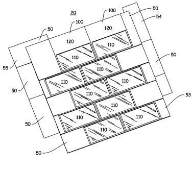
invention can
have been described in the context of only one of the illustrated embodiments,
such
feature can be combined with one or more other features of other embodiments,
for any
given application. It will also be appreciated from the above that the
fabrication of the
unique structures herein and the operation thereof also constitute methods in
accordance with the present invention.
[0064] The
preferred embodiment of the present invention has been disclosed. A
person of ordinary skill in the art would realize however, that certain
modifications would
come within the teachings of this invention. Therefore, the following claims
should be
studied to determine the true scope and content of the invention.
[0065] Any
numerical values recited in the above application include all values from
the lower value to the upper value in increments of one unit provided that
there is a
separation of at least 2 units between any lower value and any higher value.
As an
example, if it is stated that the amount of a component or a value of a
process variable
such as, for example, temperature, pressure, time and the like is, for
example, from 1 to
90, preferably from 20 to 80, more preferably from 30 to 70, it is intended
that values
such as 15 to 85, 22 to 68, 43 to 51, 30 to 32 etc. are expressly enumerated
in this
specification. For values which are less than one, one unit is considered to
be 0.0001,
18
CA 02723419 2010-11-03
53191-15
0.001, 0.01 or 0.1 as appropriate. These are only examples of what is
specifically
intended and all possible combinations of numerical values between the lowest
value
and the highest value enumerated are to be considered to be expressly stated
in this
application in a similar manner.
[0066] Unless otherwise stated, all ranges include both endpoints and all
numbers
between the endpoints. The use of "about" or "approximately" in connection
with a range
applies to both ends of the range. Thus, "about 20 to 30" is intended to cover
"about 20
to about 30", inclusive of at least the specified endpoints.
[0068] The term "consisting essentially or to describe a combination shall
include
the elements, ingredients, components or steps identified, and such other
elements
ingredients, components or steps that do not materially affect the basic and
novel
characteristics of the combination.
[0069] The use of the terms "comprising" or "including" to describe
combinations of
elements, ingredients, components or steps herein also contemplates
embodiments that
consist essentially of the elements, ingredients, components or steps.
[0070] Plural elements, ingredients, components or steps can be provided by
a
single integrated element, ingredient, component or step. Alternatively, a
single
integrated element, ingredient, component or step might be divided into
separate plural
elements, ingredients, components or steps. The disclosure of "a" or "one" to
describe
an element, ingredient, component or step is not intended to foreclose
additional
elements, ingredients, components or steps.
ELEMENT NUMBER TABLE
photovoltaic device assembly or kit 20
current flow 21
edge piece 50
electrical element of the edge piece 51
edge connector assemblies 52
starter piece 53
filler piece 54
end piece 55
female connector housing 56
separate connector piece 58
integral photovoltaic connector assembly 57
19
CA 02723419 2010-11-03
WO 2009/137352
PCT/US2009/042522
male connector housing 59
main body portion 60
ribs 61
outer surface portion 62
inner surface portion 64
channels 65
side surface portions 66
flashing portion 68
photovoltaic device(s) 100
photovoltaic cell assembly 110
a photovoltaic cell 111
peripheral edge 112
protective layers 113
electrical circuitry 114
body portion 120
upper surface portion 122
lower surface portion 124
side wall portion 126
active portion 130
inactive portion 135
positive buss terminal 140
negative buss terminal 141
bottom segment 156
base portion 210
first end portion 212
second end portion 214
outer surface 216
locator portion 218
main body portion 222
side body portion 224
body portion 226
spacer piece 400
electrical output 500
pass-through electrical connector assembly 510
electrical transmission lines in PV device 600
flow channel 1100