Note: Descriptions are shown in the official language in which they were submitted.
CA 02723428 2010-11-03
WO 2009/149014
PCT/US2009/045843
HIGH RESISTIVITY METAL FAN OUT
Field of the Invention
[0001] This relates generally to the formation of metal traces on
substrates,
and more particularly, to the formation of metal traces in the border areas of
a touch
sensor panel in a manner that allows for higher resistivity conductive
materials to be
used to improve trace reliability, reduce noise, and lower manufacturing
costs.
Background of the Invention
[0002] Many types of input devices are presently available for
performing
operations in a computing system, such as buttons or keys, mice, trackballs,
joysticks, touch sensor panels, touch screens and the like. Touch screens, in
particular, are becoming increasingly popular because of their ease and
versatility of
operation as well as their declining price. Touch screens can include a touch
sensor
panel, which can be a clear panel with a touch-sensitive surface, and a
display
device such as a liquid crystal display (LCD) that can be positioned partially
or fully
behind the panel so that the touch-sensitive surface can cover at least a
portion of the
viewable area of the display device. Touch screens can allow a user to perform
various functions by touching the touch sensor panel using a finger, stylus or
other
object at a location dictated by a user interface (UI) being displayed by the
display
device. In general, touch screens can recognize a touch event and the position
of the
touch event on the touch sensor panel, and the computing system can then
interpret
the touch event in accordance with the display appearing at the time of the
touch
event, and thereafter can perform one or more actions based on the touch
event.
[0003] Mutual capacitance touch sensor panels can be formed from a
matrix
of drive and sense lines of a substantially transparent conductive material
such as
Indium Tin Oxide (ITO), often arranged in rows and columns in horizontal and
vertical directions on a substantially transparent substrate. In some touch
sensor
panel designs, the substantially transparent drive and/or sense lines can be
routed to
one edge of the substrate for off-board connections using metal traces in the
border
la-1027201 1
CA 02723428 2010-11-03
WO 2009/149014
PCT/US2009/045843
areas of the substrate where transparency may not be required. Because these
metal
traces are thin, low resistance conductive material may be needed. To create
such
traces, multiple layers of conductive material may be needed to adhere low
resistance material to the substrate and form the traces. However, the
processing of
multiple layers can increase manufacturing costs. In addition, there can be
reliability issues involved in the fabrication of stackups of these thin metal
layers.
Furthermore, these thin metal traces do not provide maximum shielding from
noise
sources such as the LCD.
= Summary of the Invention
[0004] This relates to the formation of metal traces in the border areas of
a
touch sensor panel to provide improved reliability, better noise rejection,
and lower
manufacturing costs. The metal traces can be coupled to rows on the touch
sensor
panel in an interleaved manner, so that any two successive rows can be coupled
to
metal traces in border areas on opposite sides of the touch sensor panel. In
addition,
by utilizing the full width available in the border areas in some embodiments,
the
metal traces can be formed from higher resistivity metal, which can reduce
manufacturing costs and improve trace reliability. The wider traces can also
provide
better noise immunity from noise sources such as an LCD by providing a larger
fixed-potential surface area and by more effectively coupling the drive lines
to the
fixed potential.
[0005] By making the metal traces fill up the available width of the
border
areas, the traces can be wider and thus the overall line resistance of the
trace can be
lower, or the resistivity of the material can be increased for the same
overall line
resistance. For example, a single thicker and wider layer of
Molybdenum/Niobium
(Mo/Nb) having a thickness of about 3000-5000 A can be formed on a substrate.
The higher resistivity of Mo/Nb is compensated for by the increased width and
height of the Mo/Nb layer. After the Mo/Nb layer is deposited at the preferred
thickness, it can be patterned (etched) to form traces. A layer of conductive
material
such as ITO can then be formed over the Mo/Nb layer. A conductive material
layer
can then be patterned to form the drive or sense lines that couple to the
metal traces,
and can also be patterned over the Mo/Nb traces to form another protective
layer for
la-1027201 2
CA 02723428 2013-09-13
the MoiNb traces. A protective layer of material such as silicon oxide (Si02)
can then
be formed over the Mo/1\lb layer and the conductive material layer.
[0006] In general, the ability to use higher resistivity material
enables more
flexibility in the material stack. For example, in two conductive layer
embodiments,
manufacturing costs can be reduced as compared to three-layer stackups of
thin,
higher conductivity material. The fewer number of conductive layers also
reduces the
problem of side wall control present in when multi-layer stackups are
patterned. In
addition, the wider, thicker traces are generally of higher reliability,
because etching
defects, corrosion or other environmental effects may not create problems as
easily as
if the traces were thinner.
[0007] Although the embodiments described above utilize higher
resistivity
conductive material, such material need not be used. If low resistivity
material is used
to form the wide traces, the line resistance can be made even lower. This
reduced line
resistance can produce a better coupling to ground (or some fixed potential)
for the
wide row traces, improving the noise shielding effectiveness of the rows.
Alternatively, a low resistance material can be used with the traces widths
kept thin.
The thin metal traces can enable a reduction in the width of the touch sensor
panel.
For example, a thinned three-layer stackup including low resistance material
can be
used, and in some cases may be less expensive than to develop an alternate
chemistry
two-layer stackup.
[0007A] Accordingly, in one aspect the present invention provides a
method of
forming conductive traces on a touch sensor panel, comprising: forming and
patterning a stackup of a first conductive material over a substrate in one or
more
border areas of the touch sensor panel to create one or more traces such that
the one or
more traces are electrically isolated from one another and occupy
substantially a full
area of ef the border area, wherein at least one trace has varying width along
the
length of the trace; and forming and patterning a layer of a second conductive
material
over the substrate to create one or more rows, each row coupled to a different
trace,
the rows forming part of a plurality of sensors on the touch sensor panel.
[0007B] In a further aspect, the present invention provides a method of
fabricating conductive traces on a touch sensor panel, comprising: routing
rows on the
touch sensor panel to an edge of the touch sensor panel using conductive
traces
3
CA 02723428 2013-09-13
-
formed in one or more border areas of the touch sensor panel, the traces
configured
such that the conductive traces are electrically isolated from one another and
occupy
substantially a full area of the border areas to enable a single layer of
conductive
material to be used for the conductive traces, wherein at least one trace has
varying
-- width along the length of the trace.
[0007C] In a further aspect, the present invention provides a method
for routing
a portion of a plurality of sensors in a touch sensor panel to a single edge
of the touch
sensor panel with higher reliability, comprising: forming and patterning a
stackup of
conductive material into traces in one or more border areas of the touch
sensor panel,
-- the traces coupled to the portion of the plurality of sensors and
configured such that
the traces are electrically isolated from one another and occupy substantially
a full
area of the border areas, wherein at least one trace has varying width along
the length
of the trace.
[0007D] In a further aspect, the present invention provides a touch
sensor panel
-- comprising high reliability conductive traces for routing a portion of a
plurality of
sensors in a touch sensor panel to a single edge of the touch sensor panel,
comprising:
a stackup of a first conductive material patterned into traces in a border
area of the
touch sensor panel, the traces configured such that the traces are
electrically isolated
from one another and te occupy substantially a full area of the border area,
wherein at
-- least one trace has varying width along the length of the trace; and a
second
conductive material patterned to create one or more rows, each row coupled to
a
different trace, the rows forming the portion of the plurality of sensors to
be routed to
the single edge of the touch sensor panel.
Brief Description of the Drawings
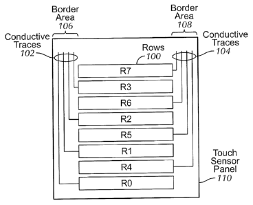
[0008] FIG. lA illustrates a top view of row traces representing either
drive or
sense lines and metal traces represented symbolically as thin lines in border
areas of a
touch sensor panel according to embodiments of the invention.
[0009] FIG. 1B illustrates the exemplary touch sensor panel of FIG.
1A, with
metal traces drawn with representative widths (not to scale) according to
-- embodiments of the invention.
[0010] FIG. IC illustrates a close up view of an exemplary location
of a
border area at which a transition from six to seven metal traces is occurring
according
to embodiments of the invention.
3a
CA 02723428 2010-11-03
WO 2009/149014
PCT/US2009/045843
[0011] FIG. 2A illustrates an exemplary stackup of higher resistivity
material that can be used to form wide traces in the border areas of a touch
sensor
panel according to embodiments of the invention.
[0012] FIG. 2B illustrates an exemplary stackup of low resistivity
material
that can be used to form thinned traces in the border areas of a touch sensor
panel
according to embodiments of the invention.
[0013] FIG. 3 illustrates an exemplary double-sided ITO (DITO) touch
sensor panel having wide conductive traces in the border areas of the touch
sensor
panel according to embodiments of the invention.
[0014] FIG. 4 illustrates an exemplary computing system including a touch
sensor panel utilizing improved metal traces in the border areas according to
embodiments of the invention.
[0015] FIG. 5A illustrates an exemplary mobile telephone having a
touch
sensor panel that includes improved metal traces in the border areas according
to
embodiments of the invention.
[0016] FIG. 5B illustrates an exemplary digital media player having a
touch
sensor panel that includes improved traces in the border areas according to
embodiments of the invention.
Detailed Description of the Preferred Embodiments
[0017] In the following description of preferred embodiments, reference is
made to the accompanying drawings which form a part hereof, and in which it is
shown by way of illustration specific embodiments in which the invention can
be
practiced. It is to be understood that other embodiments can be used and
structural
changes can be made without departing from the scope of the embodiments of
this
invention.
[0018] This relates to the formation of metal traces in the border
areas of a
touch sensor panel to provide improved reliability, better noise rejection,
and lower
manufacturing costs. The metal traces can be coupled to rows on the touch
sensor
panel in an interleaved manner, so that any two successive rows can be coupled
to
metal traces in border areas on opposite sides of the touch sensor panel. In
addition,
la-1027201 4
CA 02723428 2010-11-03
WO 2009/149014
PCT/US2009/045843
by utilizing the full width available in the border areas, the metal traces
can be
formed from higher resistivity metal, which can reduce manufacturing costs and
improve trace reliability. The wider traces can also provide better noise
immunity
from noise sources such as an LCD by providing a larger fixed-potential
surface area
and by more effectively coupling the drive lines to the fixed potential.
[0019] Although embodiments of the invention may be described and
illustrated herein in terms of mutual capacitance touch sensor panels, it
should be
understood that embodiments of this invention are not so limited, but are
additionally applicable to self-capacitance sensor panels, and both single and
multi-
touch sensor panels in which the fabrication of metal traces in the border
areas of a
touch sensor panel is required. Furthermore, although embodiments of the
invention
may be described and illustrated herein in terms of double-sided ITO (DITO)
touch
sensor panels, it should be understood that embodiments of the invention are
also
applicable to other touch sensor panel configurations, such as configurations
in
which the drive and sense lines are formed on different substrates or on the
back of a
cover glass, configurations in which the drive and sense lines are formed on
the
same side of a single substrate, and configurations in which the drive and
sense lines
are formed in geometries other than rows and columns.
[0020] FIG. lA illustrates a top view of row traces (R0-R7) 100
representing
either drive or sense lines, and conductive traces 102 and 104 represented
symbolically as thin lines in border areas 106 and 108 of touch sensor panel
110
according to embodiments of the invention. To make full use of the length of
border
areas 106 and 108, in some embodiments row traces 100 can be coupled to metal
traces 102 and 104 in an interleaved manner as shown in FIG. 1A, which results
in
some metal traces running the full length of touch sensor panel 110. However,
in
alternative embodiments, interleaving need not be employed, and the metal
traces
can be routed in either or both of the border areas on either side of the
touch sensor
panel. In the example of FIG. 1A, rows RO, R1, R2 and R3 are coupled to metal
traces 102 in left border area 106, while interleaved rows R4, RS, R6 and R7
are
coupled to metal traces 104 in right border area 108. Note that the row
designations
R0-R7 in FIG. lA are merely exemplary, and that other row designations (such
as
sequentially from RO to R7 from bottom to top) are also possible.
la-1027201 5
CA 02723428 2010-11-03
WO 2009/149014
PCT/US2009/045843
[0021] FIG. 1B illustrates the exemplary touch sensor panel 110 of
FIG. 1A,
with conductive traces 102 and 104 drawn with representative widths (not to
scale)
according to embodiments of the invention. In the example of FIG. 1B, to make
full
use of the width of border areas 106 and 108, conductive traces 102 and 104
can be
made wider in accordance with the number of traces present at any location
along
the length of touch sensor panel 110. For example, at location A (alongside
row RO
and R4), only one metal trace is present, so trace portion 111-A fills the
entire
available border area. At location B (alongside row R1 and R5), two metal
traces
are present, so the two trace portions 111-B and 112-B can be made the same
width,
wide enough to fill the entire available border area except for separation
areas
between traces. At location C (alongside row R2 and R6), three metal traces
are
present, so the three trace portions 111-C, 112-C and 114-C can be made the
same
width, wide enough to fill the entire available border area except for
separation areas
between traces. At location D (alongside row R3 and R7), four metal traces are
present, so the four trace portions 111-D, 112-D, 114-D and 116-D can be made
the
same width, wide enough to fill the entire available width of the available
border
area except for separation areas between traces. A similar trace construction
can be
utilized for metal traces 104 in border area 108. Although the embodiment of
FIG.
1B shows metal traces being made the same width to fill up the available
border
area, in alternative embodiments the traces need not be of equal width. For
example,
the longer traces may be wider than the shorter traces.
[0022] By making metal traces 102 and 104 fill up the available width
of
border areas 106 and 108, the traces can be wider and thus the overall line
resistance
of the trace can be lower, or the resistivity of the material can be increased
for the
same overall line resistance. For example, instead of using a
Molybdenum/Aluminum/Molybdenum (Mo/Al/Mo) stackup at 0.4 ohms per square
for the metal traces, a material having a resistivity of 1.0 ohms per square
can be
used.
[0023] FIG. 1C illustrates a close up view of an exemplary location of
a
border area portion 106 at which a transition from six to seven conductive
traces 102
is occurring according to embodiments of the invention. As the example of FIG.
1C
illustrates, at each point where the traces need to be narrowed, an angled
routing
la-1027201 6
CA 02723428 2010-11-03
WO 2009/149014
PCT/US2009/045843
scheme can be used to avoid right-angled routing and to ensure that trace
widths are
maintained, although it should be understood that a right-angled routing
scheme is
not required.
[0024] FIG. 2A illustrates an exemplary stackup 200 of higher
resistivity
material that can be used to form wide traces in the border areas of a touch
sensor
panel according to embodiments of the invention. In the example of FIG. 2A, a
single thicker and wider layer of Molybdenum/Niobium (Mo/Nb) 204 having a
thickness of about 3000-5000 A can be formed on substrate 206. The higher
resistivity of Mo/Nb is compensated for by the increased width and height of
the
Mo/Nb layer. After Mo/Nb layer 204 is deposited at the preferred thickness, it
can
be patterned (etched) to form traces. A layer of conductive material 224 such
as
ITO can then be formed over Mo/Nb layer 204. Conductive material layer 224 can
be patterned to form the drive or sense lines that couple to the metal traces,
and can
also be patterned over Mo/Nb traces 204 to form another protective layer for
the
Mo/Nb traces. Note that although FIG. 2A shows conductive material 224 formed
over Mo/Nb layer 204, in alternative embodiments the reverse stackup can also
be
used. In other words, the Mo/Nb layer can be formed over the conductive
material.
A protective layer of material 210 such as silicon oxide (Si02) can then be
formed
over Mo/Nb layer 204 and conductive material layer 224. Typical thicknesses
for
the materials of stackup 200 can be about 3000-5000 A for Mo/Nb layer 204,
about
100-200 A for conductive material layer 224, and about 300-1000 A for
protective
layer 210.
[0025] In general, the ability to use higher resistivity material
enables more
flexibility in the material stack. For example, because the embodiment of FIG.
2A
utilizes only two conductive layers, manufacturing costs can be reduced as
compared to three-layer stackups of thin, higher conductivity material. The
fewer
number of conductive layers also reduces the problem of side wall control
present in
when multi-layer stackups are patterned. In addition, the wider, thicker
traces are
generally of higher reliability, because etching defects, corrosion or other
environmental effects may not create problems as easily as if the traces were
thinner.
[0026] Although the embodiments described above utilize higher
resistivity
conductive material, such material need not be used. If low resistivity
material is
1a-1027201 7
CA 02723428 2010-11-03
WO 2009/149014
PCT/US2009/045843
used to form the wide traces, the line resistance can be made even lower. This
reduced line resistance can produce a better coupling to ground (or some fixed
potential) for the wide row traces, improving the noise shielding
effectiveness of the
rows. Alternatively, a low resistance material can be used with the traces
widths
kept thin. The thin metal traces can enable a reduction in the width of the
touch
sensor panel. For example, a thinned three-sub-layer stackup including low
resistance material can be used, and in some cases may be less expensive than
to
develop an alternate chemistry two-layer stackup.
[0027] FIG. 2B illustrates an exemplary stackup 212 of low resistivity
material that can be used to form thinned traces in the border areas of a
touch sensor
panel according to embodiments of the invention. In the example of FIG. 2B,
the
primary conductive trace used for carrying the signal of interest can be a
layer of
Aluminum Neodymium (Al/Nd) 202, although other materials with similar
properties can also be used. (The signal of interest, as defined herein,
includes but is
not limited to alternating current (AC) signals, direct current (DC) signals
at a
substantially constant voltage, and pulse or other momentary perturbations in
a DC
signal.) Because Al/Nd does not adhere well to substrate 206, a layer of
Molybdenum Niobium (Mo/Nb) 204, another metal, can be first formed on
substrate
206 to enhance the adhesion of the Al/Nd to the substrate, although other
materials
with similar properties can also be used. Al/Nd layer 202 can then be formed
over
Mo/Nb layer 204. A second layer of Mo/Nb 208 (or other similar material) can
then
be formed over Al/Nd layer 202 as an additional measure of protection from the
atmosphere for the Al/Nd, which is highly corrosive. These three layers can be
applied in essentially one step as an in-line process, with three chambers
used to
apply each layer in successive fashion. The three layers can then be etched
together
to form the traces, although in other embodiments, each of the three layers
can be
applied and patterned individually before the next layer is applied. A layer
of
conductive material 224 such as ITO can then be formed over the three-layer
stackup. Conductive material layer 224 can be patterned to form the drive or
sense
lines that couple to the metal traces, and can also be patterned over the
three-layer
stackup to form another protective layer for the stackup. First passivation
layer 210
of a material that can be sputtered (e.g. Si02) can then be applied over the
traces to
la-1027201 8
CA 02723428 2010-11-03
WO 2009/149014
PCT/US2009/045843
protect the formed traces, although other materials with similar properties
can also
be used.
[0028] FIG. 3 illustrates an exemplary DITO touch sensor panel 300
having
widened conductive traces 316 (shown symbolically as dashed lines) in the
border
areas of the touch sensor panel according to embodiments of the invention. As
shown in FIG. 3 (with the z-direction greatly exaggerated for clarity of
illustration),
DITO multi-touch sensor panel 300 can have column traces 302 (e.g. sense
lines)
that can terminate at a short edge 304 of substrate 306, requiring flex
circuit 324
having wide flex circuit portion 308 extending the full width of the short
edge that
can bond to bond pads 310 on the top side of the substrate.
[0029] It can be undesirable to have column traces 302 (e.g. sense
lines) and
row traces 312 (e.g. drive lines) cross over each other at bonding area 314,
and it can
also be undesirable to have bond pads 310 and 318 formed on directly opposing
sides of substrate 306 because such areas can generate unwanted stray mutual
capacitance and coupling of signals. Therefore, row traces 312 can be routed
to the
same short edge 304 of substrate 306 as column traces 302 using wide
conductive
traces 316 (represented symbolically as thin lines) running along the borders
of the
substrate.
[0030] FIG. 4 illustrates exemplary computing system 400 that can
include
one or more of the embodiments of the invention described above. Computing
system 400 can include one or more panel processors 402 and peripherals 404,
and
panel subsystem 406. Peripherals 404 can include, but are not limited to,
random
access memory (RAM) or other types of memory or storage, watchdog timers and
the like. Panel subsystem 406 can include, but is not limited to, one or more
sense
channels 408, channel scan logic 410 and driver logic 414. Channel scan logic
410
can access RAM 412, autonomously read data from the sense channels and provide
control for the sense channels. In addition, channel scan logic 410 can
control driver
logic 414 to generate stimulation signals 416 at various frequencies and
phases that
can be selectively applied to drive lines of touch sensor panel 424. In some
embodiments, panel subsystem 406, panel processor 402 and peripherals 404 can
be
integrated into a single application specific integrated circuit (ASIC).
la-1027201 9
CA 02723428 2010-11-03
WO 2009/149014
PCT/US2009/045843
[0031] Touch sensor panel 424 can include a capacitive sensing medium
having a plurality of drive lines and a plurality of sense lines, although
other sensing
media can also be used. Either or both of the drive and sense lines can be
coupled to
wide conductive traces according to embodiments of the invention. Each
intersection of drive and sense lines can represent a capacitive sensing node
and can
be viewed as picture element (pixel) 426, which can be particularly useful
when
touch sensor panel 424 is viewed as capturing an "image" of touch. (In other
words,
after panel subsystem 404 has determined whether a touch event has been
detected
at each touch sensor in the touch sensor panel, the pattern of touch sensors
in the
multi-touch panel at which a touch event occurred can be viewed as an "image"
of
touch (e.g. a pattern of fingers touching the panel).) Each sense line of
touch sensor
panel 424 can drive sense channel 408 (also referred to herein as an event
detection
and demodulation circuit) in panel subsystem 406.
[0032] Computing system 400 can also include host processor 428 for
receiving outputs from panel processor 402 and performing actions based on the
outputs that can include, but are not limited to, moving an object such as a
cursor or
pointer, scrolling or panning, adjusting control settings, opening a file or
document,
viewing a menu, making a selection, executing instructions, operating a
peripheral
device coupled to the host device, answering a telephone call, placing a
telephone
call, terminating a telephone call, changing the volume or audio settings,
storing
information related to telephone communications such as addresses, frequently
dialed numbers, received calls, missed calls, logging onto a computer or a
computer
network, permitting authorized individuals access to restricted areas of the
computer
or computer network, loading a user profile associated with a user's preferred
arrangement of the computer desktop, permitting access to web content,
launching a
particular program, encrypting or decoding a message, and/or the like. Host
processor 428 can also perform additional functions that may not be related to
panel
processing, and can be coupled to program storage 432 and display device 430
such
as an LCD display for providing a UI to a user of the device. Display device
430
together with touch sensor panel 424, when located partially or entirely under
the
touch sensor panel, can form touch screen 418.
la-1027201 10
CA 02723428 2010-11-03
WO 2009/149014
PCT/US2009/045843
[0033] Note that one or more of the functions described above can be
performed by firmware stored in memory (e.g. one of the peripherals 404 in
FIG. 4)
and executed by panel processor 402, or stored in program storage 432 and
executed
by host processor 428. The firmware can also be stored and/or transported
within
any computer-readable medium for use by or in connection with an instruction
execution system, apparatus, or device, such as a computer-based system,
processor-
containing system, or other system that can fetch the instructions from the
instruction execution system, apparatus, or device and execute the
instructions. In
the context of this document, a "computer-readable medium" can be any medium
that can contain or store the program for use by or in connection with the
instruction
execution system, apparatus, or device. The computer readable medium can
include,
but is not limited to, an electronic, magnetic, optical, electromagnetic,
infrared, or
semiconductor system, apparatus or device, a portable computer diskette
(magnetic),
a random access memory (RAM) (magnetic), a read-only memory (ROM)
(magnetic), an erasable programmable read-only memory (EPROM) (magnetic), a
portable optical disc such a CD, CD-R, CD-RW, DVD, DVD-R, or DVD-RW, or
flash memory such as compact flash cards, secured digital cards, USB memory
devices, memory sticks, and the like.
[0034] The firmware can also be propagated within any transport medium
for use by or in connection with an instruction execution system, apparatus,
or
device, such as a computer-based system, processor-containing system, or other
system that can fetch the instructions from the instruction execution system,
apparatus, or device and execute the instructions. In the context of this
document, a
"transport medium" can be any medium that can communicate, propagate or
transport the program for use by or in connection with the instruction
execution
system, apparatus, or device. The transport readable medium can include, but
is not
limited to, an electronic, magnetic, optical, electromagnetic or infrared
wired or
wireless propagation medium.
[0035] FIG. 5A illustrates exemplary mobile telephone 536 that can
include
touch sensor panel 524 and display device 530, the touch sensor panel
including the
conductive traces formed in the border areas of the touch sensor panel
according to
embodiments of the invention.
la-1027201 11
CA 02723428 2010-11-03
WO 2009/149014
PCT/US2009/045843
[0036] FIG. 5B illustrates exemplary digital media player 540 that can
include touch sensor panel 524 and display device 530, the touch sensor panel
including improved reliability conductive traces according to embodiments of
the
invention.
[0037] Although embodiments of this invention have been fully described
with reference to the accompanying drawings, it is to be noted that various
changes
and modifications will become apparent to those skilled in the art. Such
changes
and modifications are to be understood as being included within the scope of
embodiments of this invention as defined by the appended claims.
la-1027201 12