Note: Descriptions are shown in the official language in which they were submitted.
CA 02723542 2010-11-04
WO 2009/137198 PCT/US2009/039333
EMI CONTROLLED INTEGRAL HID REFLECTOR LAMP
BACKGROUND OF THE INVENTION
FIELD OF THE INVENTION
[0001] The invention relates to electric lamps and particularly to electric
HID
lamps. More particularly the invention is concerned with HID lamps with
reflectors for use in threaded sockets.
DESCRIPTION OF THE RELATED ART INCLUDING INFORMATION
DISCLOSED UNDER 37 CFR 1.97 AND 1.98
[0002] High intensity discharge (HID) lamps can be very efficient with lumen
per
watt factors of 100 or more. HID lamps can also provide excellent color
rendering. Historically HID lamps required separate starting and ballasting
equipment and therefore could not be used interchangeably with incandescent
lamps in standard sockets. This limited their market use to professional
applications, and essentially denied them to the general public that could
benefit
from the technology. With the advent of circuit miniaturization, ballast and
starting circuits have become smaller, but their performance has been affected
by ambient operating temperature. HID lamps are known to put out a large
amount of heat, and this factor and others have generally kept the starting
and
ballasting features separate from the lamp body. There is then a need for an
integral HID lamp with onboard control circuitry that is unaffected by the
heat
from an adjacent HID lamp. Because of the high voltages used in integral HID
lamps, electrical security has prevented them from being commonly used by
consumers. There is a need for an integral HID lamp with little or no safety
issues with regard to common uses. There is then a need for an integrated HID
lamp that is safe for use in incandescent lamp sockets.
-1-
CA 02723542 2010-11-04
WO 2009/137198 PCT/US2009/039333
BRIEF SUMMARY OF THE INVENTION
[0003] An integral HID lamp may be formed with EMI protection. The lamp
includes a reflector having a wall defining a cavity having an electrically
conductive metal layer providing a light reflective surface; a high intensity
discharge (HID) lamp having a first electrode and a second electrode
positioned
in the reflector, and electrically coupled by a first lead and a second lead
to an
electronic control circuit to drive the HID lamp. The first lead is
electrically
coupled to the metal layer.
BRIEF DESCRIPTION OF THE SEVERAL VIEWS OF THE DRAWINGS
[0004] FIG. 1 shows a side perspective view of a preferred embodiment of an
HID
reflector lamp.
[0005] FIG. 2 shows a side perspective view of a preferred embodiment of an
integral HID lamp, support ring and contact clip assembly.
[0006] FIG. 3 shows a front view of a preferred embodiment of an integral HID
lamp reflector.
[0007] FIG. 4 shows a cross sectional view of a preferred embodiment of a
preferred reflector of FIG. 3.
[0008] FIG. 5 shows a cross sectional view of a preferred embodiment of the
preferred reflector of FIG. 4, rotated axially 90 degrees.
[0009] FIG. 6 shows a front perspective view of a preferred embodiment of an
inner cover.
[00010] FIG. 7 shows a rear perspective view of a preferred embodiment of the
inner cover of FIG. 6.
[00011] FIG. 8 shows a rear perspective view of a preferred embodiment of an
inner cover coupled to a preferred embodiment of a circuit board.
-2-
CA 02723542 2010-11-04
WO 2009/137198 PCT/US2009/039333
[00012] FIG. 9 shows a cross sectional view of a preferred embodiment of an
inner
cover coupled to a preferred embodiment of a circuit board enclosed in part by
a
preferred embodiment of a heat sink and EMI shield of FIG. 8.
[00013] FIG. 10 shows a cross sectional view of a preferred embodiment of an
outer cover.
[00014] FIG. 11 shows a perspective view of a preferred embodiment of an
electrically conductive spring tab.
[00015] FIG. 12 shows a rear view of a preferred embodiment of the HID lamp
reflector of FIG. 3.
DETAILED DESCRIPTION OF THE INVENTION
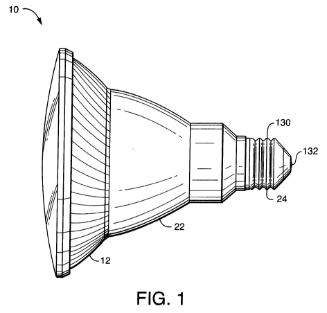
[00016] FIG. 1 shows a side perspective view of a preferred embodiment of an
HID reflector lamp 10. The HID reflector lamp assembly 10 is made from a
reflector 12, a lamp capsule 14, an inner element such as an inner cover 16, a
circuit board 18, a heat sink 20, an outer cover 22 and a thread base 24. A
front
cover lens may also be used to close the forward end of reflector 12.
[00017] FIG. 2 shows a side perspective view of a preferred embodiment of an
integral HID lamp capsule 14, support ring 74 and contact clip 52 assembly.
The HID lamp capsule 14 has a wall 26 defining an enclosed volume 28, and a
sealed end 30 with at least two extending electrical connections, first lead
32,
and second lead 34. The preferred capsule 14 is a tubular lamp capsule with a
press sealed end 30. The preferred lamp capsule 14 includes a ceramic lamp 36,
such as a Power Ball, but any similarly small ceramic or quartz HID lamp
structure may be adapted for use in the present HID lamp capsule 14 structure.
In the preferred embodiment, the ceramic lamp 36 extends axially 37 with a
first end 38 electrically coupled near the sealed end 30 to the first lead 32,
and a
second end 40 coupled through a lead 42 that extends back along but offset
from the long side of the ceramic lamp 36 to be electrically coupled to the
-3-
CA 02723542 2010-11-04
WO 2009/137198 PCT/US2009/039333
second lead 34. This second coupling path 40, 42, 34 is axially longer than
the
other path (38, 32) and provides a better path of the two paths for
suppressing
EMI.
[00018] FIG. 11 shows a perspective view of a preferred embodiment of an
electrically conductive spring clip 52. In the preferred embodiment,
electrically
coupled the second lead 34 is an electrical tap that contacts a metal layer 44
formed on the reflector 12. The preferred tap is a spring steel clip 52 that
clips
with spring arms 54, 56 to the press sealed end 30 of lamp capsule 14. The
clip
52 includes a hole 58 formed with a tab 60 to slide over and then latch with
the
second lead 34, as the rest of the clip 52 mates (clips) with the press sealed
end
30 of the lamp capsule 14. The tab 60 extends from the clip 52 as a spring arm
to make an electrical connection from the second lead 34 to the metal layer 44
formed on the reflector 12.
[00019] FIG. 3 shows a front view of a preferred embodiment of an integral HID
lamp reflector 12. FIG. 4 shows a cross sectional view of a preferred
embodiment of the same preferred reflector 12. FIG. 5 shows a cross sectional
view of a preferred embodiment of the same preferred reflector 12, rotated
axially 90 degrees. The reflector 12 has the form of concave shell with a
front
side 62 and a rear side 64. A neck 66 extends rearward along the reflector's
axis
37 and defines a through passage 68 extending from the front side 62 to the
rear
side 64. The preferred rear side 64 of the neck 66 is formed with one or more
alignment faces, such as the side sloping planar faces 70 to mate with
corresponding faces formed on the inside of the inner element such as inner
cover 16. The reflector 12 has a reflective metal layer 44 on the front side
62.
In the preferred embodiment the reflective metal layer 44 is made with a metal
such as aluminum that extends into the through passage 68 where an electrical
contact to the metal layer 44 may be made, for example with clip 52 with a
spring arm, tab 60. The preferred embodiment, the metal layer 44 extends
substantially around, or as far as practicable, around the body of the lamp
-4-
CA 02723542 2010-11-04
WO 2009/137198 PCT/US2009/039333
capsule 14, such as into the neck 66 and passage 68 region and to the exterior
rim at the front end of the reflector 12. The metal layer 44 then defines an
EMI
capture cage extending substantially around the ceramic lamp 36. It is useful
for electrical connection that the metal layer 44 be sufficiently thick in the
neck
66 and passage 68 area of the reflector 12 to enable sufficient electrical
contact
in the neck 66 region. If the metal layer 44 in the neck 66 is thin, it may be
scratched thorough or may otherwise not provide a sufficiently conductive
connection. Applicants have found it useful to place a small section of
electrically conductive tape (not shown) on the interior of the neck 66 where
the
electrical contact to the metal layer 44 is made. The tape avoids problems
with
making a sufficiently conductive and durable electrical connection to the
coating 44 in the passage 68. It is expected that additional aluminization of
the
neck 66 interior (passage 68) will make the tape unnecessary. The HID lamp
capsule 14 is positioned with its light generating region facing or exposed to
the
reflective metal layer 44, and is otherwise positioned axially 37 to be
aligned in
the reflector neck 66. In the preferred embodiment the front side 62 of the
reflector 12 is also formed with a step and or protruding nubs 72 formed
around
the opening of the through passage 68 to position a spacer ring 74 to brace
between the exterior wall of the lamp capsule 14 and the front side 62 of the
reflector 12. The spacer ring 74 axially positions and braces the lamp capsule
14 in the reflector 12. The electrical connections 32, 34 of the lamp capsule
14
are positioned to be exposed for electrical connection at an end of the neck
66
adjacent the rear side 64 of the reflector 12.
[00020] FIG. 12 shows a rear view of a preferred embodiment of an integral HID
lamp reflector 12. The rear side 64 of the preferred reflector 12 is formed to
include two or more snap recesses 76 and two or more alignment nubs 77 and a
positioning ledge 84. The snap recess 76 may be formed with an indentation 78
to receive and hold a latching face 90 of a corresponding latch 82 formed on
the
inner cover 16. The preferred indentations 78 extend inwards, towards the
-5-
CA 02723542 2010-11-04
WO 2009/137198 PCT/US2009/039333
central axis 37 of the reflector 12. The exterior faces aside the snap recess
76
which may be planer sections adjacent the indentations 78 then face away from
the reflector axis 37 and are preferably parallel with the axis 37. The
preferred
reflector 12 includes circular rib or ledge 84 formed the rear side 64,
extending
around the axis 37 radially exterior from the snap recess 72 that a front rim
86
of the outer cover 22 can be seated on or braced against. The preferred
reflector
12 also includes nub 88 formed along the rib or ledge 84 to key with notch 140
formed on the outer cover 22.
[00021] FIG. 6 shows a front perspective view of a preferred embodiment of an
element in the preferred form of an inner cover 16. FIG. 7 shows a rear
perspective view of the same preferred embodiment of the inner cover 16 of
FIG. 6. The preferred inner element such as inner cover 16 may be made of a
molded plastic resin and has the form of a concave shell that couples to the
reflector 12 to cover a rear portion of the reflector 12. The preferred inner
cover
16 is formed with at least one latch 82 with a latch face 90. The inner cover
16
is similarly formed with two or more alignment guides, such as slots 96 that
are
sized and spaced to mate with the alignment nubs 77 formed on the rear side 64
of the reflector 12. The inner cover 16 also includes an alignment face 98
that
is sized and space so as to fit tightly adjacent the alignment face 70 of the
neck
66. The preferred inner cover 16 is snap fitted to the recesses 76 and
antirotational keyed to the nubs 77 by the slots 96.
[00022] The inner cover 16 is formed with at least one through passage 100
allowing the electrical leads 32, 34 of the lamp capsule 14 to be exposed
along
the rear side 102 of the inner cover 16 for electrical connection. It is
convenient
that the electrical leads 32, 34 extend through and beyond the thickness of
the
inner cover 16. The inner cover 16 may then be fitted to the rear side 64 of
the
reflector 12 butting against the alignment face(s) 70, the nubs 77 and snap
fitting in recess 76. The preferred inner cover 16 is also formed with at
least
two stand up braces 104, block shaped projections, on the rear face 102
adjacent
-6-
CA 02723542 2010-11-04
WO 2009/137198 PCT/US2009/039333
the through passages 100, having faces 106. The rear side of the inner cover
16
is formed with one or more latches, such as spring tab latches 108, that can
couple with corresponding latch faces 136 formed on the inner wall of the
outer
cover 22. In the preferred embodiment the inner cover 16 is formed with four
spring tab latches 108 positioned at 90 degrees around the forward rim of the
inner cover 16.
[00023] In the preferred embodiment, one or more electrical clip 110 extend
through the inner cover 16 with a first face 112 adjacent a respective one of
the
electrical leads 32, 34 and a spring tensioned second face 114 to be exposed
adjacent a respective one of the coupling pads 122 of the circuit board 18 and
formed with a spring tension to form a clamping trap with the face 106. In the
preferred embodiment, for each electrical lead 32, 34 there is a corresponding
electrical clip 110. Each clip 110 is coupled to the inner cover 16 in the
neck
region of the inner cover with a first face 112 adjacent a respective one the
electrical leads 32, 34 and a second face 114 exposed along a linear slot
region
116 and positioned to be opposite the front faces 106 of the braces 104. The
preferred second faces 114 of the clips 110 are formed to have a spring
tension
in the direction of the braces 104. The respective electrical clips 110 are
electrically coupled along the first faces 112 to the corresponding electrical
leads 32, 34 for example by welding, soldering or crimping the respective
electrical leads 32, 34 to the clip 110 respective along the first faces 112.
The
electrical clip 110 is electrically coupled to a corresponding one of the
electrical
leads 32, 34, and forms a socket like coupling for the circuit board 18. In
the
preferred embodiment, the electrical contact faces 114 are aligned to face in
opposite directions, and are separated and offset from the linear slot 116
defining a channel along which the edge of the circuit board 18 butts into.
[00024] FIG. 8 shows a rear perspective view of a preferred embodiment of an
inner cover 16 coupled to a preferred embodiment of a circuit board 18. A
planar circuit board 18 having control circuitry 118 for controlling
electrical
-7-
CA 02723542 2010-11-04
WO 2009/137198 PCT/US2009/039333
power supplied to the HID lamp capsule 36 is positioned so the circuit board
18
has an edge 120 mechanically coupled to the inner cover 16 and positioned to
electrically contact the electrical coupling face 114 supported on the inner
cover
16. In the preferred embodiment, the circuit board 18 is formed as a planar
body having a thickness corresponding to the distance between the stand up
brace face 106 and the spring tensioned second face 114 of the clip 110, so
the
edge 120 of the circuit board 18 may be securely slotted into and pinched
between the clips 110 and the braces 104.
[00025] The circuit board 18 is formed with control circuitry 118 for
controlling
electrical power supplied to the HID lamp capsule 14. Various control circuits
are known in the art, and any convenient one may be used according to the
user's preference. The circuit board 18 is formed with respective electrical
contacts, such as metal pads 122 or trace lines, formed on the circuit board
18 to
contact the respective second faces 114 of the clips 110. The preferred
contacts
122 are formed on opposite sides of the circuit board 18. Because the lamp
capsule 14 is operated by a high voltage power supply, it is preferred to
offset
the lead inputs and outputs by insulation and distance. In the preferred
embodiment, the electrical contacts are formed as metal pads 122 on opposite
sides of the circuit board 18 and separated linearly along the edge 120 of the
circuit board 18. This high resistance material forms a high resistance path
between the lead couplings, thereby providing for high creep and contact
clearance. This enables closer positioning of the circuit board. The
electrical
circuit board 18 is otherwise preferably extended rearward with the plane of
the
circuit board 18 extending parallel to the lamp axis 37 away from the lamp
capsule 14 and the inner cover 16. The preferred circuit board 18 is otherwise
formed with all circuit 118 components spaced so as to leave an open track 124
around the edge region and if necessary across the center region of the
circuit
board 118 that is wide enough so that an edge wall 126 of the heat sink 20 can
pinch to the circuit board 18 without interfering with the circuit board 18
-8-
CA 02723542 2010-11-04
WO 2009/137198 PCT/US2009/039333
operations. The heat sink 20 while acting as a heat sink, then also encloses
the
relevant circuit board 18 components to provide a floating or pseudo ground
EMI shield with respect to the circuit board 18.
[00026] FIG. 9 shows a cross sectional view of a preferred embodiment of an
inner
cover 16 coupled to a preferred embodiment of a circuit board 18 enclosed in
part by a preferred embodiment of a heat sink and EMI shield 20. In the
preferred embodiment, the circuit board 18 is surrounded by an electrically
conductive heat sink 20. The preferred heat sink 20 has the form of a concave
shell formed to span at least one side of the circuit board 18. In the
preferred
embodiment, the heat sink 20 is formed in two halves that bracket the circuit
board 18. Preferably both sides of the circuit board 18 are then enclosed in
the
two half shells forming the heat sink 20 structure. The heat sink 20 has in
internal side 128 with that preferably includes mechanical contacts 130
positioned adjacent the circuit board 18 or components formed thereon, for
contact with the circuit board 18 or the components to conduct heat away from
the circuit board 18 or components. The preferred heat sink 20 has an external
side 132 formed with heat dispersing features, such as fins 134 and otherwise
defines an electrically conductive, and substantially complete enclosure
around
at least any significant EMI emitting components carried on the circuit board
18. A significant EMI emitting component is one that emits sufficient EMI to
make the final product unacceptable to a user, such are interference with a
near
by radio or TV receiver, telephone, CRT computer or similar device. The
circuit board 18 is then enclosed by a heat sink 20 assembly forming a
substantially closed electromagnetic interference (EMI) blocking housing. The
combined heat sink and EMI shield 20 then provides a floating or pseudo
ground with respect to the circuit board 118. It is understood that there may
be
some electrical connections or circuit board components that are insignificant
EMI emitters that extend beyond the enclosed volume of the heat sink 20
structure, and that there may not be an exact hermetic seal between the
circuit
-9-
CA 02723542 2010-11-04
WO 2009/137198 PCT/US2009/039333
board 18 and the heat sink 20 structure, but that such openings may be
constrained to be narrow, thereby providing minimal opportunity for EMI
leakage out of the enclosed cavity 138. The preferred heat sink 20 includes
along its exterior surface 132 one or more axially extending keying features
such as axially extending slots to align and key with the outer cover 22. The
Applicants have found it convenient to pinch the two half shells forming the
heat sink 20 with tight contact from the adjacent inner wall of the outer
cover
22.
[00027] FIG. 10 shows a cross sectional view of a preferred embodiment of an
outer cover 22. The outer cover 22 encloses the inner cover 16, circuit board
18, and the heat sink 20 assembly. The outer cover 22 is coupled to or closed
by the base 24 that has external electrical connections 130, 132 for coupling
in
an electrical socket (not shown), such as a typical threaded lamp socket to
the
internal electrical connections 32, 34 through the circuit board 18. The base
24
may be crimped, threaded, riveted, glued or otherwise attached to an end of
the
outer cover 22.
[00028] The outer cover 22 is shaped to enclose the inner cover 16, the
circuit
board 18, and heat sink 20. The outer cover 22 has internal contacts,
couplings
or wall portions such as an upstanding tab 134 positioned to be closely
adjacent
the exterior side of inner cover snaps 82. In this way, the tabs 134 of outer
cover 22 pins the snaps 82 of the inner cover 16 in place against the snap
recess
76 formed on the reflector 12. The snaps 82 along their respective rear sides
(radially exterior sides) are then blocked by the inside wall of the outer
cover,
such as by the tabs 134 of the outer cover 22 and as a result are fixed in
place
against the snap recesses 76 and cannot be withdrawn until the outer cover 22
is
moved to unblock the constrained snaps 82. The outer cover 22 also includes
one or more internal or hidden latches 136 that couple to the corresponding
latch(es) 108 on the inner cover 16. In the preferred embodiment, the outer
cover 22 has four internal latches 136 positioned at 90 degrees around the
axis
-10-
CA 02723542 2010-11-04
WO 2009/137198 PCT/US2009/039333
to close respectively with the four latches 108 on the inner cover 16. The
inner
cover 16 is then covered by and blindly latched to the outer cover 22. Since
the
inner cover 16 and outer cover 22 are blindly latched the inner cover 16 and
outer cover 22 cannot be separated once they are snapped together. In the
preferred embodiment the outer cover also includes one or more guides 138,
such as axially extending ribs that key with corresponding keys, such as
axially
extending slots (not shown) formed on the exterior surface 132 of the heat
sink
20. As the outer cover 22 is positioned over the inner cover 16, the guides
138
slidingly key with the matching keys, such as slots, of the heat sink 20,
aligning
the inner assembly and the outer cover 22. The outer cover 22 also includes a
key, such as a notch 140 formed to mate with a corresponding key feature, such
as an upstanding nub 88 formed on the reflector 12. The reflector 12 and the
outer cover 22 are then keyed one to the other, and cannot be axially rotated
separately when properly positioned. In the preferred embodiment, the outer
cover 22 is further braced along its forward rim 86 against the reflector
ledge 84
to be further stabilized with respect the reflector 12. Alternatively the
outer
cover 22 could be coupled along the forward rim 85 of the reflector 12. The
outer cover 22 need not be glued to the reflector 12. It is understood that a
glue
or water sealant could be applied along the exterior facing seams of the
assembly for water sealing, but it is not necessary for mechanical coupling of
the assembly. The outer cover 22 is then aligned by and axially snap fitted to
latch elements formed on the assembly of the reflector 12, the inner cover 16
and the heat sink 20 structures. The outer cover 22 may further include one or
more internally formed guides, such as slots or notches that exposed edge
portions of the circuit board 18 can be inserted in or aligned with. Once in
position, the outer cover 22 is then permanently aligned by and clipped to the
reflector, inner cover, circuit board and heat sink assembly. It cannot be
unclipped from, or rotated with respect to the reflector, inner cover, circuit
board and heat sink assembly.
-11-
CA 02723542 2010-11-04
WO 2009/137198 PCT/US2009/039333
[00029] The base 24 may be coupled to the outer cover 22 and formed with
external electrical connections 130, 132 for coupling in a lamp socket, such
as a
threaded socket. One of the typical threaded base couplings may be used. The
base 24 otherwise provides internal electrical connections to the circuit
board
18.
[00030] The lamp may be assembled by loosely clamping the heat sink and EMI
shield to the circuit board. The circuit board and heat shield assembly is
then
inserted in the outer cover, aligning the guide features (slots) of the heat
shield
with the corresponding features (tabs) formed on the interior of outer cover.
The heat sink EMI shield is then pinned or pinched in close contact with the
circuit board by wedging pressure from the outer cover. The inner cover is
aligned by the alignment faces and nubs formed on the rear of the reflector
and
clipped to the latch features formed on the rear of the reflector. The lamp
capsule, alignment ring and grounding clip assembly are then inserted into the
front side of the reflector with the capsule leads threaded through the
openings
in the inner cover adjacent the weld points. Simultaneously the EMI contact
arm is forced into conductive contact with the metallized surface of the
reflector, and the positioning ring is settled with its alignments along the
front
side of the reflector. The lamp leads are then welded (soldered, or crimped)
to
the contact points on the clips supported on the inner cover. The outer cover
assembly is then aligned with and pressed onto the reflector assembly. The
circuit board is then captured in the alignment channel (slot), and
electrically
coupled to the lamp leads through the clips grasping or clamping the edge of
the
circuit board. The outer cover then latches to the inner cover, while
simultaneously positioning closely behind the inner cover latches, blocking
the
withdrawal of the latches form the reflector. The outer cover assembly is
thereby permanently latched to the reflector assembly. Leads from the circuit
board are then coupled to the threaded base, and the threaded base is fixed to
the cover, for example by crimping an edge of the threaded base to the outer
-12-
CA 02723542 2010-11-04
WO 2009/137198 PCT/US2009/039333
cover. A cover lens may then be fitted to the front of the reflector and fixed
in
place for example by silicone cement, epoxy or flame sealing.
[00031] While there have been shown and described what are at present
considered
to be the preferred embodiments of the invention, it will be apparent to those
skilled in the art that various changes and modifications can be made herein
without departing from the scope of the invention defined by the appended
claims.
-13-