Note: Descriptions are shown in the official language in which they were submitted.
CA 02723599 2010-11-04
WO 2009/137722 PCT/US2009/043208
CARBON NANOTUBE-BASED COAXIAL ELECTRICAL
CABLES AND WIRING HARNESS
TECHNICAL FIELD
[0001] The present invention relates to the formation of a cable, and more
particularly, to a conducting member made from a nanostructure-based material
and a shielding layer made from a material capable of providing substantially
low resistance coupling.
BACKGROUND ART
[0002] Carbon nanotubes are known to have extraordinary tensile strength,
including high strain to failure and relatively high tensile modulus. Carbon
nanotubes may also be highly resistant to fatigue, radiation damage, and heat.
To this end, the addition of carbon nanotubes to composite materials can
increase tensile strength and stiffness of the composite materials.
[0003] Within the last fifteen (15) years, as the properties of carbon
nanotubes
have been better understood, interests in carbon nanotubes have greatly
increased within and outside of the research community. One key to making
use of these properties is the synthesis of nanotubes in sufficient quantities
for
them to be broadly deployed. For example, large quantities of carbon nanotubes
may be needed if they are to be used as high strength components of composites
in macroscale structures (i.e., structures having dimensions greater than 1
cm.)
[0004] One common route to nanotube synthesis can be through the use of gas
phase pyrolysis, such as that employed in connection with chemical vapor
deposition. In this process, a nanotube may be formed from the surface of a
catalytic nanoparticle. Specifically, the catalytic nanoparticle may be
exposed
to a gas mixture containing carbon compounds serving as feedstock for the
generation of a nanotube from the surface of the nanoparticle.
[0005] Recently, one promising route to high-volume nanotube production has
been to employ a chemical vapor deposition system that grows nanotubes from
1
CA 02723599 2010-11-04
WO 2009/137722 PCT/US2009/043208
catalyst particles that "float" in the reaction gas. Such a system typically
runs a
mixture of reaction gases through a heated chamber within which the nanotubes
may be generated from nanoparticles that have precipitated from the reaction
gas. Numerous other variations may be possible, including ones where the
catalyst particles may be pre-supplied.
[0006] In cases where large volumes of carbon nanotubes may be generated,
however, the nanotubes may attach to the walls of a reaction chamber,
resulting
in the blockage of nanomaterials from exiting the chamber. Furthermore, these
blockages may induce a pressure buildup in the reaction chamber, which can
result in the modification of the overall reaction kinetics. A modification of
the
kinetics can lead to a reduction in the uniformity of the material produced.
[0007] An additional concern with nanomaterials may be that they need to be
handled and processed without generating large quantities of airborne
particulates, since the hazards associated with nanoscale materials are not
yet
well understood.
[0008] The processing of nanotubes or nanoscale materials for macroscale
applications has steadily increased in recent years. The use of nanoscale
materials in textile fibers and related materials has also been increasing. In
the
textile art, fibers that are of fixed length and that have been processed in a
large
mass may be referred to as staple fibers. Technology for handling staple
fibers,
such as flax, wool, and cotton has long been established. To make use of
staple
fibers in fabrics or other structural elements, the staple fibers may first be
formed into bulk structures such as yarns, tows, or sheets, which then can be
processed into the appropriate materials.
[0009] Accordingly, it would be desirable to provide a material that can take
advantage of the characteristics and properties of carbon nanotubes, so that a
cable made of carbon nanotubes can be processed for end use applications.
SUMMARY OF THE INVENTION
2
CA 02723599 2010-11-04
WO 2009/137722 PCT/US2009/043208
[00010] The present invention provides, in accordance with one embodiment, a
cable. In an embodiment, the cable may include a conducting member made
from a nanostructure-based material, a shielding layer made of nanostructure-
based material and circumferentially situated about the conducting member so
as to enhance conductivity along the conducting member, and a coupling
mechanism situated between the shielding layer and the conducting member so
as to secure the shielding layer in its position on the conducting member.
[00011] The present invention provides, in accordance with another embodiment,
a method for making a cable. The method may include providing a conducting
member made from a nanostructure-based material, placing a shielding layer
circumferentially about the conducting member, and applying a coupling
mechanism between the shielding layer and the conducting member so as to
secure the shielding layer in its position about the conducting member.
BRIEF DESCRIPTION OF DRAWINGS
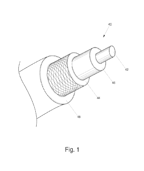
[00012] Figs. 1 illustrates a cable in accordance with one embodiment of the
present invention.
[00013] Fig. 2 illustrates the break even frequencies for conducting members
made in accordance with one embodiment of the present invention.
[00014] Fig. 3 illustrates the break even frequencies for conducting members
made in accordance with another embodiment of the present invention.
[00015] Fig. 4 illustrates electrical properties of carbon nanotubes made in
accordance with one embodiment of the present invention.
[00016] Fig. 5 illustrates resistivity versus temperature characteristics of
carbon
nanotubes made in accordance with one embodiment of the present invention.
[00017] Fig. 6 illustrates resistivity versus temperature characteristics of
carbon
nanotubes in (and out of) the presence of a magnetic field.
[00018] Fig. 7 illustrates a system for formation and harvesting of
nanofibrous
materials in accordance with one embodiment of the present invention.
3
CA 02723599 2010-11-04
WO 2009/137722 PCT/US2009/043208
[00019] Fig. 8 illustrates a Chemical Vapor Deposition system for fabricating
nanotubes, in accordance with one embodiment of the present invention.
[00020] Fig. 9 illustrates another variation of the system of the present
invention
for formation and harvesting of nanofibrous materials.
[00021] Fig. 10 illustrates a system of the present invention for formation
and
harvesting of nanofibrous materials.
[00022] Fig. 11 illustrates a cable in accordance with another embodiment of
the
present invention.
[00023] Fig. 12 illustrates resistance properties for a cable of the present
invention is compared to those properties exhibited by copper wires or Litz
wires.
[00024] Fig. 13 illustrates the relationship between frequency of a cable of
the
present invention and thickness of the cable.
[00025] Fig. 14 illustrates resistance versus current properties for a cable
made in
accordance with an embodiment of the present invention as compared to those
properties exhibited by copper wires or Litz wires
[00026] Fig. 15 illustrates current versus temperature properties for a cable
of the
present invention.
[00027] Fig. 16 illustrates another embodiment of the present invention in
which
the cable is part of a wiring harness.
DESCRIPTION OF SPECIFIC EMBODIMENTS
[00028] The present invention provides, in accordance with one embodiment, a
cable. In an embodiment, the cable, as shown in Fig. 1, may include a
conducting member 42 made from a nanostructure-based material. The cable
may also include a shielding layer positioned about the conducting member 42.
The cable may further include an insulation layer to improve conductivity and
reduce resistivity of the cable. The cable may further include a coupling
mechanism situated between the conducting member 42 and the shielding layer.
4
CA 02723599 2010-11-04
WO 2009/137722 PCT/US2009/043208
The coupling mechanism may act to secure the shielding layer on the cable.
The coupling mechanism further acts to maintain transmission of current along
the conducting member 42.
[00029] Presently, there exist multiple processes and variations thereof for
growing nanotubes, and forming sheets or cable structures made from these
nanotubes. These include: (1) Chemical Vapor Deposition (CVD), a common
process that can occur at near ambient or at high pressures, and at
temperatures
above about 400 C, (2) Arc Discharge, a high temperature process that can
give
rise to tubes having a high degree of perfection, and (3) Laser ablation.
[00030] The present invention, in one embodiment, employs a CVD process or
similar gas phase pyrolysis procedures known in the industry to generate the
appropriate nanostructures, including carbon nanotubes. Growth temperatures
for a CVD process can be comparatively low ranging, for instance, from about
400 C to about 1350 C. Carbon nanotubes, both single wall (SWNT) or
multiwall (MWNT), may be grown, in an embodiment of the present invention,
by exposing nanoscaled catalyst particles in the presence of reagent carbon-
containing gases (i.e., gaseous carbon source). In particular, the nanoscaled
catalyst particles may be introduced into the reagent carbon-containing gases,
either by addition of existing particles or by in situ synthesis of the
particles
from a metal-organic precursor, or even non-metallic catalysts. Although both
SWNT and MWNT may be grown, in certain instances, SWNT may be selected
due to their relatively higher growth rate and tendency to form rope-like
structures, which may offer advantages in handling, thermal conductivity,
electronic properties, and strength.
[00031] The strength of the individual carbon nanotubes generated in
connection
with the present invention may be about 30 GPa or more. Strength, as should
be noted, is sensitive to defects. However, the elastic modulus of the carbon
nanotubes fabricated in the present invention may not be sensitive to defects
and
can vary from about 1 to about 1.2 TPa. Moreover, the strain to failure of
these
nanotubes, which generally can be a structure sensitive parameter, may range
from a about 10% to a maximum of about 25% in the present invention.
CA 02723599 2010-11-04
WO 2009/137722 PCT/US2009/043208
[00032] Furthermore, the nanotubes of the present invention can be provided
with relatively small diameter. In an embodiment of the present invention, the
nanotubes fabricated in the present invention can be provided with a diameter
in
a range of from less than 1 nm to about 10 nm.
[00033] The nanotubes of the present invention can also be used as a
conducting
member to carry relatively high current similar to a Litz wire or cable.
However, unlike a Litz wire or cable soldered to a connector portion, the
nanotube conducting member of the present invention can exhibit relatively
lower impedance in comparison. In particular, it has been observed in the
present invention that the shorter the current pulses, the better the nanotube-
based wire cable or ribbon would perform when compared with a copper ribbon
or Litz wire. One reason for the observed better performance may be that the
effective frequency content of the pulse, which can be calculated from the
Fourier Transform of the waveform for current pulses that are square and
short,
e.g., about 100 ms to less than about 1 ms, can be very high. Specifically,
individual carbon nanotubes of the present invention can serve as conducting
pathways, and due to their small size, when bulk structures are made from
these
nanotubes, the bulk structures can contain extraordinarily large number of
conducting elements, for instance, on the order of 1014/cm2 or greater.
[00034] Carbon nanotubes of the present invention can also demonstrate
ballistic
conduction as a fundamental means of conductivity. Thus, materials made from
nanotubes of the present invention can represent a significant advance over
copper and other metallic conducting members under AC current conditions.
However, joining this type of conducting member to an external circuit
requires
that essentially each nanotube be electrically or thermally contacted to avoid
contact resistance at the junction.
[00035] Carbon nanotubes of the present invention can exhibit certain
characteristics which are shown in Figs. 2-6. Fig. 2 shows the break even
frequencies for conductors made of a carbon nanotube wire, a copper wire, and
a Litz wire. Resistance is influenced by several factors, including skin
effect,
proximity effect, and conductor shape. Moreover, resistance is also influenced
6
CA 02723599 2010-11-04
WO 2009/137722 PCT/US2009/043208
by DC behavior where copper is approximately sixty times stronger. Fig. 3
shows the same calculations as Fig. 2 using much thicker carbon nanotube
wires. The break even frequencies for the thicker carbon nanotube wires are
lower. Fig. 4 illustrates the electrical properties of carbon nanotubes made
in
accordance with one embodiment of the present invention. Fig. 5 illustrates
the
resistivity of these carbon nanotubes in relation to temperature. Fig. 6
illustrates
characteristics of carbon nanotube resistivity versus temperature in (and out
of)
the presence of a magnetic field.
[00036] It should be noted that although reference is made throughout the
application to nanotubes synthesized from carbon, other compound(s), such as
boron, MoS2, or a combination thereof may be used in the synthesis of
nanotubes in connection with the present invention. For instance, it should be
understood that boron nanotubes may also be grown, but with different
chemical precursors. In addition, it should be noted that boron may also be
used
to reduce resistivity in individual carbon nanotubes. Furthermore, other
methods, such as plasma CVD or the like can also be used to fabricate the
nanotubes of the present invention.
Cable Formation
[00037] To carry relatively high current pulses between two conductors, such
as
a high energy capacitor, a ground strap, a bus bar or bus pipe, or pulse
generating circuit, to an external circuit without degradation of the waveform
or
without heating of a junction, the present invention provides, in an
embodiment,
a conductive cable, such as that shown in Fig. 1. The conductive cable may be,
in an embodiment, a coaxial cable 40. The coaxial cable 40 may include,
among other things, a conducting member 42 made from a nanostructure-based
material and a shielding layer 44 circumferentially situated about the
conducting
member 42 and made from a material capable of providing substantially low
resistance coupling, such as, sheet 26. It should be noted that this coaxial
cable
40 arrangement is being provided only for illustrative purposes and other
configurations may be possible.
7
CA 02723599 2010-11-04
WO 2009/137722 PCT/US2009/043208
[00038] In accordance with one embodiment, the coaxial cable 40 may include a
conducting member 42 made from a nanostructure-based material. The
nanostructure-based material, in an embodiment, may be defined by yarns,
ribbons, wires, cables, tapes or sheets made in accordance with the present
invention from carbon nanotubes fabricated in a manner similar to that
disclosed in U.S. Patent Application No. 11/488,387 to Lashmore et al. (which
application is hereby incorporated in its entirety by reference). For tapes
and
sheets, they may be rolled into a cylindrical shape to form the conducting
member 42.
Formation of Conducting Member
[00039] With reference now to Fig. 7, under steady-state production using a
CVD process of the present invention, nanotubes 51 may be collected from
within a synthesis chamber 52 and a yarn 53 may thereafter be formed.
Specifically, as the nanotubes 51 emerge from the synthesis chamber 52, they
may be collected into a bundle 54, fed into intake end 55 of a spindle 56, and
subsequently spun or twisted into yarn 53 therewithin. It should be noted that
a
continual twist to the yarn 53 can build up sufficient angular stress to cause
rotation near a point where new nanotubes 51 arrive at the spindle 56 to
further
the yarn formation process. Moreover, a continual tension may be applied to
the yarn 53 or its advancement into collection chamber 58 may be permitted at
a
controlled rate, so as to allow its uptake circumferentially about a spool 57.
[00040] Typically, the formation of the yarn results from a bundling of
nanotubes that may subsequently be tightly spun into a twisting yarn.
Alternatively, a main twist of the yarn may be anchored at some point within
system 10 and the collected nanotubes may be wound on to the twisting yarn.
Both of these growth modes can be implemented in connection with the present
invention.
[00041] The conducting member 42 may be made from one of carbon, copper,
silver, boron-nitride, boron, MoS2, or a combination thereof. Moreover, the
material from which the conducting member 42 may be made can include, in an
embodiment, graphite of any type, for example, such as that from pyrograph
8
CA 02723599 2010-11-04
WO 2009/137722 PCT/US2009/043208
fibers. The conducting member 42 may be designed to transmit electrical
signals such as AC, DC, low power, or high power. In an embodiment, the
conducting member 42 may range from about 1 to about 3 percent by weight of
the entire structure. Of course, this range is only for illustrative purposes,
and a
smaller or larger range can be employed.
Fabricatin Sheets
[00042] With reference now to Fig. 9, there is illustrated a system 10,
similar to
that disclosed in U.S. Patent Application Serial No. 11/488,387 (incorporated
herein by reference), for use in the fabrication of nanotubes. System 10, in
an
embodiment, may be coupled to a synthesis chamber 11. The synthesis
chamber 11, in general, includes an entrance end 111, into which reaction
gases
(i.e., gaseous carbon source) may be supplied, a hot zone 112, where synthesis
of extended length nanotubes 113 may occur, and an exit end 114 from which
the products of the reaction, namely the nanotubes and exhaust gases, may exit
and be collected. The synthesis chamber 11, in an embodiment, may include a
quartz tube 115 extending through a furnace 116. The nanotubes generated by
system 10, on the other hand, may be individual single-walled nanotubes,
bundles of such nanotubes, and/or intertwined single-walled nanotubes (e.g.,
ropes of nanotubes).
[00043] System 10, in one embodiment of the present invention, may also
include a housing 12 designed to be substantially airtight, so as to minimize
the
release of potentially hazardous airborne particulates from within the
synthesis
chamber 11 into the environment. The housing 12 may also act to prevent
oxygen from entering into the system 10 and reaching the synthesis chamber 11.
In particular, the presence of oxygen within the synthesis chamber 11 can
affect
the integrity and compromise the production of the nanotubes 113.
[00044] System 10 may also include a moving belt 120, positioned within
housing 12, designed for collecting synthesized nanotubes 113 made from a
CVD process within synthesis chamber 11 of system 10. In particular, belt 120
may be used to permit nanotubes collected thereon to subsequently form a
substantially continuous extensible structure 121, for instance, a non-woven
or
9
CA 02723599 2010-11-04
WO 2009/137722 PCT/US2009/043208
woven sheet. Such a sheet 26 may be generated from compacted, substantially
non-aligned, and intermingled nanotubes 113, bundles of nanotubes, or
intertwined nanotubes (e.g., ropes of nanotubes), with sufficient structural
integrity to be handled as a sheet 26.
[00045] To collect the fabricated nanotubes 113, belt 120 may be positioned
adjacent the exit end 114 of the synthesis chamber 11 to permit the nanotubes
to
be deposited on to belt 120. In one embodiment, belt 120 may be positioned
substantially parallel to the flow of gas from the exit end 114, as
illustrated in
Fig. 8. Alternatively, belt 120 may be positioned substantially perpendicular
to
the flow of gas from the exit end 114 and may be porous in nature to allow the
flow of gas carrying the nanomaterials to pass therethrough. Belt 120 may be
designed as a continuous loop, similar to a conventional conveyor belt. To
that
end, belt 120, in an embodiment, may be looped about opposing rotating
elements 122 (e.g., rollers) and may be driven by a mechanical device, such as
an electric motor. Alternatively, belt 120 may be a rigid cylinder. In one
embodiment, the motor may be controlled through the use of a control system,
such as a computer or microprocessor, so that tension and velocity can be
optimized.
[00046] Looking at Fig. 9, system 20 may include a pressure applicator, such
as
roller 25, situated adjacent belt 24 to apply a compacting force (i.e.,
pressure)
onto the collected nanomaterials. In particular, as the nanomaterials get
transported toward roller 25, the nanomaterials on belt 24 may be forced to
move under and against roller 25, such that a pressure may be applied to the
intermingled nanomaterials while the nanomaterials get compacted between belt
24 and roller 25 into a coherent substantially-bonded sheet 26. To enhance the
pressure against the nanomaterials on belt 24, a plate 244 may be positioned
behind belt 24 to provide a hard surface against which pressure from roller 25
can be applied. It should be noted that the use of roller 25 may not be
necessary
should the collected nanomaterials be ample in amount and sufficiently
intermingled, such that an adequate number of contact sites exists to provide
the
necessary bonding strength to generate the sheet 26.
CA 02723599 2010-11-04
WO 2009/137722 PCT/US2009/043208
[00047] To disengage the sheet 26 of intermingled nanomaterials from belt 24
for subsequent removal from housing 22, a scalpel or blade 27 may be provided
downstream of the roller 25 with its edge against surface 245 of belt 24. In
this
manner, as sheet 26 moves downstream past roller 25, blade 27 may act to lift
the sheet 26 from surface 245 of belt 24.
[00048] Additionally, a spool or roller 28 may be provided downstream of blade
27, so that the disengaged sheet 26 may subsequently be directed thereonto and
wound about roller 28 for harvesting. As the sheet 26 is wound about roller
28,
a plurality of layers may be formed. Of course, other mechanisms may be used,
so long as the sheet 26 can be collected for removal from the housing 22
thereafter. Roller 28, like belt 24, may be driven, in an embodiment, by a
mechanical drive, such as an electric motor 281, so that its axis of rotation
may
be substantially transverse to the direction of movement of the sheet 26. In
an
alternate embodiment, a blade does not have to be in use to remove the sheet
26.
Rather, removal of the sheet 26 may be by hand or by other known methods in
the art.
[00049] In order to minimize bonding of the sheet 26 to itself as it is being
wound about roller 28, a separation material 29 (see Fig. 10) may be applied
onto one side of the sheet 26 prior to the sheet 26 being wound about roller
28.
The separation material 29 for use in connection with the present invention
may
be one of various commercially available metal sheets or polymers that can be
supplied in a continuous roll 291. To that end, the separation material 29 may
be pulled along with the sheet 26 onto roller 28 as sheet 26 is being wound
about roller 28. It should be noted that the polymer comprising the separation
material 29 may be provided in a sheet, liquid, or any other form, so long as
it
can be applied to one side of sheet 26. Moreover, since the intermingled
nanotubes within the sheet 26 may contain catalytic nanoparticles of a
ferromagnetic material, such as Fe, Co, Ni, etc., the separation material 29,
in
one embodiment, may be a non-magnetic material, e.g., conducting or
otherwise, so as to prevent the sheet 26 from sticking strongly to the
separation
material 29. In an alternate embodiment, a separation material may not be
necessary.
11
CA 02723599 2010-11-04
WO 2009/137722 PCT/US2009/043208
[00050] Once a sheet 26 is generated, the sheet 26 may undergo treatment to
increase conductivity and productivity. Treatment of a sheet 26 after
formation
may, in an embodiment, include subjecting the sheet 26 to a protonation agent.
One feature of the protonation agent may be to bring the carbon nanotubes in
closer proximity with one another. By bringing the carbon nanotubes closer
together, the protonation agent may act to reduce surface tension, reduce
resistivity, and increase conductivity of the sheet 26. Examples of a
protonation
agent may include an acid such as hydronium ion, hydrochloric acid,
hydrobromic acid, hydrofluoric acid, hydroiodic acid, carbonic acid, sulfuric
acid, nitric acid, fluorosulfuric acid, chlorosulfonic acid, methane sulfonic
acid,
trifluoromethane sulfonic acid, oleum, an agent thereof, or a combination
thereof, or other materials capable of being electrically and/or thermally
conductive.
[00051] In an alternate embodiment, treatment of the sheet 26 may further
include spraying the sheet 26 with a solution as it exits the furnace and is
collected on the belt. The solution may contain compounds that cover the outer
surface of the nanotubes in such a manner as to enhance alignment of the
carbon
nanotubes and allow the carbon nanotubes to come into closer proximity with
one another. In an embodiment, the solution may include a solvent, a polymer,
a metal, or a combination thereof. Examples of a solvent that can be used in
connection with the solution include toluene, kerosene, benzene, hexanes,
acetone or any other solvent. Examples of a polymer that can be used in
connection with the solution include polyurethane, polyethylene, poly(styrene
butadiene), polychloroprene, poly(vinyl alcohol), poly(vinyl pyrrolidone),
poly(acrylonitrile-co-butadiene-co-styrene), epoxy, or any polymer. Examples
of a metal that can be used in connection with the solution include a salt,
metal
oxide, or any other metal.
[00052] Once the sheet 26 has been treated, the treated sheet 26 may be
subject to
a heat source for processing of the sheet 26. For example, the sheet 26 may be
subject to sintering, hot isostatic pressing, hot pressing, cold isostatic
pressing
12
CA 02723599 2010-11-04
WO 2009/137722 PCT/US2009/043208
so as to yield a composite sheet or the desired form of the final product.
[00053] Treatment of the composite sheet may, in another embodiment, further
include infusing the composite sheet with a glassy carbon material so as to
increase the structural integrity of the sheet and provide substantially low
resistance coupling. Glassy carbon, in general, may be a form of carbon
related
to carbon nanotubes and can contain a significant amount of graphene like
ribbons comprising a matrix of amorphous carbon. These ribbons include sp2
bonded ribbons that can be substantially similar to the sp2 bonded nanotubes.
As a result, they can have relatively good thermal and electrical
conductivity.
Examples of precursor materials from which glassy carbon can be made include
furfuryl alcohol, RESOL resin (i.e., catalyzed alkyl-phenyl formaldehyde),
PVA, or liquid resin or any material known to form glassy carbon when heat
treated. Of course, other commercially available glassy carbon materials or
precursor materials can be used.
[00054] After the composite sheet is generated, it may be left as a composite
sheet or it may be cut into smaller segments, such as strips. In an
embodiment,
a laser may be used to cut the composite sheet into strips. The laser beam
may,
in an embodiment, be situated adjacent the housing such that the laser may be
directed at the composite sheet as it exits the housing. A computer or program
may be employed to control the operation of the laser beam and also the
cutting
of the strip. In an alternative embodiment, any mechanical means or other
means known in the art may be used to cut the composite sheet 26 into strips.
Formation of Cable
[00055] To form the cable of the present invention, the conducting member 42
may be provided with a shielding layer 44. In shielding layer 44, in an
embodiment, may be made from a nanostructure-based material. The
nanostructure-based material, in one embodiment, can be those made from
conductive carbon nanotube, for instance, yarns, tapes, cables, ribbons, or
sheets
made from carbon nanotubes. The shielding layer, on the other hand, may be
made from sheets made from carbon nanotubes so long as the material can be
electrically and/or thermally conductive. In an embodiment, the shielding
layer
13
CA 02723599 2010-11-04
WO 2009/137722 PCT/US2009/043208
44 may range from about 4 to about 7 percent by weight of the entire
structure.
Of course, this range is only for illustrative purposes, and a smaller or
larger
range can be employed. The shielding layer 44, in an embodiment, when
coupled to conducting member 42, can permit high current from a source to be
directed along the conducting member 42 to an external circuit without
substantial degradation. This is because nanotubes defining the shielding
layer
44 of the present invention can act to minimize RF signals or other
electromagnetic waves or signals from being leaked to or from the conducting
member 42. Of course, any other material available commercially that can act
to minimize RF signals or other electromagnetic waves or signals from being
leaked to or from the conducting member 42 may be used in place of shielding
layer 44.
[00056] To the extent desired, the coaxial cable 40 can also include
insulation to
improve conductivity and reduce resistivity of the coaxial cable 40. In an
embodiment, the coaxial cable 40 may include at least one insulation layer 46
circumferentially situated between the conducting member 42 and shielding
layer 44. Insulation layer 46 may be made from a strip of carbon nanotubes,
which had been cut from a sheet 26, and may range from about 33 to about 37
percent by weight of the entire structure. In one embodiment, the coaxial
cable
40 may further include a second insulation layer 48 circumferentially situated
about the shielding layer 44. The second insulation layer 48 may be made from
a strip of carbon nanotubes, which had been cut from a sheet 26, and may range
from about 55 to about 60 percent by weight of the entire structure. Of
course,
these ranges are only for illustrative purposes, and a smaller or larger range
can
be employed. In addition, any other insulative material available commercially
may be used in place of insulation layers 46, 48.
[00057] The coaxial cable 40 may further include a coupling mechanism situated
between the conducting member 42 and the shielding layer 44, so as to secure
the shielding layer 44 in its position about the conducting member 42. In one
embodiment, the coupling mechanism may be made from a glassy carbon
material capable of providing substantially low resistance coupling. Glassy
carbon, in general, may be a form of carbon related to carbon nanotubes and
can
14
CA 02723599 2010-11-04
WO 2009/137722 PCT/US2009/043208
contain a significant amount of graphene like ribbons comprising a matrix of
amorphous carbon. These ribbons include sp2 bonded ribbons that can be
substantially similar to the sp2 bonded nanotubes. As a result, they can have
relatively good thermal and electrical conductivity. Examples of precursor
materials from which glassy carbon can be made include furfuryl alcohol,
RESOL resin (i.e., catalyzed alkyl-phenyl formaldehyde), PVA, or liquid resin
or any material known to form glassy carbon when heat treated. It should be
appreciated that the tendency of the glassy carbon resin or material to "wet"
the
nanotubes in the conducting member can help to coat each individual nanotube,
so that each nanotube can contribute to electron or thermal transport. Of
course, other commercially available glassy carbon materials or precursor
materials can be used. The presence of a coupling mechanism, in an
embodiment, can enhance transmission of current along the conducting member
42 without substantial degradation.
[00058] The conducting member 42 and shielding layer 44 may thereafter be
held against one another, while the junction between the conducting member 42
and the shielding layer 44 may be heated to a temperature range sufficient to
pyrolyze the glassy carbon precursor to form a glassy carbon material to allow
for adhesion and minimizes delamination between the conducting member 42
and the shielding layer 44. The glassy carbon material may further enhance
electrical or thermal conductivity between the conducting member 42 and the
shielding layer 44, provide a substantially uniform contact between the
conducting member 42 and the shielding layer 44, and provide substantially low
resistance coupling of the conducting member 42 to the shielding layer 44. In
one embodiment, the minimum temperature of pyrolysis should be at least in
the neighborhood of about 400 C to about 450 C. If pyrolysis is carried out
in
an inert atmosphere, the temperature may need to be higher to permit the
pyrolysis process to go to completion. It should be appreciated that materials
that may be sensitive to this temperature may not be suitable for this
invention.
Moreover, pyrolysis need not go to completion for this junction to offer
substantially superior contact resistance to the traditional means for
coupling
conducting members.
CA 02723599 2010-11-04
WO 2009/137722 PCT/US2009/043208
[00059] In addition, the coupling mechanism can act to substantially maximize
the number of conductive nanostructures within the conducting member 42 that
can be actively involved in conductivity to enhance efficiency of electrical
and
thermal transport by enhancing the number of contact points between adjacent
nanotubes.
[00060] The coaxial cable 40 of the present invention, thus, can be used to
enable efficient conduction to a standard connector for use in a traditional
electrical and/or thermal circuit systems. In particular, coaxial cable 40 can
enable efficient interaction, for instance, through electrical and/or thermal
conduction, between a nanoscale environment and the traditional electrical
and/or thermal circuit system.
[00061] Fig. 11 illustrates another embodiment of conductive cable 60 of the
present invention. As shown, cable 60 may be a twisted pair cable 60. Cable
60, in an embodiment, may include a first cable 62 and a second cable 64
wrapped about one another. A nanostructured sheet, such as that provided
above, may be situated circumferentially about the twisted pair cable 60. Of
course, the number of cables used to create the twisted pair cable 60 may
vary.
For instance, three or four cables may be used.
[00062] For comparison purposes, the resistance properties for a cable of the
present invention is compared to those properties exhibited by copper wires or
Litz wires. As illustrated in Fig. 12, the resistances per unit length
decrease
substantially for a cable of the present invention at fairly moderate
frequencies
of about 1 MHz.
[000631 It should be noted that the frequency of a cable of the present
invention
can be dependent, in part, on the thickness of the cable. For flat ribbon
conducting cables, for instance, as thickness of the cable increases,
frequency
decreases as illustrated in Fig. 13.
[00064] For illustrative purposes, the resistance versus current properties
for a
cable made in accordance with an embodiment of the present invention as
compared to those properties exhibited by copper wires or Litz wires as shown
in Fig. 14.
16
CA 02723599 2010-11-04
WO 2009/137722 PCT/US2009/043208
[00065] Moreover, the current versus temperature properties for a cable of the
present invention is illustrated in Fig. 15.
Applications
[00066] A cable of the present invention may be provided in various
arrangements. Because of lightness of carbon nanotubes made in accordance
with the present invention, a cable made in accordance with the present
invention can provide significant weight savings up to about fifty percent as
compared with conventional cables. For example, as shown in Fig. 1, a cable
may take the form of a coaxial cable 40. The weight savings for a coaxial
cable
compared to a regular cable is about 9.4 lbs / 1000 ft of cable, which is
about a
40.8% savings. As shown in Fig. 11, a cable may take the form of a twisted
pair cable 50. The weight savings for a twisted pair cable 50 is about 7.9 lbs
/
1000 ft of cable, which is about a 37.3% savings. Alternatively, the cable may
take the form of a flat ribbon. It should be appreciated that these
arrangements
are not intended to be limiting as other arrangements may exist.
[00067] The cables of the present invention, in an embodiment, may be arranged
as a wiring harness 70, as shown in Fig. 16. Wiring harnesses 70 may vary in
shape, size and configuration. Wiring harnesses 70 can result in significant
weight savings which can result in cost savings. The weight savings for a
satellite, for instance, due to the use of the wiring harness 70 will
contribute to
significant cost savings per launch when using a wiring harness such as that
of
the present application. The weight savings for a civilian or combat airplane,
similarly, would result in weight and cost savings per flight due to the use
of the
wiring harness.
[00068] While the present invention has been described with reference to
certain
embodiments thereof, it should be understood by those skilled in the art that
various changes may be made and equivalents may be substituted without
departing from the true spirit and scope of the invention. In addition, many
modifications may be made to adapt to a particular situation, indication,
material and composition of matter, process step or steps, without departing
17
CA 02723599 2010-11-04
WO 2009/137722 PCT/US2009/043208
from the spirit and scope of the present invention. All such modifications are
intended to be within the scope of the claims appended hereto.
18