Note: Descriptions are shown in the official language in which they were submitted.
CA 02723886 2010-11-09
WO 2009/135985 PCT/F12008/050256
An apparatus, a Method for Establishing a Conductive Pattern on a Planar
Insulating Substrate, the Planar Insulating Substrate and a Chipset thereof
TECHNICAL FIELD OF THE INVENTION
The invention concerns an apparatus for establishing a conductive pattern on a
planar insulating substrate. Furthermore the invention concerns a method for
establishing a conductive pattern on a planar insulating substrate.
Furthermore the
invention concerns a planar insulating substrate comprising the accordingly
established conductive pattern. Furthermore the invention concerns a chipset
established on a planar insulating substrate accordingly.
BACKGROUND
Printing of electronics, especially on flexible substrates, pursues electronic
components and applications for logistical solution, disposable electronics,
even to
printed displays. Nowadays, the printed electronics applications utilize
methods
familiar in traditional manufacture of electronic components such as
electroplating
and screen printing. Unfortunately, these methods are slow, not well suitable
for
porous substrates and/or substrates in web form. Also flexo and rotogravure
printing has been used to print electronic components. Problems with these
above
mentioned known solutions are that they create structures with discontinuity
(due
to 20 halftone dots), solvent evaporation and absorption of components in
porous
structures (with liquid materials). The main challenge with conductive
polymers are
insufficient electric conductivity and protection against effects of
environment e.g.
oxidation.
In addition, several techniques for printing conductive patterns using
conductive
pastes, gels and inks are known. However there are some problems in the known
techniques for printing the conductive patterns. Application of liquid-phase
materials is undesirable due to their complex processing and relatively low
conductivities and/or resolution of the printed traces. Removal of the
solvents or
auxiliary agents initially included in the composition requires time consuming
steps.
The known solutions referred to above set certain limits to substrates which
can be
used these known solutions. None of them is well suitable for paper, fibrous
web,
board substrates or the like due to very high temperatures or substrate-
weakening
CA 02723886 2010-11-09
WO 2009/135985 PCT/F12008/050256
2
local compression used. On the other hand, deposition masks, stencils or
xreens
are not desirable as far as speed, customizability and flexibility of the
process is
aimed at, since they make the deposition process unnecessarily complex and
limit
the obtainable resolution.
SUMMARY
It is the object of the invention to provide relatively efficient and simple
establishment of conductive patterns on a planar insulating surface.
In accordance with an aspect of the invention there is provided an apparatus,
comprising
at least one module configured to establish a predefined pattern on a planar
insulating substrate so that conductive particles can gather according to the
predefined pattern,
at least one another module configured to transfer the conductive particles to
the planar insulating substrate, wherein the conductive particles are arranged
to
gather according to the predefined pattern, and
a sintering module configured to fuse the conductive particles on the planar
insulating substrate, wherein the conductive particles are arranged to fuse
according to the predefined pattern to establish a conductive plane on the
planar
insulating surface.
In accordance with another aspect of the invention there is provided a method,
comprising
establishing a predefined pattern on a planar insulating substrate so that
conductive particles can gather according to the predefined pattern,
transferring the conductive particles to the planar insulating substrate,
wherein the conductive particles are arranged to gather according to the
predefined pattern, and
sintering the conductive particles on the planar insulating substrate, wherein
the conductive particles are arranged to fuse according to the predefined
pattern
to establish a conductive plane on the planar insulating substrate.
CA 02723886 2010-11-09
WO 2009/135985 PCT/F12008/050256
3
In accordance with yet another aspect of the invention there is provided a
planar
insulating substrate, comprising
a predefined pattern situated on the planar insulating substrate so that
conductive particles can gather according to the predefined pattern,
conductive particles sintered on the planar insulating substrate, wherein the
conductive particles are arranged to fuse according to the predefined pattern
to
establish a conductive plane on the planar insulating substrate, and wherein
the
conductive particles are arranged to gather according to the predefined
pattern.
In accordance with yet another aspect of the invention there is provided a
chipset,
comprising
a predefined pattern situated on the planar insulating substrate so that
conductive particles can gather according to the predefined pattern,
conductive particles sintered to establish a conductive plane on the planar
insulating substrate, wherein the conductive particles are arranged to fuse
according to the predefined pattern to establish the conductive plane on the
planar
insulating substrate, and wherein the conductive particles are arranged to
gather
according to the predefined pattern.
Various further embodiments of the invention allow relatively accurate and
convenient establishment of conductive planes on a planar insulating surface.
BRIEF DESCRIPTION OF THE DRAWINGS
Various further embodiments of the invention will now be described, by way of
demonstration purposes only, with reference to the accompanying drawings, in
which:
Figure 1 depicts an overview of a part of an apparatus configured to establish
a
conductive pattern on a planar insulating substrate, wherein the patterns are
shown in accordance with an embodiment of the invention,
Figure 2a depicts a cross section view of a portion of an apparatus configured
to
establish a conductive pattern on a planar insulating substrate, wherein
conductive
particles are being gathered and attached to a coupling agent on the substrate
in
accordance with an embodiment of the invention,
CA 02723886 2010-11-09
WO 2009/135985 PCT/F12008/050256
4
Figure 2b depicts a cross section view of a portion of an apparatus configured
to
establish a conductive pattern on a planar insulating substrate, wherein
particles
have been coupled to the substrate before sintering in accordance with an
embodiment of the invention,
Figure 3 depicts a cross section view of a portion of an apparatus configured
to
establish a conductive pattern on a planar insulating substrate, wherein
electric
field is used to transfer conductive particles in accordance with an
embodiment of
the invention,
Figure 4a depicts a cross section view of a portion of an apparatus configured
to
establish a conductive pattern on a planar insulating substrate, wherein a
coupling
agent is transferred to the substrate in accordance with an embodiment of the
invention,
Figure 4b depicts a cross section view of a portion of an apparatus configured
to
establish a conductive pattern on a planar insulating substrate, wherein a
mask
and a voltage source are used to create predefined charges to the substrate in
accordance with an embodiment of the invention,
Figure 4c depicts a cross section view of a portion of an apparatus configured
to
establish a conductive pattern on a planar insulating substrate, wherein the
predefined charges attract and gather the conductive particles to the
substrate in
accordance with an embodiment of the invention,
Figure 4d depicts a cross section view of a portion of an apparatus configured
to
establish a conductive pattern on a planar insulating substrate, wherein the
conductive particles are coupled to the substrate before the sintering in
accordance with an embodiment of the invention,
Figure 5 depicts a cross section view of an apparatus configured to establish
a
conductive pattern on a planar insulating substrate in accordance with an
embodiment of the invention, wherein the coupling agent is spread according to
a
predefined pattern to the substrate and an electric roll is used,
Figure 6 depicts a cross section view of an apparatus configured to establish
a
conductive pattern on a planar insulating substrate in accordance with an
embodiment of the invention, wherein electric rolls are used to create charged
patterns on the substrate and to transfer conductive particle to the substrate
accordingly.
CA 02723886 2010-11-09
WO 2009/135985 PCT/F12008/050256
DESCRIPTION OF FURTHER EMBODIMENTS
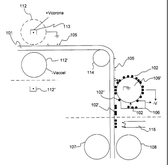
Figure 1 depicts an overview of a portion of an apparatus 100 configured to
establish conductive patterns 99 on a planar insulating substrate 101 wherein
the
patterns 99 are shown in accordance with an embodiment of the invention.
5 Various embodiments of the invention are based on (micro)particles 102
(not
shown in the figure 1), which can be deposited and permanently affixed to on
various substrates 101, at the same time increasing the conductivity of the
pattern
99 being deposited. This is achieved by at least one module of the apparatus
100,
which is configured to establish a predefined pattern 99 on a planar
insulating
substrate 101 so that conductive particles 102 can gather according to the
predefined pattern 99. Furthermore at least one another module of the
apparatus
100 is configured to transfer the conductive particles to the planar
insulating
substrate 101, wherein the conductive particles 102 are arranged to gather
according to the predefined pattern. Furthermore a sintering module of the
apparatus 100 is configured to fuse the conductive particles 102 on the planar
insulating substrate 101, wherein the conductive particles 102 are arranged to
fuse
according to the predefined pattern 99 to establish a conductive plane 99' on
the
planar insulating surface 101. Depending on the deposition used, no
intermediate
stages are required (if particles deposited in dry form or a drying stage for
the
deposited material is employed (if particles deposited in a liquid
suspension)).
Various embodiments of the invention are suited inter alia for dry-state
conductive
(including semiconductive) particles 102, for example microparticles in powder
form. The conductive particles 102 may be metallic, polymeric, or a
combination
thereof. The resolution of the created structures may dependent on the
particle
size of the powdered material, whereas in the deposition and sintering
processes
the composition of the material is generally of importance.
The substrate 101 can be almost any insulating and planar sheet, web, or fiber
or
fibrous web or the like. Paper, board and polymer films (plastics) have been
found
to suit well for the process, but other similar non-conductive surfaces may be
also
used. Paper or board can be coated, uncoated, wood-free or wood-containing.
Multilayered substrates are also usable. Other possible substrates include for
example textiles, non-woven materials, circuit boards of electronics industry,
moulded articles, glass, construction materials, such as wallpapers and floor
coatings unfired and fired ceramics, (bio)polymer bases and composites. Each
one of the listed substrates has its own application areas and advantages. In
particular a further embodiment of the invention is suitable for substrate
that has a
CA 02723886 2010-11-09
WO 2009/135985 PCT/F12008/050256
6
shattering or deformation point below 300 C, in particular below 250 C, even
below 200 C, that is, at least various paper and plastic grades not
tolerating high
temperatures.
Figure 2a depicts a cross section view of a portion of an apparatus 100
configured
to establish a conductive pattern 99 on a planar insulating substrate 101,
wherein
conductive particles 102 are being gathered and attached to a coupling agent
103
on the substrate 101 in accordance with an embodiment of the invention. Figure
2a depicts an embodiment of the at least one another module configured to
transfer the conductive particles 102 to the planar insulating substrate 101,
wherein the conductive particles 102 are arranged to gather according to the
predefined pattern 99. A container 106 comprises the conductive particles 102.
The planar insulating substrate 101 comprises the coupling agent 103. In an
embodiment of the invention the coupling agent 103 may be adhesive or the
like.
The coupling agent 103 is situated so that the particles may attach to it.
Further-
more the coupling agent 103 establishes the predefined pattern 99 (not shown
in
figure 2) on the substrate 101 in the embodiment of figure 2a. The substrate
101
contains also charges, a negative charge 105 and a positive charge 104.
In a further embodiment the charges 104,105 are generally uniformly (not
shown)
established to the substrate 101. In this further embodiment the charges
attracts
by the electro-magnetic fields the particles 102 to the substrate 101. The
coupling
agent 103 takes care of the further attachment of the particles 102 to the
substrate
101, in a place on the substrate 101 where the coupling agent 103 is situated.
At
other locations, where there is no coupling agent 103, the particles do not
attach to
the substrate 101.
In an embodiment the charges 104,105 are established to the insulating
substrate
101 according to the predefined pattern 99. Therefore the charges 104,105 are
situated generally according to the predefined pattern 99. Furthermore the
locations of the charges 104 correspondences with the locations of the
coupling
agent 103.
The charges 104 attract the conductive particles 102 as shown by arrows in
figure
2a. The force of the electro-magnetic field draws the conductive particles 102
to
the coupling agent 103. The coupling agent 103 attaches the conductive
particles
102 to the substrate 101. The attachment can be performed while the substrate
101 is moving, even at relatively high speed.
CA 02723886 2010-11-09
WO 2009/135985 PCT/F12008/050256
7
Figure 2b depicts a cross section view of a portion of an apparatus 100
configured
to establish a conductive pattern 99' on a planar insulating substrate 101,
wherein
conductive particles 102 have been coupled to the substrate 101 before
sintering
in accordance with an embodiment of the invention. In the embodiment of figure
2b the conductive particles 102 are being attached and coupled to the
substrate
101 by the coupling agent 103. The sintering process in the embodiment
comprises sintering rolls 107 and 108 situated on opposite sides of the
substrate
101. Thus after the conductive particles 102 are transferred on the surface of
the
substrate 101, particles 102 are sintered to form continuous, conductive
structures
99' (not shown in figure 2b). The sintering occurs under temperature and
pressure,
preferably in a separate or semiseparate sintering nip, which are illustrated,
in
figure 2b for example. A separate sintering nip comprises two separate rolls
107,108, whereas a semiseparate sintering nip utilizes the electrode roll as a
counter-roll for the sintering roll (not shown). One or both of the rolls
107,108 is
heated in order to achieve the desired sintering temperature. Depending on the
chosen temperature, also a pressure sufficient to cause sintering to occur is
generated in the sintering nip. Alternatively instead of sintering in a roll
nip, belt or
long nip such as shoe-nip can be used. In these further embodiments the nip
length can be several millimetres, typically between 2-500 mm, and have
pressures varying between 10 ¨ 20 000 kPa. Configurations for heating uses
same principles as with roll nip systems described above. In the sintering the
desired conductive (including semiconductive, depending on the properties of
used material) surface pattern 99' is formed. Thereby the final chipset 99'
may be
established on the substrate 101.
Sintering system
In the sintering process the conductive particles 102 are sintered together to
form
a continuous, conductive structure 99'. The sintering procedure may utilize
simply
pressure and temperature (either in a roll or plate configuration). This is
used to
exceed the melting and sintering temperature of the used conductor material.
Either one of both of the rolls 107, 108, plates or belts in the sinter nip
may be
heated. The surface materials of the heated material should tolerate the
temperature used (e.g., 50 C ¨ 250 C) without significant deformation.
Possible
surface materials for the roll are e.g. tungsten carbide, hard chrome, PTFE
covers
and its derivatives and ceramic material with anti-sticking properties (low
surface
energy). The sintering may occur in direct contact with the heated roll 108 or
the
heat may be transferred through the substrate material (107). Also both
contacting
CA 02723886 2010-11-09
WO 2009/135985 PCT/F12008/050256
8
rolls 107,108 may be heated to increase heat transfer in the nip. For
improving the
affixation of the conductive particles 102 to the substrate 101, it is
preferred that at
least the roll 107 or plate coming into contact with the surface of the
substrate 101
not comprising the particle-formed pattern (second roll) is heated. The roll
108 in
contact with the powder (first roll) may be in considerably lower temperature,
even
unheated and cooled.
Figure 3 depicts a cross section view of a portion of an apparatus 100
configured
to establish a conductive pattern 99 on a planar insulating substrate 101,
wherein
electric field is used to transfer conductive particles 102 in accordance with
an
embodiment of the invention. The planar insulating substrate 101 comprises the
coupling agent 103, preferably situated on the surface of the substrate 101
facing
the conductive particles 102. The embodiment of figure 3 comprises an electric
roll
109. The electric roll 109 comprises poles 110 which are connected to a
voltage
source. On the opposite side of the roll a container 106 containing the
conductive
particles 102 is located. The substrate 101 is between these two. When the
pole
110 comes close to the substrate 101 as the roll 109 rotates, the force of the
electro-magnetic field starts to draw the conductive particles 102 so that the
conductive particles 102' comes to contact and attaches to the coupling agent
103,
thereby to the substrate 101. The poles 110' are too far away from the
conductive
particles 102 so that they do not draw the conductive particles 102,102'. In
the
embodiment of figure 3, the predefined pattern 99 may be established according
to
the location and the pattern of the poles 110 on the circle of the roll 109.
Further-
more or alternatively, the coupling agent 103 may be of the predefined
pattern.
Therefore the pattern is established according to the combination of both the
coupling agent 103 and the poles 110 or simply by the coupling agent 103.
Furthermore the roll 109 may be adapted to move to create a certain pattern 99
of
the attached particles 102' on the substrate 101. Even furthermore the poles
110
may be guided by controlling the voltage of the poles 110 to establish the
predefined pattern 99.
Figure 4a depicts a cross section view of a portion of an apparatus 100
configured
to establish a conductive pattern 99 on a planar insulating substrate 101,
wherein
a coupling agent 103 is transferred to the substrate 101 in accordance with an
embodiment of the invention. Figure 4a depicts two alternative ways of
transferring
the coupling agent 103 to the substrate 101. Cannon 111 shoots or sprays the
coupling agent 103 to the surface of the substrate 101. The cannon 111 may be
arranged to spray the coupling agent 103 according to the predefined pattern
99 or
CA 02723886 2014-12-11
9
by generally uniformly. Alternatively the coupling agent 103 may be
transferred to
the substrate 101 by a roll 112. The roll 112 transfers the coupling agent
from a
container 113 containing the coupling agent 103. The roll 112 may be
controlled to
move to create the pattern 99. Also the roll may contain a predetermined shape
or
ornaments, i.e. predetermined pattern, so as to create the pattern 99 on the
substrate 101.
Figure 4b depicts a cross section view of a portion of an apparatus 100
configured
to establish a conductive pattern 99 on a planar insulating substrate 101,
wherein
a mask 115 and a voltage source and drain 114,114' are used to create
predefined charges 104,105 to the substrate 101 in accordance with an
embodiment of the invention. The mask 105 is used in the embodiment to
establish the pattern 99 with the charges 105 on the substrate 101. The
substrate
101 is transferred between the voltage sources 114 and 114'. Thereby there is
an
electric voltage, which creates the charges 104,105 to certain positions to
the
substrate 101. The mask 115 is thereby used to create the charges 104,105
according to the predefined pattern 99.
Figure 4c depicts a cross section view of a portion of an apparatus 100
configured
to establish a conductive pattern 99 on a planar insulating substrate 101,
wherein
the predefined charges 104 attracts and gathers the conductive particles 102
to
the substrate 101 in accordance with an embodiment of the invention. The
substrate 101 moves besides the container 106 containing the conductive
particles
102. Generally the substrate 101 moves in relation to the container 106 so
that a
distance is substantially between the substrate 101 and the container 106. The
substrate 101 contains the charges 104 according to the predefined pattern 99.
The charges 104 attract the conductive particles 102 to the substrate 101. The
substrate contains the coupling agent 103 on the side facing the conductive
particles 102. Accordingly the conductive particles 102 gather towards the
charges
104 and are attached to the substrate 101 by the coupling agent 103.
Therefore,
the conductive particles 102 are attached to the substrate 101 according to
the
predefined pattern 99.
Figure 4d depicts a cross section view of a portion of an apparatus 100
configured
to establish a conductive pattern 99 on a planar insulating substrate 101,
wherein
the conductive particles 102 are coupled to the substrate 101 before sintering
in
accordance with an embodiment of the invention. In the embodiment of figure 4d
the substrate 101 contains the generally uniform layer of coupling agent 103.
The
conductive particles 102 have been transferred to the substrate 101 to
establish
CA 02723886 2010-11-09
WO 2009/135985 PCT/F12008/050256
the predefined pattern 99. Otherwise the embodiment of figure 4d is similar to
the
embodiment of figure 2b.
Figure 5 depicts a cross section view of an apparatus 100 configured to
establish
a conductive pattern 99 on a planar insulating substrate 101 in accordance
with an
5 embodiment of the invention, wherein the coupling agent 103 is spread
according
to the predefined pattern 99 to the substrate 101 and electric roll 109' is
used. In
the embodiment of figure 5 the substrate 101 contains the coupling agent 103
as
predefined pattern 99. Thus the coupling agent 103 has been spread to the
substrate 101 so as to create the predefined pattern 99. The substrate 101
moves
10 forwards. The roll 109' rotates. The roll 109' contains a voltage source
+V. The roll
109" contains a voltage drain ¨V. Thereby the roll 109' gathers and attracts
conductive particles 102 from the container 106 to the surface of the roll
109',
when the roll 109' rotates. When the roll 109' rotates and the substrate 101
moves,
the conductive particles 102 come into contact with the coupling agent 103.
The
conductive particles 102 are attached to the coupling agent 103. Therefore the
conductive particles 102 establish the predefined pattern 99 on the surface of
the
substrate 101. Those conductive particles 102 that do not come into contact
with
the coupling agent 103 are not attached to the substrate 101 but remain on the
surface of the roll 109'.
Figure 6 depicts a cross section view of an apparatus 100 configured to
establish
a conductive pattern 99 on a planar insulating substrate 101 in accordance
with an
embodiment of the invention, wherein electric rolls 112,112',112" are used to
create charged patterns 99,105 on the substrate 101 and to attach conductive
particles 102 to the substrate 101 accordingly. Electric roll 112 contains a
voltage
source 113 to create +Vcorona voltage. The roll 112 contains a mask also so as
to
establish the pattern 99 by the charges 105. There can be two or more
alternatives
to the corona voltage such as 112' ¨Vaccel or a voltage drain 112". The mask
is
designed so that according to the predefined pattern of the mask the charges
105
are created on the substrate 101 accordingly. Thus the mask and the charges
105
create the predefined pattern 99 in the embodiment of figure 6. The embodiment
of figure 6 contains also electric roll 109'. In the embodiment of figure 6
the
substrate 101 does not contain the coupling agent 103. The substrate 101 moves
forwards and the rolls rotate. The roll 109' may contain a ground. There is
further-
more a drain ¨V to create the electric field. Thereby the roll 109' gathers
and
attracts conductive particles 102 from the container 106 to the surface of the
roll
109', when the roll 109' rotates. When the roll 109' rotates and the substrate
101
CA 02723886 2010-11-09
WO 2009/135985 PCT/F12008/050256
11
moves, the conductive particles 102 come into contact with the charges 105.
The
conductive particles 102 are attached to the substrate 101 by the charges 105.
Therefore the conductive particles 102 are attached on the substrate 101. The
conductive particles 102 establish the predefined pattern 99 on the surface of
the
substrate 101 in accordance with the pattern of the charges 105. Those
conductive particles 102 that do not come into contact with the charges 105
are
not attached to the substrate 101 but remain on the surface of the roll 109'.
The
sintering portion contains a heater 115, for example a radiator /IR.
Furthermore the
sintering portion contains also rolls 108 and 107. The sintering process may
operate generally similarly as in the embodiments of figures 2b and 4d.
Conductive particles
As discussed above some embodiments of the invention use conductive particles
102. A non-limiting example of the conductive particles is metallic
microparticles.
For a further embodiment, low melting point metals and metal alloys are
applied.
Especially tinbismuth alloy is verified to be suitable for the application. In
this
context, low melting point metals and alloys include materials having melting
points of less than 300 C, typically 50-250 C, in particular 100-200 C.
Suitable
metals include, e.g. tin, bismuth, indium, zinc, nickel, or similar. The
mentioned
metals are also preferred components of suitable alloys for further
embodiment, as
they have the capability of creating low melting point alloys. For example,
tin-bis-
muth, tin-bismuth-zinc, tin-bismuth-indium or tin-bismuth-zinc-indium in
different
ratios has proven advantageous in further embodiments of the invention.
Changing the ratios of these metals in the alloy can considerably change the
melting behaviour of the alloy. Tin-containing alloys, where the ratio of tin
in the
alloy is 20-90 wt-%, preferably 30-70 wt-%. The composition 15.6 wt-% of tin
36.1
wt-% of bismuth and 48.3 wt-% on indium results in a melting point of as low
as
59 C. Hence, really low-temperature applications are possible.
The size of the conductive particles, for example of metal or metal alloy
particles,
may be between 0.5 (or lower) and 100 pm (even higher), in 5 very high-
resolution
applications sometimes between 1 and 20 pm. The particles may comprise
essentially 100% of metal. That is, no auxiliary agents are needed contained
in the
particles, mixed in the powder or applied in advance on the substrate order to
carry out the further embodiments.
CA 02723886 2010-11-09
WO 2009/135985 PCT/F12008/050256
12
Other materials
In a further embodiment conductive polymers, such as polyaniline (PANI),
poly(3.4-ethylenedioxythiophene) (PEDOT), may be also used in the deposition
as
conductive particles, however the infusible nature of conducting polymers sets
challenges to sintering of materials. Basically, polymer with intrinsic
conductivity
does not melt or dissolve in any ordinary solvents. However, they have
degradation well above 200 C enabling them to be blended with various
synthetic
polymers such as polypropylene (PP), polyethylene (PE), polyethylene-CO-
methylacrylate (EMA), ethylene-propylene-diene terpolymer (EPDM) etc. These
composite materials have still conductivity of semiconductor level.
Particles container
Some embodiments of the invention use the particles container 106. An example
of the particles container may be a powder container or the like. The housing
of
the container 106 may be brought in contact with insulating structure,
particles or
surfaces, through which they attain charge. After this they are transferred on
the
transfer roll surface, by means of an electric field, for example. Usually a
certain
threshold voltage is required in order for the charge to distribute evenly to
the
particles in the particle carrier. The level of the threshold voltage depends
on the
type of particles. In some example tin-bismuth alloy typically has a voltage
of
about 200 V.
In a further embodiments in the container 106 fluidization is applied in order
to
create homogonous dispersions. This ensures even transfer and deposition of
particles to the transfer roll. Fluidisation can be made with air, mechanic
vibration
and by using repulsive electrostatic forces (with conductive particles).
Roll
Some embodiments of the invention use various rolls such as references
109,112.
The transfer roll may be electrically passive. The transfer roll may comprise
electrodes, which are in different potential than the particle deposited on
the
surface of the transfer roll. This potential difference may be created also
with
different surface charges in surface of roll, belt or like. The electric field
between
the container and the transfer roll is created to these electrodes. When an
electric
field is formed between the container (and conductive particles in it) and
transfer
roll, the charged particles transfer due to the electric field to the surface
of the
transfer roll.
CA 02723886 2010-11-09
WO 2009/135985 PCT/F12008/050256
13
Electrode roll
Some embodiments of the invention use roll 109,112, which is being
electrified.
The electrode in its simplest form is roll comprising a metal roll, which is
insulated
from the other system components and is in opposite potential to the charged
particles. The purpose is to create an electric field between the transfer
roll (and
with the particles on its surface) and the electrode roll for enabling
transfer of the
particles 102 to the surface of the substrate 101. In addition to this in
particle
transfer corona charging can be used to create a potential difference between
the
charged particles and the substrate. The opposite side of the substrate can be
charged with ions from corona charging and the other side of the substrate is
in
contact or in close proximity to charged particles and thus particle transfer
occurs.
Detach system
After the particles 102 have been transferred to the substrate 101 surface
there
may be need for detachment of the substrate 101 and the particles 102 from the
roll. Depending on the dielectric properties (both volume and surface
resistivity) of
the substrate 101, tix particles have a tendency to sustain the electrostatic
force
towards the electrode roll 109. This is caused by the potential difference
between
the particles 102 and the roll 109. To decrease the electrostatic force
between the
particles and the electrode roll 109, several actions can be made. First, the
moisture content of the web with fiber-based materials (paper and board) can
be
increased to enable charge transfer from the particle to the web with fiber-
based
and polymer films or the like. Second, an alterative current ionizer can be
used to
neutralize the charges of the particles. Third, the potential difference may
be
arranged to remain stable until the charge of the particles decays (for
example by
allowing the web be in contact with the electrode roll for a longer period).
Fourth,
the particles may be sintered while still in contact with the electrode. When
paper
or board is used as a substrate and a moisture-dependent detaching is
utilised,
the relative humidity of the process environment is preferably about 20-90%,
typically 30-60%. This relative humidity means for example paper moisture
contents between 2-20 /0. This provides the charged particles a suitable
charge
decay time for the detaching.
Ramifications and Scope
Although the description above contains many specifics, these are merely
provided to illustrate the invention and should not be construed as
limitations of
CA 02723886 2014-12-11
. .
14
the invention's scope. It should be also noted that the many specifics can be
combined in various ways in a single or multiple embodiments. Thus it will be
apparent to those skilled in the art that various modifications and variations
can be
made in the apparatuses and processes of the present invention. Therefore, the
scope of the claims should not be limited by the specific embodiments
disclosed
herein, but should be given the broadest interpretation consistent with the
description as a whole.