Note: Descriptions are shown in the official language in which they were submitted.
CA 02724184 2010-11-12
TITLE OF THE INVENTION
ANTENNA DEVICE
BACKGROUND OF THE INVENTION
Field of the Invention
[0001 ] The present invention relates to an antenna device that can be
advantageously
used in a wireless communication technology such as a keyless operation system
for an
automobile and the like.
SUMMARY OF THE INVENTION
[0002] In recent years, antenna devices using linear elements have been
investigated
for the purpose of use in wireless communication, such as in a keyless
operation system
for an automobile. Conventionally, a monopole antenna having a length 1/4 that
of the
working wavelength of the antenna with respect to the ground plane and in
which a wire
element is disposed is generally used as an antenna device that uses linear
elements.
However, because this monopole antenna is large and tall overall, inverted-L
antennas
have been developed in which this monopole antenna is folded at an
intermediate point
to reduce the size and height.
[0003] Furthermore, in this inverted-L antenna, matching a 50 0 power feed
line is
very difficult because the reactance, which is determined by the length of the
horizontal
portion of the antenna element that is parallel to the ground plane, is the
capacitance,
and is a large value. Thus, conventionally, in order to facilitate matching
between an
antenna element and a 50 Q power feed line, what is referred to as an inverted-
F
antenna has been proposed. This inverted-F antenna is one in which a stub is
provided
that connects the ground plane and the radiation element near the power feed
point that
is provided at an intermediate location on the antenna element. Thereby, the
1
CA 02724184 2010-11-12
capacitance due to the reactance is neutralized, and matching a 50 0 power
feed line is
facilitated. For example, in Japanese Laid-Open Patent Application No. 2006-
197528,
an inverted-F antenna has been proposed that is applied to a folding portable
wireless
device, and provides an antenna element that is disposed on a printed wiring
substrate
and is folded perpendicular to a flexible flat cable that is connected to the
printed wiring
substrate. In this inverted-F antenna, the antenna element is folded in a
vertical
direction with respect to the printed wiring substrate.
[0004]
[Patent Literature I ] Japanese Patent Application Laid-Open No. 2006-197528
[0005] However, in the above conventional technology as well, the following
problems remain.
Specifically, in the conventional antenna, in the case in which the various
arrangement conditions are to be changed, the polarization (vertical and
horizontal
polarization) is designed with respect to the principal polarization as
required by the use
conditions, and due to being dependent thereon, handling polarization
improvements
using the same antenna profile is difficult. Thus, methods in which design
changes are
made to the antenna profile in order to improve polarization have been
considered, but
there are limits to design changes due to dependency on the size of the case
and there
are frequently difficulties in terms of the cost of producing metal molds and
the like.
Thus, a method in which a metal plate is disposed to change the polarization
forcibly
has been considered, but there the drawbacks that directionality is limited,
antenna
characteristics deteriorate, and the polarization cannot be easily improved.
In addition, in the case of the technology disclosed in Japanese Laid-Open
Patent Application No. 2006-197528, the characteristics are improved by
folding the
2
CA 02724184 2010-11-12
element in a length or width direction with respect to a flexible cable, but
because the
improvements in characteristics are dependent on the surrounding environment,
the
polarization and directionality cannot be improved, and downsizing and
increasing the
thinness are difficult. From the above point of view, in the case in which the
arrangement conditions are changed in the conventional technology, in the same
antenna, substrate, and case, there are the drawbacks that improving the
polarization,
obtaining high gain, downsizing, and increasing thinness are difficult.
[0006]
In consideration of the above described problems, it is an object of the
present
invention to provide an antenna device that improves the polarization of the
same
antenna and substrate and the like and can realize a high gain and downsizing
even in
the case in which the arrangement conditions change.
[0007]
The present invention uses the following structure to solve the problems
described above. Specifically, the antenna device of the present invention
provides a
first ground area on which a power feed component that is electrically
connected to the
power feed point of a wireless circuit is provided and that is formed by a
conductor; a
second ground area that is provided along the outer periphery of the first
ground area so
as to exclude a portion of the periphery thereon and that is formed by a
conductor; a
boundary between the first ground area and the second ground area; an antenna
element
that is electrically connected to the power feed point and is erected on the
first ground
area; and a ground connection component that locally electrically connects the
first
ground area and the second ground area. The antenna element is characterized
in
3
CA 02724184 2010-11-12
providing a raised component that rises from the first ground area and an
element
component that extends directly above the second area from the raised
component.
[0008] Because this antenna device provides a ground connection component that
locally electrically connects the first ground area and the second ground
area, and the
antenna element includes a raised component that rises from the first ground
area and an
element component that extends directly above the second ground area from the
upper
end portion of the rising area, high frequency current (current distribution)
that flows to
the antenna element, the first ground area, and the second ground area can be
adjusted
depending on the local connection position, and the polarization of the
antenna overall
can be improved. That is, a ground area that is divided into a plurality of
parts is
provided, and the characteristics of the desired polarization can be improved
without
changing the antenna element based on the dispositional relationship between
these
ground elements and the antenna element.
Note that the above term "boundary" denotes (electrically divided) portions at
which the first ground area and the second ground area are not electrically
connected.
Specifically, this "boundary" is an area or space at which the conductor of
the first
ground area and the conductor of the second ground area are not linked
together, and
denotes an electrically insulated range that is interposed between the first
ground area
and the second ground area.
In addition, providing the above "locally electrically connected ground
connection component" denotes that there is a location (the ground connection
component) that electrically connects the first ground area and the second
ground area
by crossing over the "boundary".
4
CA 02724184 2010-11-12
[0009] In addition, the antenna device of the present invention provides a
substrate on
which a ground pattern that is divided into the first ground area and the
second ground
area is provided.
A ground pattern that is provided on a substrate frequently naturally has
large
in size and is integrated from the viewpoint of improving the antenna gain.
Thus, in
the present invention, because a boundary for efficiently dividing the ground
pattern of
the substrate for the antenna element is provided and the frequency current
flowing to
the antenna element and the ground pattern is adjusted, the polarization of
the antenna
overall can be improved by making an efficient connection method.
[0010] In addition, the antenna device of the present invention provides a
first
substrate on which the first ground area is provided and a second substrate on
which the
second ground area is provided, and the first substrate and the second
substrate are
disposed such that the boundary is interposed therebetween.
Specifically, in this antenna device, because the first substrate and the
second
substrate are disposed such that the boundary is interposed therebetween, by
providing
the first ground area and the second ground area on separate substrates, an
arrangement
becomes possible in which one can be easily be replaced with another having a
separate
shape. For example, by using a general use substrate for one and using a
replacement
substrate for the other, a variety of shapes can be easily used.
[0011] In addition, in the antenna device of the present invention, the
boundary is
perpendicular to the element component at least at one location in a plan view
from
above the first ground area and the second ground area. Specifically, in this
antenna
device, because the boundary is perpendicular to the element component at
least at one
CA 02724184 2010-11-12
{
location in a plan view from above the first ground area and the second ground
area, the
current distribution can be most effectively adjusted.
[0012] In addition, in the antenna device of the present invention, the
boundary
divides the first ground area and the second ground area in proximity to the
power feed
point. Specifically, in this antenna device, because the boundary divides the
first
ground area and the second ground area in proximity to the power feed point, a
current
distribution can be more robustly adjusted.
[0013] In addition, in the antenna device of the present invention, the ground
connection component is provided at a proximate position near the power feed
point.
Specifically, in this antenna device, because the ground connection component
is
provided at a proximate position near the power feed point, when the principal
polarization is made the horizontal polarization, the effect of the
improvement of the
horizontal polarization can be more robustly obtained.
[0014] In addition, in the antenna device of the present invention, the ground
connecting component is provided at a distant position most separated from the
power
feed point. Specifically, in this antenna device, because the ground
connecting
component is provided at a distant position most separated from the power feed
point,
when the principal polarization is vertical polarization, the effect of the
improvement of
the vertical polarization can be more robustly obtained.
[0015] In addition, in the antenna device of the present invention, the ground
connection component is provided at an intermediate position on the boundary.
Specifically, in the antenna device, because the ground connection component
is
provided at an intermediate position on the boundary, in the case in which
both
6
CA 02724184 2010-11-12
horizontal polarization and the vertical polarization are necessary, the
effect of a
significant improvement of both polarizations can be obtained.
[0016] According to the present invention, the following effects are exhibited
According to the antenna device of the present invention, because a ground
connection component that locally electrically connects the first ground area
and the
second ground area is provided, and the antenna element includes a raised
component
that rises from the first ground area and an element component that extends
directly
above the second ground area from the upper end portion of the raised
component, the
high frequency current that flows to the antenna element, the first ground
area, and the
second ground area can be adjusted depending on the local connection position,
and the
polarization of the antenna overall can be improved. Specifically, even in the
case in
which the arrangement conditions are changed, based on the dispositional
relationship
between the above connection positions and the antenna element, the
polarization can
be improved, and increased gain and downsizing can be realized without
changing the
antenna element. Therefore, the antenna device of the present invention is
advantageous for any wireless communication system that is mounted on a
vehicle or
the like, and in particular, a reception antenna device, a transmission
antenna device, or
a transmission and reception antenna device used in a wireless operation
system.
BRIEF DESCRIPTION OF THE DRAWINGS
[0017]
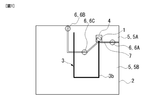
FIG. 1 is a simple plan view that shows the antenna device of a first
embodiment of the antenna device of the present invention.
FIG. 2 is a simple perspective view that shows the antenna device of the first
embodiment.
7
CA 02724184 2010-11-12
FIG. 3 is an explanatory drawing using an equivalent circuit that shows the
antenna device of the first embodiment.
FIG. 4 is a graph that shows, in a first embodiment, a radiation pattern in
the
case in which the ground connection component is provided at a proximate
position
near the power feed point in the first embodiment.
FIG. 5 is a graph that shows, in the first embodiment, a radiation pattern in
the
case in which the ground connection component is provided at a distant
position far
from the power feed point.
Fig. 6 is a graph that shows, in the first embodiment, a radiation pattern in
the
case in which the ground connection component is provided at an intermediate
position
on the boundary.
FIG. 7 is a graph that shows, in a first embodiment, the radiation pattern in
the
case in which the ground connection component is provided at three locations:
at a
proximate position near the power feed point, at a distant position far from
the power
feed point, and an intermediate position on the boundary.
FIG. 8 is a graph that shows, in a first embodiment, a comparison of maximum
gain for horizontal polarization and vertical polarization for the arrangement
positions
of the ground connection components.
FIG. 9 is a simple plan view that shows an antenna device of a second
embodiment of the antenna device according to the present invention.
DESCRIPTION OF THE EMBODIMENTS
[0018] Below, a first embodiment of the antenna device according to the
present
invention will be explained with reference to FIG. I to FIG. 8,
8
CA 02724184 2010-11-12
[0019] The antenna device of the present embodiment is a wireless
communication
system that is mounted, for example, in an automobile or the like, and in
particular, is a
reception antenna device, a transmission antenna device, or a transmission and
reception
antenna device used in a keyless operation system. As shown in FIGS. 1 to 3,
the
antenna device provides a first ground area 5A on which a power feed point I
that is
electrically connected to a 50 0 power feed line (power feed component of the
wireless
circuit; not illustrated) and is formed by a conductor such as copper foil or
the like; a
second ground area 5B that is formed by a conductor such as copper foil or the
like
along the outer periphery of the first ground area 5A so as to exclude a
portion thereof;
a boundary 7 between the first ground area 5A and the second ground area 5B;
an
antenna element 3 that is electrically connected to the power feed point l and
is erected
above the first ground area 5A; and a ground connection component 6 that
locally
electrically connects the first ground area 5A and the second ground area 5B.
[0020] In addition, the antenna device provides a substrate 2 on which a
ground
pattern 5 is provided, which is divided in to the first ground area 5A and the
second
ground area 513; and a matching circuit component 4, which is electrically
connected to
the power feed point I and the antenna element 3, provided on the substrate 2,
and that
matches the reactance of the antenna element 3 and the power feed line.
[0021] Specifically, this antenna device provides a substrate 2 on which a
power feed
point 1, to which a 50 0 power feed line (not illustrated) is electrically
connected, is
provided; an antenna element 3 that is electrically connected to the power
feed point 1
and is erected on the substrate 2; a matching circuit component 4 that is
electrically
connected to the power feed point 1 and the antenna element 3, erected on the
substrate
9
CA 02724184 2010-11-12
2, and matches the reactance of the antenna element 3 and the power feed line;
and a
ground pattern 5 that is provided on the substrate 2.
[0022] Note that the key operation system described above denotes a system
that
enables the locking or unlocking operation (what is referred to as a "keyless
entry
system") of the doors or tailgate and the like of an automobile and the
startup of an
engine and the like by carrying out a check of an ID code by wireless
communication
between the key and the receiving antenna device arranged on automobile main
body
side when a driver or the like simply approaches the vehicle within a wireless
operation
range carrying a key that is referred to as a "keyless operation key" and that
has a
wireless communication function.
[0023] The substrate 2 is, for example, a wired substrate or a circuit
substrate, and a
wireless communication circuit or an electronic control unit (ECU) or the like
(not
illustrated) including the matching circuit component 4, are formed on the
upper surface
and the lower surface thereof. Note that the antenna element 3 may also be
installed
on a side opposed to the surface on which the electronic control unit of the
substrate 2 is
mounted.
[0024] The antenna element 3 is formed by a conductive material such as copper
wire,
copper-clad wire, copper alloy wire (for example, brass) aluminum wire,
aluminum-clad
wire, or aluminum alloy wire or the like, having a length that is 1/4 or
another integer
fraction of that of the antenna working wavelength, and the thickness of the
wire is set
according to desired characteristics. In addition, the shape of the wire may
be a
cross-sectional profile of a circle, rectangle, or polygon or the like. In
consideration of
bending, a circular cross-section is preferable.
CA 02724184 2010-11-12
In addition, the antenna element 3 may be covered by an insulating layer on
the
outer periphery of the conducting materials (wire) described above.
[0025] This antenna element 3 includes a raised portion 3a that rises from the
first
ground area 5A and an element component 3b that extends directly above the
second
ground area 5B from the upper end portion of the raised portion 3a.
Specifically, this antenna element 3 includes a raised portion 3a that rises
from
the substrate 2, and an element 3b that bends from the upper end portion of
the raised
portion 3a and extends in an arbitrary direction within a plane parallel to
the substrate.
The element component 3b of the present embodiment is an open element that
bends or
curves back at an intermediate portion after extending in a direction in a
plane parallel
to the substrate 2 from the upper end portion of the raised portion 3a, and
forms
substantially square-C shape that extends along a direction opposite to the
first
direction.
[0026] Note that the element component 3b may extend in an arbitrary direction
after
extending directly over the second ground area 5B from the first ground area
5A, but
from the point of view of ease of formation of the antenna and stability of
the antenna
characteristics, as explained above, preferably the element component 3b is
formed so
as to extend in an arbitrary direction in a plane parallel to the substrate 2.
[0027] As described above, the ground pattern 5 is divided into the first
ground area
5A and the second ground area 5B at the boundary 7, which is a separation line
on the
substrate 2, and at the same time, includes a ground connecting portion 6 that
locally
electrically connects these ground areas 5A and 5B. In the present embodiment,
the
ground pattern 5 is divided into the first ground area 5A for analogue
circuits and a
second ground area 5B for digital circuits. In this ground pattern 5, the
second ground
11
CA 02724184 2010-11-12
area 5B is arranged along the outer periphery first ground area 5A so as to
exclude a
portion (the upper edge side and the right edge side in FIG. 1) of the outer
periphery.
Specifically, the second ground area 5B is disposed so as to leave open and
not
completely surround at least one portion of the outer periphery of the first
ground area
5A. Note that in the case in which the ground pattern 5 is divided at a
plurality of
locations, it is desirable that as large an area as possible for each of the
ground areas 5A
and 5B be ensured.
[0028] The boundary 7 is a line shaped or band shaped non-patterned portion
that
electrically divides the ground pattern 5 into the first ground area 5A and
the second
ground area 5B, except at a portion locally electrically connected by the
ground
connecting portion 6.
In addition, the first ground area 5A and the second ground area 5B are
divided
by the boundary 7 into such shapes as shown in FIG. I in conformity to the
shape of the
substrate 2. However, for example, the second ground area 5B may be divided
into an
alternative shape such as a rectangle by the boundary 7.
[0029] The boundary 7 intersects the element component 3b in a plan view from
above
the first ground area 5A and the second ground area 5B. In particular, the
boundary 7
is perpendicular to the element component 3b in a plan view from above the
first ground
area 5A and the second ground area 5B at least at one location, and preferably
the
ground pattern 5 is divided in proximity to the power feed point 1. In the
present
embodiment, in a plan view, the boundary 7 is perpendicular to the
substantially
C-shaped element component 3b at two at locations.
[0030] The matching circuit component 4 is a circuit structure including a n-
type LC
circuit formed by a plurality of inductors L or capacitors C or a T-type
circuit at a single
12
CA 02724184 2010-11-12
stage or a plurality of stages between the power feed point I and the antenna
element 3.
This matching circuit component 4 has the function corresponding to a portion
that
achieves matching from the power feed point to the stub in a conventional
inverted-F
antenna.
[0031] The ground connecting portion 6 is provided at least at one location
depending
on the necessary polarization, and, for example, in the case that the
principal
polarization is horizontal polarization, the ground connecting portion 6 is
provided at a
proximate position 6A near the power feed point 1, and in the case in which
the
principal polarization is vertical polarization, the ground connecting portion
6 is
provided at a distant location 6B most separated from the power feed point 1.
Furthermore, in the case in which both horizontal polarization and vertical
polarization
are necessary, the ground connecting portion 6 is provided at an intermediate
position
6C along the boundary 7.
Note that the terms "proximate" and "distant" with respect to the connection
position of the ground connection component 6 denote distances from the power
feed
point 1 that is electrically connected to the antenna element 3 on the
boundary 7.
[0032] In addition, passive elements such as generally used resistors,
capacitors, and
inducers and the like are used at the ground connecting portion 6.
Note that by using a variable resistor, a variable capacitor, or a variable
inducer
or the like as the ground connecting portion 6, flexible adjustment also
becomes
possible. In addition, a ground connecting portion 6 such as copper file or
the like
may be used.
13
CA 02724184 2010-11-12
[0033] Next, the results of measuring actual polarization and directionality
of the
antenna device of the present embodiment by varying the position of the ground
connecting portion 6 for will be explained.
[0034] First, FIG. 4 shows the result of measuring the radiation pattern for
the case in
which the ground connection component 6 is provided at the proximate location
6 near
the power feed point. As can be understood from this result, advantageous
results are
obtained for a radiation pattern whose principal polarization is horizontal
polarization,
has a toroidal directionality, and has a maximum gain of -11.63 dBi. In
addition, here
the maximum gain of the vertical polarization is a low value of -28.13 dBi.
[0035] In addition, FIG. 5 shows the result of measuring a horizontal
radiation pattern
of substrate 2 for the case in which the ground connection component 6 is
provided at
the distant position 6B far from the power feed point 1. As can be understood
from
this result, the principal polarization of the radiation pattern is vertical
polarization, and
thus, the principal polarization changes in comparison to the case in which
the ground
connection component 6 is provided at the proximate position 6A. Note that the
horizontal polarization having a toroidal directionality remains as-is, but
the maximum
gain becomes -19.28 dBi. In addition, in contrast, the maximum gain of a
vertical
polarization, which is the principal polarization, is -15.01 dBi, and a high
gain of 13 dB
is obtained in comparison to the case in which the ground connection component
6 is
provided at the proximate position 6A.
[0036] In addition, FIG. 6 shows the result of measuring the radiation pattern
for the
case in which the ground connection component 6 is provided at the
intermediate
position 6C of the boundary 7. As can be understood from this result, the
vertical
14
CA 02724184 2010-11-12
polarization and the horizontal polarization of the radiation pattern are both
substantially identical, and a directionality of -17 dBi is obtained at the
maximum gain.
In this manner, for the same antenna element 3, simply by changing only the
connection position of the ground areas 5A and 5B, the polarization can be
improved by
adjusting the gain of the vertical polarization, the horizontal polarization,
or both
polarizations
[0037] Note that FIG. 7 shows the results of measuring the radiation pattern
for the
case in which the ground connection component 6 is connected at all three
locations,
that is, the above proximate position 6A, the distant position 6B, and the
intermediate
position 6C. As can be understood from these results, the polarization
obtaining the
maximum gain, that is, the horizontal polarization when electrically connected
at the
proximate position 6A shown in FIG. 6, has a toroidal directionality and a
maximum
gain of -11.63 dBi, and thus, has characteristics similar to the state shown
in FIG. 4.
However, when compared to the radiation pattern in FIG. 4, an advantageous
result is
obtained in which the vertical polarization is improved and the maximum gain
is -21.02
dBi. That is, by combining the connection positions of the ground areas 5A and
5B
(the arrangement positions of the ground connection components 6), the high
frequency
current (current distribution) flowing to the antenna element 3 and the ground
pattern 5
can be adjusted, and the polarization of the antenna overall can be improved.
[0038] In addition, as quantitative evidence, a comparison of maximum gain is
shown
in FIG. 8. This is the result of extracting the maximum gain for each of the
horizontal
and vertical polarizations for each of the radiation patterns from FIG. 4 to
FIG. 6 and
comparing the positions of the ground connection component 6. As can be
understood
from this result, the horizontal polarization deteriorates as the position of
the ground
CA 02724184 2010-11-12
connection component 6 becomes more distant from the power feed point 1, and
the
vertical polarization improves as the position of the ground connection
component 6
becomes more distant from the power feed point 1. This means that the position
of the
ground connection component 6 is provided at the proximate position 6A near
the
power feed point 1 when the principal polarization is to be the horizontal
polarization;
the ground connection component 6 is provided at the distant position 6B far
from the
power feed point I in the case in which the principal polarization is to be
the vertical
polarization; and furthermore, the position of the ground connection component
6 is
provided at the intermediate point 6C of the boundary in the case in which
both
polarizations are necessary. Thereby, the polarization can be improved. Note
that
FIG. 8 is the result comparing the radiation pattern of the horizontal plane
of the
substrate 2, but in the case of the radiation pattern of the other planes, the
relationships
in FIG. 8 are reversed.
[0039] In this manner, the antenna device of the present embodiment provides a
ground connection component 6 that locally electrically connects the first
ground area
5A and the second ground area 5B, and the antenna element 3 includes a rising
area 3a
that rises from the first ground area 5A and an element component 3b that
extends
directly above the second ground area 5B from the upper end portion of the
rising
portion 3a. Thus, the high frequency current (current distribution) that flows
to the
antenna element 3 and the ground pattern 5 (first ground area 5A and second
ground
area 513) can be adjusted depending on the local connection position, and the
polarization of the antenna overall can be improved. This means that plural
divided
ground areas 5A and 5B are provided, and based on the positional relationships
between
16
CA 02724184 2010-11-12
the connection positions thereof and the antenna element 3, the
characteristics of the
desired polarization can be improved without changing the antenna element 3.
[0040] Frequently, the size of the ground pattern 5 provided on the substrate
2 was
naturally made large and integrated in consideration of improving the antenna
gain.
Thus, in the present embodiment, a boundary 7 for efficiently dividing the
ground
pattern 5 of the substrate 2 with respect to the antenna element 3 is
provided, and in
order to adjust the high frequency current that flows to the antenna element 3
and the
ground pattern 5, the polarization of the antenna overall can be improved by
an efficient
connection method.
[0041] In addition, because the boundary 7 is perpendicular to the element
component
3b in a plan view from above the first ground area 5A and the second ground
area 5B at
least at one location, the current distribution can be adjusted most
effectively.
Furthermore, because the boundary 7 divides the ground pattern 5 in proximity
to the power feed point 1, the current distribution can be adjusted more
robustly.
[0042] In addition, when the ground connection component 6 is provided at a
proximate position near the power feed point 1, in the case in which the
principle
polarization is horizontal polarization, the effect of an improvement in
characteristics
can be more robustly obtained.
In addition, when the ground connection component 6 is provided at a distant
position most separated from the power feed point 1, in the case in which the
principal
polarization is vertical polarization, the effect of an improvement in
vertical polarization
can be more robustly obtained.
In addition, when the ground connection component 6 is provided at an
intermediate position of the boundary 7, in the case in which both the
horizontal
17
CA 02724184 2010-11-12
polarization and the vertical polarization are necessary, the effect of an
improvement in
both polarizations can be more robustly obtained.
[0043] Next, a second embodiment of the antenna device according to the
present
invention will be explained with reference to FIG. 9. Note that in the
following
explanation of the embodiment, identical structural components explained in
the above
embodiment have appended identical reference numeral, and the explanation
thereof is
omitted.
[0044] The point of difference between the second embodiment and the first
embodiment is that in the first embodiment a first ground area 5A and a second
ground
area 5B that are divided from each other on one substrate 2 by the boundary 7
are
formed, whereas in contrast, the antenna device of the second embodiment, as
shown in
FIG. 9, provides a first substrate 22A on which the first ground area 25A is
provided
and a second substrate 22B on which a second ground area 25B is provided, and
the
first substrate 22A and the second substrate 22B are provided such that the
boundary 27
is interposed therebetween.
[0045] The antenna device of this second embodiment provides a square shaped
first
substrate 22A and a recessed second substrate 22B that is arranged along the
other three
edges excluding one edge on the outer periphery of the first substrate 22A.
Specifically, the antenna device of the second embodiment provides a square
first
ground area 25A formed on the first substrate 22A and a recessed second ground
area
25B that is formed on the second substrate 22B along the outer periphery of
the first
ground area 25A so as to exclude a portion of the outer periphery thereof.
18
CA 02724184 2010-11-12
[0046] Therefore, the boundary 27 that divides the first ground area 25A and
the
second ground area 25B is not a dividing line on the substrate, but rather is
a gap area
between the first substrate 22A and the second substrate 22B.
In this manner, in the second embodiment, because the first substrate 22A and
the second substrate 22B are disposed so as to surround the boundary 27, by
providing
the first ground area 25A and the second ground area 25B on separate
substrates, an
arrangement in which one is easily replaced by another having a different
shape
becomes possible. For example, by making one a general-use substrate and
making the
other a replacement substrate, a variety of shapes can be easily used.
[0047] Note that the present invention is not limited by the embodiments
described
above, but various modifications can be added within a range that does not
depart from
the spirit of the present invention.
[0048] For example, in the first embodiment, a ground pattern 5 is formed on
the
surface of a substrate 2, but there are cases in which a multilayer substrate
is used as a
substrate when designing an actual wireless circuit. In this case, the ground
pattern 5
may be designed on any layer, such as an inner layer pattern. Note that
ideally, the
ground pattern 5 is preferably designed on a component surface or solder
surface of the
surface of the substrate.
In addition, the antenna element 3 was formed by a conducting line made by a
copper wire or the like, but the antenna element 3 may be formed by other
conductors.
For example, an antenna element that has been stamped on a metal plate and
formed
into a band (the cross-sectional profile being rectangular) may be formed.
19