Note: Descriptions are shown in the official language in which they were submitted.
CA 02724212 2010-11-12
PCT/EP2009/055710 / 2008PO8828WO
1
Description
Sensor device
The invention relates to a sensor device for an image
recording apparatus for recording radiation by means of
sensors and to a method for recording an image.
Sensor arrangements consisting of sensor elements are provided
for example in electronic cameras. For example, an image is
projected onto a CCD (Charge Coupled Device) by way of a lens
system.
Due to the large number of sensor elements present on a CCD,
however, an image of said kind has a very high memory space
requirement. Furthermore a very high transmission capacity is
required for the transmission of the image data from the
camera in the case of a data processing unit.
In order to minimize the volume of data transmitted during the
transmission of the image the image data is therefore often
subjected to a data compression method. For example, the image
data is therein subjected to what is termed a wavelet
transform and subsequently compressed. Said wavelet transform
of the image data does not, however, make the data memory in
the camera superfluous or obsolete, since the recorded image
data must first be buffered in a data memory before the
wavelet transform is performed. Furthermore an additional
processor unit must be provided in order to perform the
wavelet transform, said processor unit increasing the
technical complexity of the camera while at the same time also
leading to an increased energy requirement.
CA 02724212 2010-11-12
PCT/EP2009/055710 / 2008208828WO
2
US 7,362,363 B2 therefore proposes a sensor arrangement which
already at the time of recording an image generates a
compressed representation of the image contents so that an
additional processor unit can be dispensed with by way of the
wavelet transform. For this purpose said known sensor
arrangement has a plurality of sensor elements whose measured
values are read with the aid of a readout means. In order to
perform an overall measurement a plurality of partial
measurements are performed in succession, a readout means
controlling the reading of the sensor elements in such a way
that in the respective partial measurements the measured
values of different sensor elements in each case are added and
subtracted.
However, this conventional sensor arrangement has the
disadvantage that the readout means requiring to be provided
in order to read out the measured values from the sensor
elements has a high degree of technical complexity since the
sensor or sensor arrangement must be variably wirable pixel by
pixel. The manufacture of a sensor arrangement of said kind,
in particular in the case of integration on a single chip, is
therefore very labor-intensive and expensive. Moreover the
complex readout means requires a great deal of space in the
case of integration on account of its complexity.
It is therefore an object of the present invention to provide
a sensor device for recording an image which provides a
compressed representation of the image contents and at the
same time has the lowest possible technical complexity.
This object is achieved according to the invention by means of
a sensor device having the features recited in claim 1.
CA 02724212 2010-11-12
PCT/EP2009/055710 / 2008P08828W0
3
The invention provides a sensor device having a plurality of
sensor layers arranged vertically one on top of the other,
each consisting of sensor elements, wherein coefficients of a
basis function of a detail plane are sensorically captured in
each sensor layer by means of the sensor elements, wherein the
sensor elements of the sensor layers are permanently wired and
in each case directly yield a measured value whose size
corresponds to a coefficient of the basis function.
An advantage of the sensor manufacture according to the
invention is that owing to the permanent wiring of the sensor
elements of the different sensor layers the circuit logic of
the sensor device is simplified by comparison with a
conventional sensor arrangement.
In the case of the sensor device according to the invention
the sensor elements are not variably wirable pixel by pixel,
but rather the sensor elements in the sensor layers or sensor
planes are permanently wired. The permanently wired sensor
elements of the different sensor layers are exposed
simultaneously. The incident light or, as the case may be, the
radiation is used simultaneously by all the sensor elements on
all the sensor layers or sensor planes.
In an embodiment variant of the sensor device according to the
invention the basis function is formed by means of a wavelet
basis function.
In an embodiment variant of the sensor device according to the
invention the sensor device provides an image recording of
radiation incident on a surface of a top sensor layer.
CA 02724212 2010-11-12
PCT/EP2009/055710 / 2008P08828W0
4
Said radiation can be any form of radiation, in particular
electromagnetic radiation, X-ray radiation, gamma radiation or
particle radiation.
The sensor device according to the invention is therefore
versatile and flexible and suitable for use in the widest
variety of application fields.
In an embodiment variant of the sensor device according to the
invention a resolution frequency of a sensor layer decreases
with increasing depth of the sensor layer starting from the
surface, and the resolution wavelength of a sensor layer
increases with increasing depth of the sensor layer starting
from the surface.
In an embodiment variant of the sensor device according to the
invention the resolution frequency of a further sensor layer
lying under a sensor layer is in each case half as great as
the resolution frequency of the sensor layer lying above.
In an embodiment variant of the sensor device according to the
invention the wavelet basis function used is a Haar wavelet
function.
In a further embodiment variant of the sensor device according
to the invention the wavelet basis function is a Coiflet
wavelet function.
In a possible further embodiment variant of the sensor device
according to the invention the wavelet basis function is a
Gabor wavelet basis function.
CA 02724212 2010-11-12
PCT/EP2009/055710 / 2008P08828W0
In a further embodiment variant of the sensor device according
to the invention the wavelet basis function used is a
Daubechies wavelet basis function.
In a further embodiment variant of the sensor device according
to the invention the wavelet basis function used is a
Johnston-Barnard wavelet function.
In a further possible embodiment variant of the sensor device
according to the invention the wavelet basis function used is
a bioorthogonal spline wavelet basis function.
In further possible embodiment variants further wavelet basis
functions not specifically cited above can be used.
In a possible embodiment variant of the sensor device
according to the invention the sensor elements are CCD sensor
elements.
In an alternative embodiment variant of the sensor device
according to the invention the sensor elements are CMOS sensor
elements.
In an embodiment variant of the sensor device according to the
invention the sensor layers consist of a radiation-permeable
material.
In an embodiment variant of the sensor device according to the
invention the total recording time of the sensor device
corresponds to the minimum exposure duration of the top sensor
layer at the highest resolution frequency and at the lowest
resolution wavelength.
CA 02724212 2010-11-12
PCT/EP2009/055710 / 2008208828W0
6
In an embodiment variant of the sensor device according to the
invention the minimum exposure duration of a sensor layer is
inversely proportional to the recording area of a sensor
element in the respective sensor layer.
In an embodiment variant of the sensor device according to the
invention the minimum exposure duration of a sensor layer
decreases exponentially with increasing depth of the sensor
layer starting from the surface of the sensor device.
In an embodiment variant of the sensor device according to the
invention the recording area of a sensor element of a sensor
layer increases exponentially with increasing depth of the
sensor layer starting from the surface of the sensor device.
In an embodiment variant of the sensor device according to the
invention the sensor device has N sensor layers arranged
vertically one on top of the other at a resolution of 2N
pixels.
The invention also provides an image recording apparatus
having a sensor device consisting of a plurality of sensor
layers arranged vertically one on top of the other, each
having sensor elements, wherein coefficients of a basis
function are sensorically captured by sensor elements in each
sensor layer and the sensor elements of the sensor layers are
permanently wired and in each case directly yield a measured
value whose size corresponds to a coefficient of the basis
function.
In an embodiment variant of the image recording apparatus
according to the invention the image recording apparatus also
has a signal processing device.
CA 02724212 2010-11-12
PCT/EP2009/055710 / 2008208828WO
7
In a possible embodiment variant the signal processing device
is a signal or data compression unit.
In a further embodiment variant of the image recording
apparatus the provided signal processing unit is a signal
filtering unit.
In a further possible embodiment variant the signal processing
device provided in the image recording apparatus is a signal
noise suppression unit.
In a possible embodiment variant of the image recording
apparatus the coefficients of the basis function captured by
sensor are buffered in a data memory.
In a further possible embodiment variant of the image
recording apparatus a calculation unit that is connected to a
screen is provided for calculating an inverse wavelet
transform.
The invention further provides a satellite having a sensor
device which has a plurality of sensor layers arranged
vertically one on top of the other, each consisting of sensor
elements, wherein coefficients of a basis function are
sensorically captured by the sensor elements in each sensor
layer, wherein the sensor elements of the sensor layers are
permanently wired and in each case directly yield a measured
value whose size corresponds to a coefficient of the basis
function, wherein the coefficients of the basis function
captured by sensor are transmitted via a radio interface of
the satellite to a signal processing device inside a ground
station.
CA 02724212 2010-11-12
PCT/EP2009/055710 / 2008208828W0
8
The invention further provides an X-ray machine having a
sensor device that has a plurality of sensor layers arranged
vertically one on top of the other, each consisting of sensor
elements, wherein coefficients of a basis function are
sensorically captured in each sensor layer by means of the
sensor elements, wherein the sensor elements of the sensor
layers are permanently wired and in each case directly yield a
measured value whose size corresponds to a coefficient of the
basis function.
The invention further provides a tomograph having a sensor
device that has a plurality of sensor layers arranged
vertically one on top of the other, each consisting of sensor
elements, wherein coefficients of a basis function are
sensorically captured in each sensor layer by means of the
sensor elements, wherein the sensor elements of the sensor
layers are permanently wired and in each case directly yield a
measured value whose size corresponds to a coefficient of the
basis function.
The invention further provides a method for recording an
image, wherein sensor elements of a plurality of sensor layers
arranged vertically one on top of the other sensorically
capture coefficients of a basis function, wherein the sensor
elements are permanently wired and in each case directly yield
a measured value whose size corresponds to a coefficient of
the basis function.
In an embodiment variant of the method according to the
invention the basis function used is formed by a wavelet basis
function.
CA 02724212 2010-11-12
PCT/EP2009/055710 / 2008P08828W0
9
Embodiment variants of the inventive sensor device and of the
inventive method for recording an image are described
hereinbelow with reference to the attached figures, in which:
Figure 1: shows a schematic sectional view through a sensor
device according to the invention;
Figure 2: shows a further sectional view to illustrate an
embodiment variant of the sensor device according
to the invention;
Figures 3A, 3B: are schematic representations serving to
explain the principle of operation of a sensor
element used in the sensor device according to the
invention in comparison with a conventional sensor
element. The sensor device shown measures a Haar
basis;
Figure 4: is a schematic representation of a possible
embodiment variant of the sensor device according
to the invention serving to explain its principle
of operation;
Figure 5: shows diagrams serving to explain a special
embodiment variant of the sensor device according
to the invention;
Figure 6: shows a block diagram serving to illustrate a
possible embodiment variant of an image recording
apparatus in which the sensor device according to
the invention is used;
CA 02724212 2010-11-12
PCT/EP2009/055710 / 2008P08828W0
Figure 7: shows a block diagram serving to illustrate an
exemplary embodiment of a satellite in which the
sensor device according to the invention is used.
As can be seen from Figure 1, the sensor device according to
the invention 1 has a plurality of sensor layers, 2-1, 2-2, 2-
3, 2-4, arranged vertically one on top of the other. In the
example shown in Figure 1 the sensor device 1 has N = 4 sensor
layers 2 arranged vertically one on top of the other. The
number N of vertically arranged sensor layers can vary. In a
sensor device 1 having a resolution of 2N pixels, preferably N
sensor layers 2 arranged one on top of the other are provided.
As shown schematically in Figure 1, radiation S impinges on
the top sensor layer 2-1 of the sensor device 1. The sensor
device 1 provides a recording of the incident radiation S. The
radiation S can be any form of radiation, in particular
electromagnetic radiation, X-ray radiation, gamma radiation or
particle radiation. Sensor elements that sensorically capture
coefficients c of a basis function BF are provided distributed
over the surface in each sensor layer 2-i. In this arrangement
the sensor elements of the sensor layers 2 are permanently
wired and in each case directly provide a measured value whose
size corresponds to a coefficient c of the basis function BF.
A wavelet basis function W-BF is preferably used as the basis
function BF. The sensor device 1 provides an image recording
of the radiation S impinging onto the surface of the top
sensor layer 2-1.
As indicated schematically in Figure 1, a resolution frequency
fA of a sensor layer 2 preferably decreases in this case with
increasing depth of the sensor layer starting from the surface
onto which the radiation S impinges. At the same time the
resolution wavelength XA of a sensor layer 2 increases with
CA 02724212 2010-11-12
PCT/EP2009/055710 / 2008PO8828WO
11
increasing depth of the sensor layer starting from the surface
onto which the radiation S impinges. In the exemplary
embodiment shown in Figure 1 the top sensor layer 2-1
therefore has the highest resolution frequency fA and at the
same time the lowest resolution wavelength AA. Conversely the
bottom sensor layer 2-4 has the lowest resolution frequency fA
and the highest resolution wavelength AA.
In a possible embodiment variant of the sensor device
according to the invention 1 the resolution frequency fA of a
further sensor layer 2-(i+l) lying under a sensor layer 2-i is
in each case half as great as the resolution frequency of the
sensor layer 2-i lying above it.
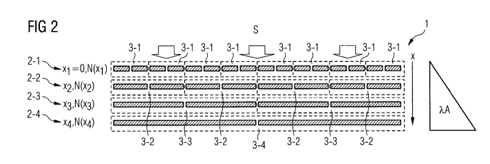
Figure 2 also shows a schematic sectional view through the
sensor device 1 depicted in Figure 1. As shown in Figure 2, a
plurality of sensor elements 3-i are disposed in each sensor
layer 2-i. In the example represented schematically in Figure
2 eight sensor elements 3-1 are contained in the top sensor
layer 2-1, four sensor elements 3-2 in the second sensor layer
2-2, three sensor elements 3-3 in the third sensor layer 2-3,
and a single sensor element 3-4 in the bottom sensor layer 2-
4. As can be seen from Figure 2, the size or, as the case may
be, recording surface area of the sensor elements 3-i
increases with increasing depth of the sensor layer. In a
possible embodiment variant of the sensor device according to
the invention 1 the recording surface area of a sensor element
3-i doubles in each further sensor layer starting from the top
sensor layer 2-1 down to the bottom sensor layer 2-N.
The sensor elements 3-i can be CMOS (Complementary Metal Oxide
Semiconductor) sensor elements. In an alternative embodiment
CA 02724212 2010-11-12
PCT/EP2009/055710 / 2008208828WO
12
variant the sensor elements 3-i are CCD (Charge Coupled
Device) sensor elements.
The sensor layers 2-i of the sensor device 1 consist of a
radiation-permeable material, the material being dependent on
a particular type of the radiation S that is to be recorded.
The absorption of the radiation S is described by means of an
exponential law, the Lambert-Beer law:
dN=_, r(x) => N(x) - - N(O)e-'
dx
The exposure duration is inversely proportional to the
recording area and decreases exponentially with the refinement
level or, as the case may be, depth of the sensor layer 2-i
starting from the surface.
In an embodiment variant of the sensor device according to the
invention 1 said absorption law is used for the purpose of
correctly exposing the sensor plane or sensor layers through
the suitable arrangement depth of the wired sensor layers 2-i,
the installation depth x of the sensor layers 2-i and the
photon energy for the exposure being calculated for the
purpose of dimensioning the sensor device 1.
In a possible embodiment variant of the sensor device 1
according to the invention the installation depth in a sensor
layer 2-i is yielded according to the Lambert law
M(x) = N(0)e-''X, where p is dependent on the material and the
frequency of the radiation to be measured. If the normalized
exposure is 1, the surface xl = 0 is exposed to the intensity
N(xl) = . The installation depth x2 for the second sensor
CA 02724212 2010-11-12
PCT/EP2009/055710 / 2008PO8828WO
13
layer 2-2 is yielded as a function of the material constant }i
corresponding to 1-4 of the intensity of the light:
N (x2) = 1/ = e-uX2
i.e. the installation depth for the second sensor layer 2-2 is
yielded as:
x2=- 1 In -
2
The installation depth x3 for the next sensor layer 2-3 is
yielded such that, as a function of the material constant u,
at least 1/8 of the light intensity or radiation intensity
still arrives there:
N (x3) = 1/8 = 1~ e ux3
Thus, the installation depth x3 of the third sensor layer 2-3
is yielded as follows:
X3 = - 1 In 4J .
Analogously, the installation depth of the fourth sensor layer
2-4 is yielded as:
N (x4) = 1/16 = 1~ e ux4
Thus, x4 = - 1 In
8
(I).
CA 02724212 2010-11-12
PCT/EP2009/055710 / 2008PO8828WO
14
The installation depth x4 of the lowest sensor layer 2-4 yields
the thickness of the sensor device 1 according to the
invention. The thickness of the sensor device 1 according to
the invention is therefore dependent on the constant p of the
material used for the sensor elements 3, which for its part is
determined by the radiation S that is to be captured.
In the sensor device 1 according to the invention, as shown in
Figure 2, a plurality of sequentially layered radiation-
permeable sensor elements of different sensor layers 2 are
exposed to the radiation S originating from the same radiation
source. The intensity of the radiation S in this case
decreases exponentially with a penetration depth x of the
radiation S into the sensor device 1. The sensor elements 3-i
of the different sensor layers 2-i are dimensioned such that
with increasing penetration depth they require exponentially
less radiation, i.e. the recording area of the sensor elements
3 increases with increasing layer depth xi of the respective
sensor layer 2-i, as shown schematically in Figure 2.
The sensor elements 3-i are radiolucent and connected one
after the other in series. The requisite minimum overall
recording time is in this case determined by the first sensor
layer 2-i or sensor plane. The total recording time of the
sensor device 1 corresponds to the minimum exposure duration
of the top sensor layer 2-1 having the highest resolution
frequency fA and the lowest resolution wavelength AA. Owing to
the fact that the sequentially connected linear sensor
elements 3-i are exposed simultaneously, half the exposure is
saved in the case of the sensor device 1 according to the
invention, since the incident radiation is used for all the
sensor layers 2-i. Owing to a differential measurement the
finest sensor plane or, as the case may be, the top sensor
CA 02724212 2010-11-12
PCT/EP2009/055710 / 2008P08828W0
layer 2-1 requires half the conventional exposure. The
absorbed residual radiation can be used by additional exposure
of the deeper-lying sensor planes or sensor layers. In this
case the full intensity and hence the same image quality is
added as follows:
~2 =1,
where i is the sensor layer 2-i.
Figures 3A, 3B schematically show the exposure measurement on
a sensor element 3-i of the sensor device 1 according to the
invention (Figure 3B) compared to the exposure measurement by
means of a conventional sensor element (Figure 3A). A
conventional exposure measurement takes twice as long as a
differential measurement for the same pixel size, because the
differential measurement uses two pixels for the exposure
measurement. The differential measurement can be performed
simultaneously in each sensor layer 2-i.
Figure 4 schematically shows the structure of a sensor device
1 according to the invention having three sensor layers 2-1,
2-2, 2-3. Radiation S, for example light radiation or particle
radiation, impinges onto the surface of the top sensor layer
2-1. As can be seen, the recording area of the single sensor
element within the bottom sensor layer 2-3 is considerably
larger than the recording area of the sensor elements
contained in the top sensor layer 2-1.
Figure 5 shows a diagram intended to illustrate a possible
embodiment variant of the sensor device 1 according to the
invention. In this embodiment variant a plurality of sublayers
CA 02724212 2010-11-12
PCT/EP2009/055710 / 2008P08828W0
16
are for their part provided in each sensor layer 2-i. For
example, as shown in Figure 5, three sublayers can be
provided. In this exemplary embodiment three differential
measurements are performed per sensor layer or sensor plane 2-
i, each in a quarter of the exposure time. Accordingly the
intensities of the recorded layers add up to 1:
3Y 4' =1 .
In the case of the sensor device 1 according to the invention,
as shown schematically in the exemplary embodiments according
to Figures 1 to 5, coefficients c of a basis function BF are
sensorically captured by means of the sensor elements 3-i of
each sensor layer 2-i. In a preferred embodiment variant said
basis function BF is what is termed a wavelet basis function.
In contrast to sine and cosine functions that are used in, for
example, the Fourier transform, wavelet functions exhibit
locality not only in the frequency spectrum, but also in the
time domain or, as the case may be, in the spatial domain,
i.e. they possess little scatter both in the frequency
spectrum and in the time domain or spatial domain. As a result
of the transformation the image data is brought into a form of
representation which offers advantages in subsequent
operations or signal processing steps. The direct generation
of wavelet coefficients by the sensor device 1 according to
the invention offers the advantage that no independent
processing unit or transformation unit needs to be provided
for performing wavelet transforms of said kind. In contrast to
periodic basis functions, as used in the Fourier transform,
local basis functions, such as wavelet basis functions, which
occupy finite intervals both in the time (spatial) and in the
frequency domain, are suitable in particular for signal
CA 02724212 2010-11-12
PCT/EP2009/055710 / 2008208828W0
17
discontinuities. Owing to the locality of the wavelet basis
functions, therefore, particularly steep edges of functions
can also be optimally represented. The basis functions include
what are termed scaling functions and wavelet basis functions.
Said functions have the fundamental characteristics of
orthogonality, i.e. the vectors of the functions are at right
angles to one another, thereby enabling a transformation and
an identical reconstruction. Owing to their finite extension
the basis functions enable image data to be analyzed without
window effects.
In an embodiment variant of the sensor device according to the
invention 1 the permanently wired sensor elements 3-i of the
sensor layers 2-i in each case form a measured value whose
size corresponds to a coefficient c of the basis function BF,
in particular a wavelet basis function.
In a possible embodiment variant of the sensor device
according to the invention 1 the wavelet basis function is a
Haar wavelet basis function.
In alternative embodiment variants other wavelet basis
functions can also be used, for example a Coiflet wavelet
basis function, a Gabor wavelet basis function, a Daubechies
wavelet basis function, a Johnston-Barnard wavelet basis
function or a biorthogonal spline wavelet basis function.
At a resolution of 2N pixels the sensor device 1 according to
the invention has N sensor layers 2-i vertically arranged one
on top of the other. For example, at a resolution of
1024 = 1010 pixels the sensor device 1 has a linear arrangement
of 10 sensor layers 2-i layered one on top of the other.
CA 02724212 2010-11-12
PCT/EP2009/055710 / 2008PO8828WO
18
In a possible embodiment variant of the sensor device 1
according to the invention a plurality of pixels in a sensor
layer 2-i are linked with or, as the case may be, multiplied
by prefactors. In this case the prefactors are yielded from
the construction of the wavelets. Sensor layers or sensor
planes can be economized by means of higher wavelets.
The material of the sensor elements 3 and the particle energy
are chosen such that the absorption coefficient has a suitable
value and the associated layer depth of the individual sensors
can be constructed.
In a possible embodiment variant sensors 3 can consist of
individual groups. In the sensor device 1 according to the
invention larger surface areas or recording areas of the
lower-lying sensor elements of the underlying sensor layers
are used in order to scatter the beams that are caused by
higher-lying sensors or sensor elements in above-lying sensor
layers 2.
In an embodiment variant of the sensor device according to the
invention 1 a Haar wavelet basis function is used as the basis
function BE.
The Haar wavelet basis function is defined by:
lfor0_<x<2
V /(X) = -1 for I <X<1 Ootherwise
The wavelet basis is then defined as
CA 02724212 2010-11-12
PCT/EP2009/055710 / 2008PO8828WO
19
41mn(X) = 2-m i!! (2-'x - n), m = 1, ..., L. n = Of ..., 2L-m - 1,
where n resolves the space, and m specifies the spatial
frequency or the level of detailing.
Functions can be represented as a wavelet series:
I z`-m-l l
f = fL+1 + (x)
m=L !=0
The function f (the image to be recorded) is given by 2L
discrete points:
f ={f},,i=0,...,2L -1
There are L layers. The wavelet coefficients of a detail plane
are measured in a layer m with m : 1 < m <- L:
cm,l, 1 = 0, ..., 2L-m -1
Figure 6 shows a block diagram of a possible embodiment
variant of an image recording apparatus 5 that includes a
sensor device 1 according to the invention. The sensor device
1 directly provides measured values whose size or height in
each case corresponds to a coefficient c of the implemented
basis function BF. Said coefficients c are output to a signal
processing device 6 inside the image recording apparatus 5. In
a possible embodiment variant the generated coefficients c are
initially stored temporarily in a buffer memory. The signal
processing device 6 can be a signal compression unit, a signal
filtering unit or even a signal noise suppression unit. The
processed coefficients c can then be supplied to a calculation
CA 02724212 2010-11-12
PCT/EP2009/055710 / 2008P08828W0
unit 7 which performs an inverse transform, in particular an
inverse wavelet transform. The transformation unit 7 provides
an image, displayable on the screen 8, of the radiation S
recorded by the sensor device 1. The image recording apparatus
5, as shown in Figure 6, can be a camera for example.
Furthermore the image recording apparatus 5 can also be an X-
ray machine for recording X-ray radiation S. A further
exemplary application of the apparatus 5 shown in Figure 6 is
a tomograph.
Figure 7 shows a further exemplary application of the sensor
device according to the invention 1. In this exemplary
application the sensor device 1 is provided in a satellite 9
and provides coefficients c of a basis function BF to a
transmitter device 10 of the satellite 9 which transmits the
coefficients c via a radio interface to a receiver unit 11
inside a ground station 12. A signal processing device 13 can
be provided in the ground station 12 for the purpose of
processing the transmitted coefficients c. Said processed
coefficients can be subjected to an inverse transform by means
of a calculation unit 14 and displayed on a screen 15 of the
ground station 12.
By means of a layerwise arrangement of sensor groups or sensor
elements 3 the sensor device 1 according to the invention
successively utilizes a residual radiation.
The simultaneous exposure of the sensor groups offers in
particular the following advantages:
At the same radiation intensity and resolution the sensor
groups are exposed for a shorter exposure time.
CA 02724212 2010-11-12
PCT/EP2009/055710 / 2008208828W0
21
With the same exposure time and resolution the simultaneous
exposure of the sensor groups leads to a lower requisite
radiation intensity of the radiation S.
At the same radiation intensity and exposure the simultaneous
exposure of the sensor groups leads to a higher resolution.
The sensor device 1 according to the invention additionally
offers the advantage that a maximum resolution can always be
achieved through a sufficiently long recording or exposure
time.
Above all, the sensor device 1 according to the invention
offers the advantage that the required information or, as the
case may be, the image data is available or generated directly
in compact form and consequently a necessary memory space
requirement is minimized.
The memory device according to the invention additionally
offers a high degree of flexibility in terms of adaptation for
different fields of application.
In a possible embodiment variant known noise frequencies of
noise signal sources can be suppressed directly during the
recording of the image by selectively omitting or not
implementing sensor planes or sensor layers 2-i. The
measurement time or exposure time can be optimized during the
exposure independently of the location. Consequently the total
measurement time of the sensor device 1 does not have to be
predefined a priori.
CA 02724212 2010-11-12
PCT/EP2009/055710 / 2008208828W0
22
The sensor device 1 according to the invention also offers a
high recording dynamic, since differences in intensities are
measured, and not absolute values.
The sensor device 1 according to the invention is suitable for
the most diverse applications, for example for generating X-
ray photographs, for long-range reconnaissance applications
and applications in astrophysics, as well as for digital
photography.
The exemplary embodiments presented are suitable for
performing intensity measurements of the incident radiation.
If a color measurement is desired, in a possible embodiment
variant all the images can be recorded for the three primary
colors or a color dispersion is performed in some other way.
In a possible embodiment variant the same basis function BF is
used for each color. In an alternative embodiment variant a
different basis function, in particular also a different
wavelet basis function, can also be used for each color.