Note: Descriptions are shown in the official language in which they were submitted.
CA 02724223 2010-11-12
1
-
_
DESCRIPTION
Title of the Invention
CONDUCTIVE FILM, AND TRANSPARENT HEATING ELEMENT
Technical Field
The present invention relates to a conductive film that
can be used as a part of a defroster (defrosting device) or
a window glass for a vehicle, as a heating sheet for heat
generation under an electric current, or as an electrode for
a touch panel, an inorganic EL device, an organic EL device,
or a solar cell, and to a transparent heating element
containing the conductive film.
Background Art
A device described in Japanese Laid-Open Patent
Publication No. 2005-197234 has recently been proposed as an
electroluminescence device capable of large-area (e.g., 0.25
m2 or more) light emission with high luminance and long
lifetime.
Meanwhile, structures described in Japanese Laid-Open
Patent Publication Nos. 2007-026989 and 10-289602 have been
known as a vehicle light containing a conductive film
capable of preventing illuminance reduction of the light.
The illuminance of a vehicle light may be reduced due
to the following causes:
(1) adhesion and accumulation of snow on the outer
circumferential surface of the front cover,
(2) adhesion and freezing of rain water or car wash water on
the outer circumferential surface of the front cover, and
CA 02724223 2010-11-12
2
(3) progression of (1) and (2) due to use of an HID lamp
light source having a high light intensity even under low
power consumption (a small heat generation amount).
The structure described in Japanese Laid-Open Patent
Publication No. 2007-026989 is obtained by attaching a
heating element containing a transparent electricity
insulating sheet and a conductive pattern printed thereon to
a formed lens using an in-mold method. Specifically, the
conductive pattern of the heating element is composed of a
composition containing a noble metal powder and a solvent-
soluble thermoplastic resin.
The structure described in Japanese Laid-Open Patent
Publication No. 10-289602 is obtained by attaching a heating
element into a lens portion of a vehicle lamp. The lens
portion is heated by applying an electric power to the
heating element under a predetermined condition. The
document describes that the heating element comprises a
transparent conductive film of ITO (Indium Tin Oxide), etc.
Furthermore, a device described in Japanese Laid-Open
Patent Publication No. 2006-190585 has been proposed as a
dye-sensitized solar cell capable of reducing adverse
effects of reflected electromagnetic waves without
significant reduction of the power generation efficiency.
In addition, in the field of electromagnetic-shielding
films, Japanese Laid-Open Patent Publication No. 2004-221565
has disclosed a technology for determining a thickening
ratio of line intersections in a mesh to minimize PDP image
quality deterioration due to moire or the like.
Summary of Invention
CA 02724223 2010-11-12
3
-
In the heating element described in Japanese Laid-Open
Patent Publication No. 2007-026989, one conductive wire may
be arranged in a zigzag manner on a headlamp front cover or
the like to form a long conductive line in view of obtaining
a desired resistance value (e.g., about 40 ohm). However, a
potential difference may be disadvantageously generated
between adjacent conductive line portions to cause
migration.
In the heating element described in Japanese Laid-Open
Patent Publication No. 10-289602, the transparent conductive
film of ITO, etc. is used. The film cannot be formed on a
curved surface of a formed body by a method other than
vacuum sputtering methods. Thus, the heating element is
disadvantageous in efficiency, cost, etc.
In addition, since the transparent conductive film is
composed of a ceramic such as ITO, the film may be cracked
when a sheet on which the transparent conductive film is
formed is bent in an in-mold method. Therefore, the film
can hardly be used in a vehicle light front cover or the
like having the curved-surface body and the transparent
heater though it can be used in a window glass with
relatively less curved surface.
Thus, the conventional heating elements are less
versatile and exclusively used in a vehicle light front
cover, a window glass, etc.
In the case of using a conductive film as an electrode
of a touch panel, an inorganic EL device, or an organic EL
device, a conductive portion has to be formed in view of
light refraction and diffraction in the portion to prevent
glare caused by a backlight, etc.
CA 02724223 2010-11-12
4
The solar cell described in Japanese Laid-Open Patent
Publication No. 2006-190585 utilizes a transparent
conductive film of ITO, etc., thereby resulting in the same
problems as Japanese Laid-Open Patent Publication No. 10-
289602. Also, the electromagnetic-shielding film technology
described in Japanese Laid-Open Patent Publication No. 2004-
221565 still has room for improvement.
Under such circumstances, an object of the present
invention is to provide a conductive film and a transparent
heating element which is usable as a heat generating sheet
by applying electric current thereto, and can exhibit an
improved heat generation efficiency, can prevent glare
caused by a vehicle or outdoor light, and can be versatilely
used in a vehicle light front cover, a window glass, etc.
Another object of the present invention is to provide a
conductive film that can be used as an electrode of a touch
panel, an inorganic EL device, or an organic EL device to
prevent glare caused by a backlight, etc.
A further object of the present invention is to provide
a conductive film that can be used as an electrode of a
solar cell to shield electromagnetic waves and to lower the
surface resistance without reduction of the power generation
efficiency.
For the purpose of realizing a highly versatile
transparent heating element usable for a vehicle light front
cover, a building window glass, a vehicle window glass,
etc., the inventor has examined a conductive film according
to a comparative example having a plurality of conductive
portions and a plurality of opening portions, which provide
mesh shapes in combination. Specifically, the conductive
CA 02724223 2010-11-12
portions are formed in a straight line shape and are crossed
to form the mesh shapes in the conductive film.
When the heating wire is arranged in a zigzag manner in
the conventional structure, a potential difference is
5 generated between the adjacent conductive line portions to
cause migration disadvantageously. In contrast, when the
conductive portions are formed in the mesh shapes, the
adjacent conductive portions are intrinsically in the short-
circuited condition, and the migration is never a problem.
The conductive portions can be composed of a thin metal
wire or the like excellent in malleability and ductility,
and therefore can be formed along a three-dimensional curved
surface having a minimum curvature radius of 300 mm or less.
However, it has been found that in the conductive film
according to the comparative example, diffracted lights
generated in the ends of the straight conductive portions
interact with each other in diffraction points arranged
linearly on the intersections to emit an intense interfering
light. Also, on the conductive portions, diffraction points
are arranged linearly to emit an intense light, though the
light is weaker than the interfering light from the
intersections. Therefore, when the conductive film is
incorporated in a window glass, significant glare or the
like is disadvantageously caused due to the interference of
the diffracted lights.
Thus, in the present invention, the problem has been
solved by using the following structure.
[1] A conductive film according to a first aspect of
the present invention comprising a plurality of conductive
portions and a plurality of opening portions, wherein the
CA 02724223 2010-11-12
6
-
combination of the conductive portions and the opening
portions has mesh shapes, the conductive portions are formed
in a wavy line shape containing arcs extending in alternate
directions, and at least one of the arcs is disposed between
intersections.
In this structure, the conductive portions hardly have
a straight section, so that diffraction points are not
arranged linearly on the intersections of the conductive
portions, and an interfering light from the intersections
has a low intensity. The same phenomenon is caused on the
conductive portions, and also an interfering light from the
conductive portions has a low intensity. In the present
invention, the mesh shapes can prevent glare or the like
caused by the interference of the diffracted lights.
Therefore, the conductive film is suitable for a transparent
heating element to be incorporated in a window glass (such
as a building window glass or a vehicle window glass), a
vehicle light front cover, etc. The straight section may be
appropriately formed if necessary depending on the product
using the conductive film (such as the window glass or the
vehicle light front cover), the period or amplitude of the
wavy line shape, etc.
Furthermore, when the conductive film of the present
invention is used as an electrode of a touch panel, an
inorganic EL device, or an organic EL device, the conductive
film can prevent glare or the like caused by a backlight and
thus can prevent visibility deterioration of a displayed
image.
Furthermore, when the conductive film is used as an
electrode of a solar cell, the conductive film can act as an
CA 02724223 2010-11-12
7
electromagnetic-shielding film and can exhibit a low surface
resistance to prevent reduction of power generation
efficiency.
[2] A conductive film according to the first aspect,
wherein a pair of optional tangent lines, which are
positioned on the circumference line of each mesh shape
symmetrically about the central point of the mesh shape, are
parallel to each other.
[3] A conductive film according to the first aspect,
wherein the arcs have a central angle of approximately 900
,
and the number of the arcs on the circumference line of each
mesh shape is 2n (n = 1, 2, 3, .").
[4] A conductive film according to the first aspect,
wherein the arcs have a central angle of approximately 90 ,
and the number of the arcs on the circumference line of each
mesh shape is 4n (n = 1, 2, 3,
[5] A conductive film according to the first aspect,
wherein in a line connecting the central points of optional
adjacent two mesh shapes disposed along the arrangement of
the intersections of the conductive portions, the length of
a first line segment connecting the central point of one
mesh shape and the intersection is equal to the length of a
second line segment connecting the central point of the
other mesh shape and the intersection.
[6] A conductive film according to the first aspect,
wherein in a line connecting the central points of optional
adjacent two mesh shapes disposed along the extending
direction of one conductive portion, the length of a third
line segment connecting the central point of one mesh shape
and another conductive portion is equal to the length of a
CA 02724223 2010-11-12
8
fourth line segment connecting the central point of the
other mesh shape and the other conductive portion.
[7] A conductive film according to the first aspect,
wherein in a line connecting the central points of optional
adjacent two mesh shapes disposed along the extending
direction of one conductive portion, the length of a third
line segment connecting the central point of one mesh shape
and another conductive portion is different from the length
of a fourth line segment connecting the central point of the
other mesh shape and the other conductive portion.
[8] A conductive film according to the first aspect,
wherein the arrangement period of the arcs varies along the
extending direction of the conductive portion.
[9] A conductive film according to the first aspect,
wherein the arrangement period of the arcs between one
intersection and a first intersection adjacently disposed at
one side of the one intersection along the extending
direction of one conductive portion is different from the
arrangement period of the arcs between the one intersection
and a second intersection adjacently disposed at the other
side of the one intersection.
[10] A conductive film according to the first aspect,
wherein the arrangement period of the arcs between the one
intersection and a third intersection adjacently disposed at
one side of the one intersection along the extending
direction of another conductive portion is different from
the arrangement period of the arcs between the one
intersection and a fourth intersection adjacently disposed
at the other side of the one intersection.
[11] A conductive film according to the first aspect,
CA 02724223 2010-11-12
9
-
wherein the arcs have a central angle of 750 to 105 ,
preferably approximately 90 .
[12] A conductive film according to the first aspect,
wherein the conductive portions have a crossing angle of 90
in the intersections.
[13] A conductive film according to the first aspect,
wherein the conductive portions have a crossing angle of 0
in the intersections.
[14] A conductive film according to the first aspect,
wherein the wavy line shape has a constant period.
[15] A conductive film according to the first aspect,
wherein the wavy line shape has a constant amplitude.
[16] A conductive film according to the first aspect,
wherein the conductive film has a total light transmittance
of 70% or more but less than 99%.
[17] A conductive film according to the first aspect,
wherein the wavy line shape has a line width of 5 to 50 pm.
[18] A conductive film according to the first aspect,
wherein the distance between adjacent wavy line shapes is
150 to 2000 ilm.
[19] A conductive film according to the first aspect,
wherein the conductive portions contain a metallic silver
portion formed by exposing and developing a photosensitive
silver salt layer disposed on a transparent support.
[20] A transparent heating element according to a
second aspect of the present invention comprising a
conductive film according to the first aspect.
As described above, when the conductive film or the
transparent heating element of the present invention is used
as a heat generating sheet by applying electric current, it
CA 02724223 2015-01-30
,
,
can exhibit an improved heat generation efficiency, can
prevent glare caused by a vehicle or outdoor light, and can
be versatilely used in a vehicle light front cover, a window
glass, etc.
When the conductive film of the present invention is
used as an electrode of a touch panel, an inorganic EL
device, or an organic EL device, glare or the like caused by
a backlight can be prevented.
When the conductive film of the present invention is
used as an electrode of a solar cell, it can act as an
electromagnetic-shielding film and can exhibit a low surface
resistance to prevent reduction of the power generation
efficiency.
Accordingly, in one aspect the present invention resides
in a conductive film comprising a plurality of conductive
portions and a plurality of opening portions, wherein a
combination of the conductive portions and the opening portions
has mesh shapes, the conductive portions are formed in a wavy
line shape containing arcs extending in alternate directions,
at least one of the arcs being disposed between intersections,
and in a line connecting central points of adjacent two mesh
shapes disposed along an extending direction of one conductive
portion, a length of a line segment connecting the central
point of one mesh shape and another conductive portion is equal
to a length of a line segment connecting the central point of
the other mesh shape and the other conductive portion, and the
number of arcs on a circumference line of each mesh shape is 2k
(k = 1, 2, 3,...).
In another aspect, the present invention resides in a
conductive film comprising a plurality of conductive portions
and a plurality of opening portions, wherein the combination of
the conductive portions and the opening portions has mesh
shapes, the conductive portions are formed in a wavy line shape
containing arcs extending in alternate directions, at least one
of the arcs being disposed between intersections, and the
CA 02724223 2015-01-30
10a
number of arcs between one intersection and a first
intersection adjacently disposed at one side of the one
intersection along an extending direction of one conductive
portion is different from the number of arcs between the one
intersection and a second intersection adjacently disposed at
another side of the one intersection along an extending
direction of another conductive portion.
In yet a further aspect, the present invention resides in
a conductive film comprising a plurality of conductive portions
and a plurality of opening portions, wherein the combination of
the conductive portions and the opening portions has mesh
shapes, the conductive portions are formed in a wavy line shape
containing arcs extending in alternate directions, at least one
of the arcs being disposed between intersections, and the
conductive portions have a crossing angle of 00 in the
intersections, the mesh shapes are circles, and the circles
have the same size and are arranged in a matrix to form a mesh
pattern.
Brief Description of Drawings
FIG. 1 is a plan view partially showing a first
conductive film;
FIG. 2 is a cross-sectional view taken along the II-II
line of FIG. 1;
FIG. 3 is a plan view showing an example structure of a
first transparent heating element using the first conductive
film;
FIG. 4 is an explanatory view schematically showing a
mesh pattern of the first conductive film;
FIG. 5 is a plan view partially showing a second
conductive film;
FIG. 6 is a plan view showing an example structure of a
second transparent heating element using the second
conductive film;
FIG. 7 is an explanatory view schematically showing a
CA 02724223 2010-11-12
11
mesh pattern of a third conductive film;
FIG. 8 is a front view showing a product (conductive
sheet) using the third conductive film;
FIG. 9 is a back view showing the conductive sheet;
FIG. 10 is a top view showing the conductive sheet;
FIG. 11 is a bottom view showing the conductive sheet;
FIG. 12 is a left side view showing the conductive
sheet;
FIG. 13 is a right side view showing the conductive
sheet;
FIG. 14 is a perspective view showing the conductive
sheet;
FIG. 15 is a front view showing the use of the
conductive sheet;
FIG. 16 is an explanatory view schematically showing a
mesh pattern of a fourth conductive film;
FIG. 17 is an explanatory view schematically showing a
mesh pattern of a fifth conductive film;
FIG. 18 is an explanatory view schematically showing a
mesh pattern of a sixth conductive film;
FIG. 19 is an explanatory view schematically showing a
mesh pattern of a seventh conductive film;
FIG. 20 is an explanatory view schematically showing a
mesh pattern of an eighth conductive film;
FIGS. 21A to 21E are views showing the process of a
first production method for producing a conductive film
according to an embodiment of the present invention;
FIGS. 22A and 22B are views showing the process of a
second production method for forming the conductive film of
the embodiment;
CA 02724223 2010-11-12
12
_
FIGS. 23A and 23B are views showing the process of a
third production method for forming the conductive film of
the embodiment;
FIG. 24 is a view showing the process of a fourth
production method for forming the conductive film of the
embodiment; and
FIG. 25A is an observation photograph of Example 1,
FIG. 25B is that of Example 5, FIG. 25C is that of
Comparative Example 1, and FIG. 25D is that of Comparative
Example 2.
Description of Embodiments
Several embodiments of the conductive film and the
transparent heating element of the present invention will be
described below with reference to FIGS. 1 to 25D.
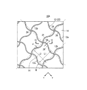
As shown in FIG. 1, a conductive film according to a
first embodiment (hereinafter referred to as the first
conductive film 10A) contains a plurality of conductive
portions 12 and a plurality of opening portions 14, and the
combination of the conductive portions 12 and the opening
portions 14 has mesh shapes M. Each mesh shape M is a
combined shape of one opening portion 14 and four conductive
portions 12 surrounding the opening portion 14.
The first conductive film 10A can be used as a part of
a defroster (defrosting device) or a window glass for a
vehicle. The first conductive film 10A can be used also in
a transparent heating element capable of heat generation by
applying electric current. As shown in FIG. 2, the first
conductive film 10A has a transparent film substrate 16, and
the conductive portions 12 and the opening portions 14
CA 02724223 2010-11-12
13
_
formed thereon. As shown in FIG. 3, when the first
conductive film 10A is used in a first transparent heating
element 18A, a first electrode 20a and a second electrode
20b are disposed on the opposite ends of the first
conductive film 10A (e.g., the right and left ends of FIG.
3), and electric current is applied from the first electrode
20a to the second electrode 20b. Thus, the first
transparent heating element 18A generates heat, whereby a
heating object that is brought into contact or equipped with
the first transparent heating element 18A (such as a
building window glass, a vehicle window glass, or a vehicle
light front cover) is heated. As a result, snow or the like
attached to the heating object is removed.
As shown in FIG. 1, the conductive portions 12 in the
first conductive film 10A have a mesh pattern 22 formed by
crossing a plurality of first thin metal wires 12a arranged
at a first pitch Li in one direction (the x direction of
FIG. 1) and a plurality of second thin metal wires 12b
arranged at a second pitch L2 in another direction (the y
direction of FIG. 1). The first pitch Li and the second
pitch L2 may be selected within a range of 150 !Am to 6000 !im
(6.0 mm). The line width d of each of the first and second
thin metal wires may be selected within a range of 5 pm to
200 Kr! (0.2 mm). It is to be understood that the line width
d may be selected within a range of 5 to 50 !Am to improve
the transparency.
The term "first pitch Li" is suitable for the first
thin metal wires 12a arranged at the constant distance.
However, the first pitch Li may vary between some of the
first thin metal wires 12a, and in this case the term
CA 02724223 2010-11-12
14
-
"distance between adjacent first thin metal wires 12a" is
more appropriately used. Also, the second thin metal wires
12b may be arranged in this manner. Thus, the distance
between adjacent first thin metal wires 12a and the distance
between adjacent second thin metal wires 12b are preferably
150 to 6000 pa, more preferably 300 to 1000 Krt.
The conductive portions 12 have the mesh pattern 22
containing a large number of lattice intersection points
(intersections 24) formed by the first thin metal wires 12a
and the second thin metal wires 12b. Each of the conductive
portions 12 is formed in a wavy line shape containing at
least one curve between the intersections 24.
Specifically, in the first conductive film 10A, the
wavy line shape contains arcs 26, and two arcs 26 extending
in alternate crest and trough directions are continuously
formed between the intersections 24. Each arc 26 has a
central angle of 75 to 105 , preferably approximately 90 .
The conductive portions 12 have a crossing angle of
approximately 90 . Though the preferred central angle and
the preferred crossing angle are represented by the term
"approximately 90 " in view of production tolerance, it is
desired that the central angle and the crossing angle are
ideally 90 .
The wavy line shape of the conductive portions 12 has a
constant period. The period is the arrangement period of
the arcs. Thus, the length, in which two arcs 26 extending
in alternate crest and trough directions are continuously
formed, is considered as one period. In the example of FIG.
1, the intersections 24 are positioned at a distance of the
one period. The one period is preferably 50 to 2000 !mi.
CA 02724223 2010-11-12
The arrangement pitch of the intersections 24 along the
conductive portions 12 can be represented by the period of
the wavy line shape. In FIG. 1, the arrangement pitch of
the intersections 24 along the conductive portions 12
5 corresponds to the one period of the wavy line shape. Thus,
the arrangement pitch of the intersections 24 may be
controlled at n period (n is a real number) of the wavy line
shape in the production of the conductive film. Though the
conductive portions 12 have a wavy line shape with a
10 constant period in this embodiment, the adjacent parallel
conductive portions 12 in the mesh pattern 22 may be formed
in different wavy line shapes with different periods.
The wavy line shape of the conductive portions 12 has a
constant amplitude h. When an imaginary line 28 connects
15 two adjacent intersections 24 and a line perpendicular to
the imaginary line 28 extends from a crest of the wavy line
shape, the amplitude h is a distance from the crest to the
intersection point of the perpendicular line and the
imaginary line 28. The amplitude h is preferably 10 to 500
1..tm. Though the conductive portions 12 have a wavy line
shape with the constant amplitude h in this embodiment,
adjacent two arcs 26 between the intersections 24 may have
different amplitudes, and the adjacent parallel conductive
portions 12 may be in different wavy line shapes with
different arc amplitudes.
As schematically shown in FIG. 4, in the first
conductive film 10A, in a line connecting the central points
Cl and C2 of two optional mesh shapes M1 and M2 adjacently
disposed along the arrangement of the intersections 24, the
length La of a first line segment connecting the central
CA 02724223 2011-03-01
16
point Cl of one mesh shape M1 and the intersection 24 is
equal to the length Lb of a second line segment connecting
the central point C2 of the other mesh shape M2 and the
intersection 24.
Furthermore, as shown in FIG. 4, in a line connecting
the central points C3 and C4 of two optional mesh shapes M3
and M4 adjacently disposed along the extending direction of
the second thin metal wire 12b, the length Lc of a third
line segment connecting the central point C3 of one mesh
shape M3 and the first thin metal wire 12a is equal to the
length Ld of a fourth line segment connecting the central
point C4 of the other mesh shape M4 and the first thin metal
wire 12a.
In addition, as shown in FIG. 4, a pair of optional
tangent lines, which are positioned on the circumference
line of each mesh shape M symmetrically about the central
point C of the mesh shape M, are parallel to each other.
Specifically, in FIG. 4, for example, a pair of first
tangent lines (1)(1), a pair of second tangent lines (2)(2),
and a pair of third tangent lines (3)(3) are parallel to
each other, respectively, and have different tangent
directions. In general, a light is highly refracted and
diffracted in a tangent direction. In the first conductive
film 10A, a light can be refracted and diffracted in a large
number of the different tangent directions, thereby reducing
the glare.
Furthermore, in the first conductive film 10A, the
opening portions 14 have approximately constant opening
areas, whereby the glare or the like caused by interference
of diffracted lights can be prevented on the whole surface,
CA 02724223 2010-11-12
17
-
_
and the significant glare or the like is not caused locally.
The first conductive film 10A has a total light
transmittance of 70% or more but less than 99%, which can be
increased to 80% or more or 85% or more.
Thus, the conductive portions 12 in the first
conductive film 10A hardly have a straight section, so that
diffraction points are not arranged linearly on the
intersections 24 of the conductive portions 12, and an
interfering light from the intersections 24 has a low
intensity. The same phenomenon is caused on the conductive
portions 12, and also an interfering light from the
conductive portions 12 has a low intensity. The glare or
the like caused by the interference of the diffracted lights
is thus prevented that would otherwise be caused by the mesh
shapes. Therefore, the first conductive film 10A is
suitable for the first transparent heating element 18A that
can be incorporated in a window glass (such as a building
window glass or a vehicle window glass), a vehicle light
front cover, etc. The straight section may be appropriately
formed in the wavy line shape if necessary depending on the
product (such as the window glass or the vehicle light front
cover), the period or amplitude of the wavy line shape, etc.
The wavy line shape may be a sine wave curve shape.
A conductive film according to a second embodiment
(hereinafter referred to as the second conductive film 10B)
will be described below with reference to FIGS. 5 and 6.
As shown in FIG. 5, the structure of the second
conductive film 10B is approximately the same as that of the
above first conductive film 10A, but different in the
following respect.
-
CA 02724223 2011-03-01
18
In the second conductive film 10B, one arc 26 is formed
between the intersections 24. The arcs 26 have a central
angle of approximately 900, respectively. The conductive
portions 12 have a crossing angle of approximately 00
.
Though the central angle and the crossing angle are
represented by the term "approximately 900" and
"approximately 00" in view of production tolerance, it is
desired that the central angle and the crossing angle are
ideally 90 and 00, respectively.
The wavy line shape of the conductive portions 12 has a
constant period. In the example of FIG. 5, the
intersections 24 are at a distance of 0.5 periods. In other
words, the arrangement pitch of the intersections 24 along
the conductive portions 12 corresponds to the 0.5 periods of
the wavy line shape. The one period is preferably 100 to
4000 pm.
The adjacent parallel first thin metal wires 12a are
arranged such that a crest of one wavy line shape faces a
trough of the other wavy line shape. Similarly, the
adjacent parallel second thin metal wires 12b are arranged
such that a crest of one wavy line shape faces a trough of
the other wavy line shape. Thus, as shown in FIG. 6, in the
mesh pattern 22 of the second conductive film 10B, a large
number of circles with the same size are arranged in a
matrix.
As shown in FIG. 6, when the second conductive film 10B
is used in a second transparent heating element 18B, a first
electrode 20a and a second electrode 20b are disposed on the
opposite ends of the second conductive film 10B (e.g., the
right and left ends of FIG. 6), and an electric current is
CA 02724223 2010-11-12
19
flowed from the first electrode 20a to the second electrode
20b to allow the second transparent heating element 18B to
generate a heat.
The wavy line shape of the conductive portions 12 has a
constant amplitude h. The amplitude h is preferably 20 to
1000 Krt.
Unlike the first conductive film 10A, the second
conductive film 10B has first opening portions 14a with a
small opening area and second opening portions 14b with a
large opening area. Still, the first opening portions 14a
and the second opening portions 14b are arranged in a
regular manner alternately in each of the x and y
directions, whereby the glare or the like caused by
interference of diffracted lights can be prevented on the
whole surface, and significant glare or the like is not
caused locally.
Thus, also in the second conductive film 10B, the mesh
shapes can prevent the glare or the like caused by the
interference of the diffracted lights. Therefore, the
second conductive film 10B is suitable for the second
transparent heating element 18B that can be incorporated in
a window glass (such as a building window glass or a vehicle
window glass), a vehicle light front cover, etc.
A conductive film according to a third embodiment
(hereinafter referred to as the third conductive film 10C)
will be described below with reference to FIG. 7.
As schematically shown in FIG. 7, the structure of the
third conductive film 10C is approximately the same as that
of the above first conductive film 10A.
Thus, like the first conductive film 10A, the length La
CA 02724223 2010-11-12
-
of the first line segment is equal to the length Lb of the
second line segment in the third conductive film 10C. In
addition, a pair of optional tangent lines, which are
positioned on the circumference line of each mesh shape M
5 symmetrically about the central point C of the mesh shape M,
are parallel to each other.
However, unlike the first conductive film 10A, in a
line connecting the central points C3 and C4 of two optional
mesh shapes M3 and M4 adjacently disposed along the
10 extending direction of the second thin metal wire 12b, the
length Lc of a third line segment connecting the central
point C3 of one mesh shape M3 and the first thin metal wire
12a is different from the length Ld of a fourth line segment
connecting the central point C4 of the other mesh shape M4
15 and the first thin metal wire 12a. In the example of FIG.
7, the length Lc is larger than the length Ld. It should be
noted that the intersections 24 are at a distance of 0.5
periods in this example.
As in the first conductive film 10A, also in the third
20 conductive film 10C, a light can be refracted and diffracted
in a large number of the different tangent directions,
thereby reducing the glare. Furthermore, the opening
portions 14 have approximately constant opening areas,
whereby the glare or the like caused by interference of
diffracted lights can be prevented on the whole surface, and
the significant glare or the like is not caused locally.
An example of a product (such as a conductive sheet
100) using the third conductive film 10C will be described
below with reference to also FIGS. 8 to 15. FIG. 8 is a
front view showing the conductive sheet 100, FIG. 9 is a
CA 02724223 2010-11-12
21
back view showing the conductive sheet 100, FIG. 10 is a top
view showing the conductive sheet 100, FIG. 11 is a bottom
view showing the conductive sheet 100, FIG. 12 is a left
side view showing the conductive sheet 100, and FIG. 13 is a
right side view showing the conductive sheet 100. Further
FIG. 14 is a perspective view showing the conductive sheet
100, and FIG. 15 is a front view showing the use thereof.
The conductive sheet 100 contains a transparent film
substrate 16 and a wavy conductive pattern 12 (conductive
portions) formed thereon. The design of the conductive
sheet is continuously formed in the vertical and horizontal
directions of the front view. In the conductive sheet 100,
the transparent film substrate 16 is colorless and clear,
and the conductive pattern 12 (the conductive portions) has
a black color.
The conductive sheet 100 can be used as a part of a
defroster (defrosting device) or a window glass for a
vehicle, etc. The conductive sheet 100 can be used also as
a heating sheet capable of heat generation by applying
electric current. Furthermore, the conductive sheet 100 can
be used as an electrode for a touch panel, an inorganic EL
device, an organic EL device, or a solar cell. For example,
electrodes are disposed on the opposite ends of the
conductive sheet 100 (e.g., the right and left ends of FIG.
15), and an electric current is flowed between the
electrodes to heat the conductive pattern 12. Thus, a
heating object that is brought into contact or equipped with
the conductive sheet 100 (such as a vehicle headlight
covered with snow) is heated (to remove melted snow from the
headlight). The arc arrangement period of the conductive
CA 02724223 2010-11-12
22
_
pattern 12 (the dimensions D1, D2 of FIG. 8) may be selected
within a range of 0.1 to 6.0 mm (more preferably 0.3 to 6.0
mm). In this example, the dimensions D1, D2 are the same
value of about 5.8 mm. The line width of the conductive
pattern 12 (the dimension d of FIG. 8) is about 0.1 mm in
this example though it may be selected within a range of
0.01 to 0.2 mm. The thickness of the transparent film
substrate 16 (the dimension t2 of FIG. 11) is about 0.6 mm
in this example though it may be selected within a range of
0.01 to 2.0 mm. The thickness of the conductive pattern 12
(the dimension tl of FIG. 11) is about 0.1 mm in this
example though it may be selected within a range of 0.001 to
0.2 mm.
A conductive film according to a fourth embodiment
(hereinafter referred to as the fourth conductive film 10D)
will be described below with reference to FIG. 16.
As schematically shown in FIG. 16, the structure of the
fourth conductive film 10D is approximately the same as that
of the above third conductive film 10C.
Thus, the length La is equal to the length Lb, the
length Lc is different from the length Ld, and a pair of
optional tangent lines, which are positioned on the
circumference line of each mesh shape M symmetrically about
the central point C of the mesh shape M, are parallel to
each other.
The fourth conductive film 10D is different from the
third conductive film 10C in that 1.5 periods of the arcs
are arranged between the intersections 24.
Also, in the fourth conductive film 10D, a light can be
refracted and diffracted in a large number of different
CA 02724223 2010-11-12
23
_
directions, thereby reducing the significant glare.
Furthermore, the opening portions 14 have approximately
constant opening areas, whereby the glare or the like caused
by interference of diffracted lights can be prevented on the
whole surface, and the significant glare or the like is not
caused locally.
A conductive film according to a fifth embodiment
(hereinafter referred to as the fifth conductive film 10E)
will be described below with reference to FIG. 17.
As schematically shown in FIG. 17, the structure of the
fifth conductive film 10E is approximately the same as that
of the above third conductive film 10C.
Thus, the length La is equal to the length Lb, the
length Lc is different from the length Ld, and a pair of
optional tangent lines, which are positioned on the
circumference line of each mesh shape M symmetrically about
the central point C of the mesh shape M, are parallel to
each other.
The fifth conductive film 10E is different from the
third conductive film 10C in that the arc arrangement period
between one intersection 24 and a first intersection 24a
adjacently disposed at one side of the one intersection 24
along the extending direction of the first thin metal wire
12a is different from the arc arrangement period between the
one intersection 24 and a second intersection 24b adjacently
disposed at the other side of the one intersection 24. In
the example of FIG. 17, in the arc arrangement, the one
intersection 24 and the first intersection 24a are at a
distance of 0.5 periods, and the one intersection 24 and the
second intersection 24b are at a distance of 1.5 periods.
CA 02724223 2010-11-12
24
-
In addition, the arc arrangement period between the one
intersection 24 and a third intersection 24c adjacently
disposed at one side of the one intersection 24 along the
extending direction of the second thin metal wire 12b is
different from the arc arrangement period between the one
intersection 24 and a fourth intersection 24d adjacently
disposed at the other side of the one intersection 24. In
the example of FIG. 17, in the arc arrangement, the one
intersection 24 and the third intersection 24c are at a
distance of 1.5 periods and the one intersection 24 and the
fourth intersection 24d are at a distance of 0.5 periods.
Also, in the fifth conductive film 10E, a light can be
refracted and diffracted in a large number of different
directions, thereby reducing the significant glare.
In the above described first to fifth conductive films
10A to 10E, the number of the arcs 26 on the circumference
line of one mesh shape M is 4k (k = 1, 2, 3, --).
Therefore, the conductive films are capable of exhibiting a
low overall surface resistance, improving a heat generation
efficiency in a transparent heating element, and improving a
power generation efficiency in a solar cell.
A conductive film according to a sixth embodiment
(hereinafter referred to as the sixth conductive film 10F)
will be described below with reference to FIG. 18.
As schematically shown in FIG. 18, the structure of the
sixth conductive film 1OF is approximately the same as that
of the above first conductive film 10A, but different in the
following respect.
Thus, the adjacent parallel first thin metal wires 12a
(one first thin metal wire 12a1 and the other first thin
CA 02724223 2010-11-12
_
metal wire 12a2) have different arc arrangement periods.
The one first thin metal wire 12a1 has 1 period of the arcs
between the intersections 24, and the other first thin metal
wire 12a2 has 2 periods of the arcs between the
5 intersections 24. Also, in terms of the second thin metal
wires 12b, one second thin metal wire 12b1 has 1 period of
the arcs between the intersections 24, and the other second
thin metal wire 12b2 has 2 periods of the arcs between the
intersections 24.
10 It is to be understood that, when the one first thin
metal wire 12a1 has i period of the arcs between the
intersections 24, the other first thin metal wire 12a2 has j
period of the arcs between the intersections 24, the one
second thin metal wire 12b1 has p period of the arcs between
15 the intersections 24, and the other second thin metal wire
12b2 has q period of the arcs between the intersections 24,
the periods may satisfy one of the following relations.
(1) i=j, i=p, j=q
(2) ioj, i0P, j=q, 1)(j
20 (3) jot i=P, jog, lp.01
(4) i=j, i=p, j*(11, icici
Also, in the sixth conductive film, the conductive
portions 12 hardly have a straight section, so that
diffraction points are not arranged linearly on the
25 intersections 24 of the conductive portions 12. In
addition, the adjacent parallel thin metal wires are formed
in different wavy line shapes with different periods,
whereby the diffraction points are discretely distributed to
further reduce the glare or the like caused by interference
of diffracted lights. Furthermore, the opening portions 14
CA 02724223 2010-11-12
26
have approximately constant opening areas, whereby the glare
or the like caused by the interference of diffracted lights
can be prevented on the whole surface, and the significant
glare or the like is not caused locally. Also, in this
case, the number of the arcs 26 on the circumference line of
one mesh shape M is 4k (k = 1, 2, 3, whereby the
overall surface resistance can be maintained at a lower
level.
A conductive film according to a seventh embodiment
(hereinafter referred to as the seventh conductive film 10G)
will be described below with reference to FIG. 19.
As schematically shown in FIG. 19, the structure of the
seventh conductive film 10G is approximately the same as
that of the above sixth conductive film 10F, but different
in the following respect.
Thus, for example, in the first thin metal wires 12a,
calling a first thin metal wire 12a(1) having a smallest
number of the arcs between the intersections 24 (a largest
length of the arc arrangement period) the number-one first
thin metal wire 12a(1), the number of the arcs between the
intersections 24 is increased stepwise (the length of the
arc arrangement period is reduced stepwise) from the number-
one first thin metal wire 12a(1) to another first thin metal
wire 12a arranged in one direction. In the example of FIG.
19, the number-one first thin metal wire 12a(1) has 1 period
of the arcs between the intersections 24, the number-two
first thin metal wire 12a(2) adjacent to the number-one
first thin metal wire 12a(1) in the one direction has 2
periods of the arcs between the intersections 24, and the
number-three first thin metal wire 12a(3) adjacent to the
CA 02724223 2010-11-12
27
number-two first thin metal wire 12a(2) in the one direction
has 3 periods of the arcs between the intersections 24. The
combination of the number-one to number-three first thin
metal wires is arranged in the one direction. The first
thin metal wire 12a adjacent to the number-one first thin
metal wire 12a(1) in the opposite direction has 3 periods of
the arcs between the intersections 24. Therefore, the first
thin metal wire 12a having the largest number of the arcs
between the intersections 24 is adjacent to the first thin
metal wire 12a having the smallest number of the arcs
between the intersections 24. The second thin metal wires
12b are arranged in the same manner.
Also, in the seventh conductive film 10G, the
conductive portions 12 hardly have a straight section, so
that diffraction points are not arranged linearly on the
intersections 24 of the conductive portions 12. In
addition, the adjacent parallel thin metal wires 12 are
formed in different wavy line shapes with different periods,
whereby the diffraction points are discretely distributed to
further reduce the glare or the like caused by interference
of diffracted lights.
In this embodiment, the number of the arcs 26 on the
circumference line of one mesh shape M is 2k (k = 1, 2, 3,
...). Therefore, though the surface resistance lowering
effect of the seventh conductive film 10G is lower than
those of the first to sixth conductive films 10A to 1OF
having the number 4k, the seventh conductive film 10G is
capable of improving a heat generation efficiency in a
transparent heating element and improving a power generation
efficiency in a solar cell.
CA 02724223 2010-11-12
28
A conductive film according to an eighth embodiment
(hereinafter referred to as the eighth conductive film 10H)
will be described below with reference to FIG. 20.
As schematically shown in FIG. 20, the structure of the
eighth conductive film 10H is approximately the same as that
of the above seventh conductive film 10G, but different in
the following respect.
Thus, for example, in the first thin metal wires 12a, a
first thin metal wire 12a has a smallest number of the arcs
between the intersections 24 (a largest length of the arc
arrangement period), and the adjacent two first thin metal
wires 12a has the same number of the arcs. Furthermore,
another first thin metal wire 12a has a largest number of
the arcs between the intersections 24 (a smallest length of
the arc arrangement period), and the adjacent two first thin
metal wires 12a has the same number of the arcs. The second
thin metal wires 12b are formed in the same manner.
Also, in the eighth conductive film 10H, the conductive
portions 12 hardly have a straight section, so that
diffraction points are not arranged linearly on the
intersections 24 of the conductive portions 12. In
addition, the adjacent parallel thin metal wires 12 are
formed in different wavy line shapes with different periods,
whereby the diffraction points are discretely distributed to
further reduce the glare or the like caused by interference
of diffracted lights.
In the eighth conductive film 10H, the number of the
arcs 26 on the circumference line of one mesh shape M is 4k
(k = 1, 2, 3, ¨). Therefore, the eighth conductive film
10H is capable of improving a heat generation efficiency in
CA 02724223 2010-11-12
29
a transparent heating element and improving a power
generation efficiency in a solar cell.
Then, several methods for producing the first to eighth
conductive films 10A to 10H (hereinafter collectively
referred to as the conductive film 10) will be described
below with reference to FIGS. 21A to 24.
In the first production method, a photosensitive silver
salt layer is formed, exposed, developed, and fixed on the
transparent film substrate 16 to form metallic silver
portions. The metallic silver portions and a conductive
metal thereon are used for forming the mesh pattern 22.
Specifically, as shown in FIG. 21A, the transparent
film substrate 16 is coated with a photosensitive silver
salt layer 34 containing a mixture of a gelatin 33 and a
silver halide 31 (e.g., silver bromide particles, silver
chlorobromide particles, or silver iodobromide particles).
Though the silver halide 31 is exaggeratingly shown by
points in FIGS. 21A to 21C to facilitate understanding, the
points do not represent the size, concentration, etc. of the
silver halide 31.
Then, as shown in FIG. 21B, the photosensitive silver
salt layer 34 is subjected to an exposure treatment for
forming the mesh pattern 22. When an optical energy is
applied to the silver halide 31, minute silver nuclei are
generated to form an invisible latent image.
As shown in FIG. 21C, the photosensitive silver salt
layer 34 is subjected to a development treatment for
converting the latent image to an image visible to the naked
eye. Specifically, the photosensitive silver salt layer 34
having the latent image is developed using a developer,
CA 02724223 2010-11-12
-
which is an alkaline or acidic solution, generally an
alkaline solution. In the development treatment, using the
latent image silver nuclei as catalyst cores, silver ions
from the silver halide particles or the developer are
5 reduced to metallic silver by a reducing agent (a developing
agent) in the developer. As a result, the latent image
silver nuclei are grown to form a visible silver image
(developed silvers 35).
The photosensitive silver halide 31 remains in the
10 photosensitive silver salt layer 34 after the development
treatment. As shown in FIG. 21D, the silver halide 31 is
removed by a fixation treatment using a fixer, which is an
acidic or alkaline solution, generally an acidic solution.
After the fixation treatment, metallic silver portions
15 36 are formed in exposed areas, and light-transmitting
portions 38 containing only the gelatin 33 are formed in
unexposed areas. Thus, the combination of the metallic
silver portions 36 and the light-transmitting portions 38 is
formed on the transparent film substrate 16.
20 In a case where silver bromide is used as the silver
halide 31 and a thiosulfate salt is used in the fixation
treatment, a reaction represented by the following formula
proceeds in the treatment.
AgBr (solid) + 2 S203 ions
25 --> Ag(S203)2 (readily-water-soluble complex)
Two thiosulfate S203 ions and one silver ion in the
gelatin 33 (from AgBr) are reacted to generate a silver
thiosulfate complex. The silver thiosulfate complex has a
high water solubility, and thereby is eluted from the
30 gelatin 33. As a result, the developed silvers 35 are fixed
CA 02724223 2010-11-12
31
_
and remain as the metallic silver portions 36.
Thus, the latent image is reacted with the reducing
agent to deposit the developed silvers 35 in the development
treatment, and the residual silver halide 31, not converted
to the developed silver 35, is eluted into water in the
fixation treatment. The treatments are described in detail
in T. H. James, "The Theory of the Photographic Process, 4th
ed.", Macmillian Publishing Co., Inc., NY, Chapter 15, pp.
438-442, 1977.
The development treatment is generally carried out
using the alkaline solution. Therefore, the alkaline
solution used in the development treatment may be mixed into
the fixer (generally an acidic solution), whereby the
activity of the fixer may be disadvantageously changed in
the fixation treatment. Further, the developer may remain
on the film after removing the film from the development
bath, whereby an undesired development reaction may be
accelerated by the developer. Thus, it is preferred that
the photosensitive silver salt layer 34 is neutralized or
acidified by a quencher such as an acetic acid solution
after the development treatment before the fixation
treatment.
As shown in FIG. 21E, a conductive metal layer 40 may
be disposed only on the metallic silver portion 36 by a
plating treatment (such as an electroless plating treatment,
an electroplating treatment, or a combination thereof), etc.
In this case, the mesh pattern 22 is formed of the metallic
silver portions 36 on the transparent film substrate 16 and
the conductive metal layers 40 disposed on the metallic
silver portions 36.
CA 02724223 2010-11-12
32
The difference between the above mentioned process
using the photosensitive silver salt layer 34 (a silver salt
photography technology) and a process using a photoresist (a
resist technology) will be described below.
In the resist technology, a photopolymerization
initiator absorbs a light in an exposure treatment to
initiate a reaction, a photoresist film (a resin) per se
undergoes a polymerization reaction to increase or decrease
the solubility in a developer, and the resin in an exposed
or unexposed area is removed in a development treatment.
The developer used in the resist technology may be an
alkaline solution free of reducing agents, in which an
unreacted resin component can be dissolved. On the other
hand, as described above, in the silver salt photography
technology according to the present invention, the minute
silver nucleus, the so-called latent image, is formed from
the silver ion and a photoelectron generated in the silver
halide 31 exposed in the exposure treatment. The latent
image silver nucleus is grown to form the visible silver
image in the development treatment using the developer,
which must contain the reducing agent (the developing agent).
Thus, the resist technology and the silver salt photography
technology are greatly different in the reactions in the
exposure and development treatments.
In the development treatment of the resist technology,
the unpolymerized resin portion in the exposed or unexposed
area is removed. On the other hand, in the development
treatment of the silver salt photography technology, using
the latent image as the catalyst core, the reduction
reaction is conducted by the reducing agent (the developing
CA 02724223 2010-11-12
33
-
_
agent) contained in the developer, and the developed silver
35 is grown into a visible size. The gelatin 33 in the
unexposed area is not removed. Thus, the resist technology
and the silver salt photography technology are greatly
different also in the reactions in the development
treatments.
The silver halide 31 contained in the gelatin 33 in the
unexposed area is eluted in the following fixation treatment,
and the gelatin 33 is not removed.
The main reaction component (the main photosensitive
component) is the silver halide in the silver salt
photography technology, while it is the photopolymerization
initiator in the resist technology. Further, in the
development treatment, the binder (the gelatin 33) remains
in the silver salt photography technology, while it is
removed in the resist technology. The resist technology and
the silver salt photography technology are greatly different
in these points.
A mask, which has a mask pattern corresponding to the
mesh pattern 22 of the conductive portions 12 with the wavy
line shape containing at least one curve between the
intersections 24, may be used in the exposure treatment of
the photosensitive silver salt layer 34.
In another method (the second production method), for
example, as shown in FIG. 22A, a photoresist film 44 is
formed on a copper foil 42 disposed on the transparent film
substrate 16, and the photoresist film 44 is exposed and
developed to form a resist pattern 46. As shown in FIG. 22B,
the copper foil 42 exposed from the resist pattern 46 is
etched to form the mesh pattern 22. In this method, a mask
CA 02724223 2010-11-12
34
having a mask pattern corresponding to the mesh pattern 22
may be used in the exposure treatment of the photoresist
film 44.
In the third production method, as shown in FIG. 23A, a
paste 48 containing fine metal particles is printed on the
transparent film substrate 16. As shown in FIG. 23B, the
printed paste 48 may be plated with a metal, so that a
plated metal layer 50 may be deposited to form the mesh
pattern 22. In the fourth production method, as shown in
FIG. 24, the mesh pattern 22 may be printed on the
transparent film substrate 16 by using a screen or gravure
printing plate.
A particularly preferred method of forming a thin
conductive metal film using a photographic photosensitive
silver halide material for the conductive film 10 of this
embodiment will be mainly described below.
As described above, the conductive film 10 of this
embodiment may be produced as follows. A photosensitive
material having the transparent film substrate 16 and
thereon a photosensitive silver halide-containing emulsion
layer is exposed and developed, whereby the metallic silver
portions 36 and the light-transmitting portions 38 are
formed in the exposed areas and the unexposed areas
respectively. The metallic silver portions 36 may be
subjected to a physical development treatment and/or a
plating treatment to form the conductive metal layer 40
thereon.
The method for forming the conductive film 10 of the
embodiment includes the following three processes, depending
on the photosensitive materials and development treatments.
CA 02724223 2010-11-12
_
(1) A process comprising subjecting a photosensitive
black-and-white silver halide material free of physical
development nuclei to a chemical or thermal development, to
form the metallic silver portions 36 on the photosensitive
5 material.
(2) A process comprising subjecting a photosensitive
black-and-white silver halide material having a silver
halide emulsion layer containing physical development nuclei
to a solution physical development, to form the metallic
10 silver portions 36 on the photosensitive material.
(3) A process comprising subjecting a stack of a
photosensitive black-and-white silver halide material free
of physical development nuclei and an image-receiving sheet
having a non-photosensitive layer containing physical
15 development nuclei to a diffusion transfer development, to
form the metallic silver portions 36 on the non-
photosensitive image-receiving sheet.
In the process of (1), an integral black-and-white
development procedure is used to form a transmittable
20 conductive film such as a light-transmitting
electromagnetic-shielding film or a light-transmitting
conductive film on the photosensitive material. The
resulting silver is a chemically or thermally developed
silver containing a high-specific surface area filament, and
25 shows a high activity in the following plating or physical
development treatment.
In the process of (2), the silver halide particles are
melted around the physical development nuclei and deposited
on the nuclei in the exposed areas, to form a transmittable
30 conductive film such as a light-transmitting
CA 02724223 2010-11-12
36
_
electromagnetic-shielding film or a light-transmitting
conductive film on the photosensitive material. Also, in
this process, an integral black-and-white development
procedure is used. Though high activity can be achieved
since the silver halide is deposited on the physical
development nuclei in the development, the developed silver
has a spherical shape with small specific surface.
In the process of (3), the silver halide particles are
melted in unexposed areas, and diffused and deposited on the
development nuclei of the image-receiving sheet, to form a
transmittable conductive film such as a light-transmitting
electromagnetic-shielding film or a light-transmitting
conductive film on the sheet. In this process, a so-called
separate-type procedure is used, and the image-receiving
sheet is peeled off from the photosensitive material.
A negative or reversal development treatment can be
used in the processes. In the diffusion transfer
development, the negative development treatment can be
carried out using an auto-positive photosensitive material.
The chemical development, thermal development, solution
physical development, and diffusion transfer development
have the meanings generally known in the art, and are
explained in common photographic chemistry texts such as
Shin-ichi Kikuchi, "Shashin Kagaku (Photographic
Chemistry)", Kyoritsu Shuppan Co., Ltd., 1955 and C. E. K.
Mees, "The Theory of Photographic Processes, 4th ed.",
Mcmillan, 1977. A liquid treatment is generally used in the
present invention, and also a thermal development treatment
can be utilized. For example, techniques described in
Japanese Laid-Open Patent Publication Nos. 2004-184693,
CA 02724223 2010-11-12
37
2004-334077, and 2005-010752, and Japanese Patent
Application Nos. 2004-244080 and 2004-085655 can be used in
the present invention.
(Photosensitive material)
[Transparent support]
The transparent film substrate 16 of the photosensitive
material used in the production method of the embodiment may
be a plastic film, etc.
In this embodiment, it is preferred that the plastic
film is a polyethylene terephthalate film or a triacetyl
cellulose (TAC) film from the viewpoints of light
transmittance, heat resistance, handling, and cost.
In the case of using the conductive film 10 in a
transparent heating element for a window glass, the
transparent film substrate 16 preferably has a high light
transmittance. In this case, the total visible light
transmittance of the plastic film is preferably 70% to 100%,
more preferably 85% to 100%, particularly preferably 90% to
100%. The plastic film may be colored as long as it does
not interfere with the advantageous effects of the present
invention.
[Protective layer]
In the photosensitive material, a protective layer may
be formed on the emulsion layer to be hereinafter described.
The protective layer used in this embodiment contains a
binder such as a gelatin or a high-molecular polymer, and is
formed on the photosensitive emulsion layer to improve the
scratch prevention or mechanical property.
[Emulsion layer]
The photosensitive material used in the production
CA 02724223 2010-11-12
38
method of this embodiment preferably has the transparent
film substrate 16 and thereon the emulsion layer containing
the silver salt as a light sensor (the silver salt-
containing layer). The emulsion layer according to the
embodiment may contain a dye, a binder, a solvent, etc. in
addition to the silver salt if necessary.
The mass ratio of the dye to the total solid contents
in the emulsion layer is preferably 0.01% to 10% by mass,
more preferably 0.1% to 5% by mass, in view of the effects
such as the irradiation prevention effect and the
sensitivity reduction due to the excess addition.
<Silver salt>
The silver salt used in this embodiment is preferably
an inorganic silver salt such as a silver halide. It is
particularly preferred that the silver salt is used in the
form of particles for the photographic photosensitive silver
halide material. The silver halide has an excellent light
sensing property.
The silver halide, preferably used in the photographic
emulsion of the photographic photosensitive silver halide
material, will be described below. In this embodiment, the
silver halide is preferably used as a light sensor. Silver
halide technologies for photographic silver salt films,
photographic papers, print engraving films, emulsion masks
for photomasking, and the like may be utilized in this
embodiment.
The silver halide may contain a halogen element of
chlorine, bromine, iodine, or fluorine, and may contain a
combination of the elements. For example, the silver halide
preferably contains AgC1, AgBr, or AgI, more preferably
CA 02724223 2010-11-12
39
_
contains AgBr or AgC1, as a main component. Also, silver
chlorobromide, silver iodochlorobromide, or silver
iodobromide is preferably used as the silver halide. The
silver halide is further preferably silver chlorobromide,
silver bromide, silver iodochlorobromide, or silver
iodobromide, most preferably silver chlorobromide or silver
iodochlorobromide having a silver chloride content of 50
mol% or more.
The term "the silver halide contains AgBr (silver
bromide) as a main component" means that the mole ratio of
bromide ion is 50% or more in the silver halide composition.
The silver halide particle containing AgBr as a main
component may contain iodide or chloride ion in addition to
the bromide ion.
The silver halide emulsion, used as a coating liquid
for the emulsion layer in the present invention, may be
prepared by a method described in P. Glafkides, "Chimie et
Physique Photographique", Paul Montel, 1967, G. F. Duf in,
"Photographic Emulsion Chemistry", The Forcal Press, 1966,
V. L. Zelikman, et al., "Making and Coating Photographic
Emulsion", The Forcal Press, 1964, etc.
<Binder>
The binder may be used in the emulsion layer to
uniformly disperse the silver salt particles and to help the
emulsion layer adhere to a support. In the present
invention, the binder may contain a water-insoluble or
water-soluble polymer, and preferably contains a water-
soluble polymer.
Examples of the binders include gelatins, polyvinyl
alcohols (PVA), polyvinyl pyrolidones (PVP), polysaccharides
CA 02724223 2010-11-12
-
_
such as starches, celluloses and derivatives thereof,
polyethylene oxides, polysaccharides, polyvinylamines,
chitosans, polylysines, polyacrylic acids, polyalginic
acids, polyhyaluronic acids, and carboxycelluloses. The
5 binders show a neutral, anionic, or cationic property
depending on the ionicity of a functional group.
<Solvent>
The solvent used for forming the emulsion layer is not
particularly limited, and examples thereof include water,
10 organic solvents (e.g. alcohols such as methanol, ketones
such as acetone, amides such as formamide, sulfoxides such
as dimethyl sulfoxide, esters such as ethyl acetate,
ethers), ionic liquids, and mixtures thereof. In the
present invention, the mass ratio of the solvent to the
15 total of the silver salt, the binder, and the like in the
emulsion layer is 30% to 90% by mass, preferably 50% to 80%
by mass.
The treatments for forming the conductive film will be
described below.
20 [Exposure]
In this embodiment, though the mesh pattern 22 may be
formed by a printing process, it is formed by the exposure
and development treatments, etc. in the case of not using
the printing process. A photosensitive material having the
25 transparent film substrate 16 and the silver salt-containing
layer formed thereon or a photosensitive material coated
with a photopolymer for photolithography is subjected to the
exposure treatment. The photosensitive material may be
exposed using an electromagnetic wave. For example, the
30 electromagnetic wave may be a light such as a visible light
CA 02724223 2010-11-12
41
_
or an ultraviolet light, or a radiation ray such as an X-ray.
The exposure may be carried out using a light source having
a wavelength distribution or a specific wavelength.
[Development treatment]
In this embodiment, the emulsion layer is subjected to
a development treatment after the exposure. Common
development treatment technologies for photographic silver
salt films, photographic papers, print engraving films,
emulsion masks for photomasking, and the like may be used in
the present invention. A developer for the development
treatment is not particularly limited, and may be a PQ
developer, an MQ developer, an MAA developer, etc. Examples
of commercially available developers usable in the present
invention include CN-16, CR-56, CP45X, FD-3, and PAPITOL
available from FUJIFILM Corporation, C-41, E-6, RA-4, D-19,
and D-72 available from Eastman Kodak Company, and
developers contained in kits thereof. The developer may be
a lith developer.
In the present invention, the development process may
include a fixation treatment for removing the silver salt in
the unexposed area to stabilize the material. Common
fixation treatment technologies for photographic silver salt
films, photographic papers, print engraving films, emulsion
masks for photomasking, and the like may be used in the
present invention.
In the fixation treatment, the fixation temperature is
preferably about 20 C to 50 C, more preferably 25 C to 45 C.
The fixation time is preferably 5 seconds to 1 minute, more
preferably 7 to 50 seconds. The amount of the fixer is
preferably 600 ml /m2 or less, more preferably 500 ml/m2 or
CA 02724223 2010-11-12
42
-
_
less, particularly preferably 300 ml/m2 or less, per 1 m2 of
the photosensitive material to be treated.
The developed and fixed photosensitive material is
preferably subjected to a water washing treatment or a
stabilization treatment. The amount of water used in the
water washing treatment or stabilization treatment is
generally 20 L or less, and may be 3 L or less, per 1 m2 of
the photosensitive material. The photosensitive material
may be washed with storage water, thus the water amount may
be O.
The mass ratio of the metallic silver contained in the
exposed area after the development to the silver contained
in this area before the exposure is preferably 50% or more,
more preferably 80% or more by mass. When the mass ratio is
50% or more by mass, a high conductivity can be achieved.
In this embodiment, the tone (gradation) obtained by
the development is preferably more than 4.0, though not
particularly restrictive. When the tone is more than 4.0
after the development, the conductivity of the conductive
metal portion can be increased while maintaining high
transmittance of the light-transmitting portion. For
example, the tone of 4.0 or more can be achieved by doping
with rhodium or iridium ion.
[Physical development and plating treatment]
In this embodiment, to increase the conductivity of the
metallic silver portion formed by the exposure and
development, conductive metal particles may be deposited
thereon by a physical development treatment and/or a plating
treatment. In the present invention, the conductive metal
particles may be deposited on the metallic silver portion by
CA 02724223 2010-11-12
43
only one of the physical development and plating treatments
or by the combination of the treatments. The metallic
silver portion, subjected to the physical development and/or
the plating treatment in this manner, is referred to as the
conductive metal portion.
In this embodiment, the physical development is such a
process that metal ions such as silver ions are reduced by a
reducing agent, whereby metal particles are deposited on
nuclei of a metal or metal compound. Such physical
development has been used in the fields of instant B & W
film, instant slide film, printing plate production, etc.,
and the technologies can be used in the present invention.
The physical development may be carried out at the same
time as the above development treatment after the exposure,
and may be carried out after the development treatment
separately.
In this embodiment, the plating treatment may contain
electroless plating (such as chemical reduction plating or
displacement plating), electrolytic plating, or a
combination thereof. Known electroless plating technologies
for printed circuit boards, etc. may be used in this
embodiment. The electroless plating is preferably
electroless copper plating.
[Oxidation treatment]
In this embodiment, the metallic silver portion formed
by the development or the conductive metal portion formed by
the physical development treatment and/or the plating
treatment is preferably subjected to an oxidation treatment.
For example, by the oxidation treatment, a small amount of a
metal deposited on the light-transmitting portion can be
CA 02724223 2010-11-12
44
_
removed, so that the transmittance of the light-transmitting
portion can be increased to approximately 100%.
[Conductive metal portion]
In this embodiment, the line width of the conductive
metal portion may be selected within a range of 5 Rm to 200
Rm (0.2 mm). In the case of using the conductive metal
portion for a transparent heating element, the line width is
preferably 5 to 50 rim, more preferably 5 to 30 Rm, most
preferably 10 to 25 Rm. The line distance is preferably 50
to 500 run, more preferably 200 to 400 Rm, most preferably
250 to 350 Rm. The conductive metal portion may have a part
with a line width of more than 20 pm for the purpose of
ground connection, etc.
In this embodiment, the opening ratio of the conductive
metal portion is preferably 85% or more, more preferably 90%
or more, most preferably 95% or more, in view of the visible
light transmittance. The opening ratio is the ratio of the
light-transmitting portions other than the metal portions in
the mesh pattern 22 to the whole. For example, a square
lattice mesh having a line width of 15 Rm and a pitch of 300
Rm has an opening ratio of 90%.
[Light-transmitting portion]
In this embodiment, the light-transmitting portion is a
portion having light transmittance, other than the
conductive metal portions in the conductive film 10. The
transmittance of the light-transmitting portion, which is
herein a minimum transmittance value in a wavelength region
of 380 to 780 nm, obtained neglecting the light absorption
and reflection of the transparent film substrate 16, is 90%
or more preferably 95% or more, more preferably 97% or more,
CA 02724223 2010-11-12
-
further preferably 98% or more, most preferably 99% or more.
In this embodiment, it is preferred that the mesh
pattern 22 has a continuous structure with a length of 3 m
or more from the viewpoint of maintaining a high
5 productivity of the conductive film 10. As the length of
the continuous structure of the mesh pattern 22 is
increased, the productivity can be further improved. Thus,
in this case, the production loss of a transparent heating
element can be reduced. The long roll of the mesh pattern
10 22, which contains the conductive portions 12 formed in the
wavy line shape having at least one curve between the
intersections 24, may be printing-exposed by a surface
exposure method of irradiating the roll with a uniform light
through a patterned mask or a scanning exposure method of
15 irradiating the roll with a laser beam while transporting.
The length of the mesh pattern 22 is preferably 2000 m
or less. When an excessively large number of the mesh
shapes M are continuously printed to form the mesh pattern
22 with a length of more than 2000 m, the roll of the mesh
20 pattern 22 is disadvantageous in large diameter, heavy
weight, and that high pressure is applied to the roll center
to cause adhesion or deformation, etc. The length is
preferably 3 m or more, more preferably 100 to 1000 m,
further preferably 200 to 800 m, most preferably 300 to 500
25 m.
The thickness of the transparent film substrate 16 may
be selected within a range of 0.01 to 2.0 mm. In view of
the above described weight increase, adhesion, deformation,
etc. caused on the roll, the thickness of the transparent
30 film substrate 16 is preferably 200 pm or less, more
CA 02724223 2010-11-12
46
preferably 20 to 180 wri, most preferably 50 to 120 !Am.
In this embodiment, for example, in the first
conductive film 10A shown in FIG. 1, it is preferred that an
imaginary line connecting the intersections 24 of the first
thin metal wire 12a is parallel to the adjacent imaginary
line within an error of plus or minus 2 .
The scanning with the optical beam is preferably
carried out using light sources arranged on a line in a
direction substantially perpendicular to the transporting
direction, or using a rotary polygon mirror. In this case,
the optical beam has to undergo binary or more intensity
modulation, and dots are continuously formed into a line
pattern. Because each fine wire comprises continuous dots,
a fine 1-dot wire has a steplike shape. The width of each
fine wire is a length in the narrowest part.
In this embodiment, the mesh pattern 22 is tilted
preferably at 30 to 60 , more preferably at 40 to 50 , most
preferably at 43 to 47 , against the transporting
direction. In general, it is difficult to prepare a mask
for forming a mesh pattern tilted at about 45 against the
frame, and this is likely to result in uneven pattern or
increased cost. In contrast, in the above method according
to the present invention, the pattern unevenness is reduced
at the tilt angle of around 45 . Thus, the method of the
present invention is more effective as compared with
patterning methods using masking exposure photolithography
or screen printing.
[Conductive film]
In the conductive film 10 of this embodiment, the
thickness of the transparent film substrate 16 may be
CA 02724223 2010-11-12
47
selected within a range of 0.01 to 2.0 mm as described
above. The thickness is preferably 5 to 350 Rm, more
preferably 30 to 150 Rm. When the thickness is 5 to 350 Rm,
a desired visible light transmittance can be obtained, and
the film can be easily handled.
The thickness of the the metallic silver portion 36
formed on the support before the physical development
treatment and/or the plating treatment may be appropriately
selected by controlling the thickness of the coating liquid
for the silver salt-containing layer applied to the
transparent film substrate 16. The thickness of the
metallic silver portion 36 may be selected within a range of
0.001 to 0.2 mm, and is preferably 30 Rm or less, more
preferably 20 Rm or less, further preferably 0.01 to 9 p.m.
most preferably 0.05 to 5 Rm. The metallic silver portion
36 is preferably formed in a patterned shape. The metallic
silver portion 36 may have a monolayer structure or a
multilayer structure containing two or more layers. In a
case where the metallic silver portion 36 has a patterned
multilayer structure containing two or more layers, the
layers may have different wavelength color sensitivities.
In this case, different patterns can be formed in the layers
by using exposure lights with different wavelengths.
In the case of using the conductive film 10 in a
transparent heating element, the conductive metal portion
preferably has a smaller thickness. As the thickness is
reduced, the viewing angle of a window glass using the
element is increased, and the heating efficiency is
improved. Thus, the thickness of the conductive metal layer
40 on the conductive metal portion is preferably less than 9
CA 02724223 2010-11-12
48
pm, more preferably 0.1 ttm or more but less than 5 pm,
further preferably 0.1 pm or more but less than 3 pm.
In this embodiment, the thickness of the metallic
silver portion 36 can be controlled by changing the coating
thickness of the silver salt-containing layer, and the
thickness of the conductive metal particle layer can be
controlled in the physical development and/or the plating
treatment, whereby the conductive film 10 having a thickness
of less than 5 pm (preferably less than 3 w) can be easily
produced.
In conventional etching methods, most of a thin metal
film must be removed and discarded by etching. In contrast,
in this embodiment, the pattern containing only a minimum
amount of the conductive metal can be formed on the
transparent film substrate 16. Thus, only the minimal
amount of the metal is required, so that production costs
and metal waste amount can be reduced.
<Adhesive layer>
The conductive film 10 of the embodiment may be bonded
to a window glass, etc. by an adhesive layer. It is
preferred that the refractive index difference between the
transparent substrate such as the plastic film and an
adhesive used in the adhesive layer is reduced to prevent
lowering of the visible light transmittance. Thus, the
adhesive preferably has a refractive index of 1.40 to 1.70
to prevent the lowering of the visible light transmittance.
Examples
The present invention will be described more
specifically below with reference to Examples. Materials,
amounts, ratios, treatment contents, treatment procedures,
CA 02724223 2010-11-12
49
and the like, used in Examples, may be appropriately changed
without departing from the scope of the present invention.
The following specific examples are therefore to be
considered in all respects as illustrative and not
restrictive.
(Photosensitive silver halide material)
An emulsion containing an aqueous medium, a gelatin,
and silver iodobromochloride particles was prepared. The
silver iodobromochloride particles had an I content of 0.2
mol%, a Br content of 40 mol%, and an average spherical
equivalent diameter of 0.1 tim, and the amount of the gelatin
was 10.0 g per 60 g of Ag.
K3Rh2Br9 and K2IrC16 were added to the emulsion at a
concentration of 10-7 mol/mol-silver to dope the silver
bromide particles with Rh and Ir ions. Na2PdC14 was further
added to the emulsion, and the resultant emulsion was
subjected to gold-sulfur sensitization using chlorauric acid
and sodium thiosulfate. The emulsion and a gelatin
hardening agent were applied to a polyethylene terephthalate
(PET) such that the amount of the applied silver was 1 g/m2.
The Ag/gelatin volume ratio was 1/2.
The PET support had a width of 30 cm, and the emulsion
was applied thereto into a width of 25 cm and a length of 20
m. The both end portions having a width of 3 cm of the PET
support were cut off to obtain a roll photosensitive silver
halide material having a width of 24 cm.
(Exposure)
The photosensitive silver halide material was exposed
by using a continuous exposure apparatus. In the apparatus,
exposure heads using a DMD (a digital mirror device)
CA 02724223 2010-11-12
-
_
described in Japanese Laid-Open Patent Publication No. 2004-
001244 were arranged into a width of 25 cm. The exposure
heads and exposure stages were arranged on a curved line to
concentrate laser lights onto the photosensitive layer of
5 the photosensitive material. Further, in the apparatus, a
feeding mechanism and a winding mechanism for the
photosensitive material were disposed, and a buffering bend
was formed such that the speed in the exposure part was not
affected by change of the exposure surface tension, and
10 feeding and winding speeds. The light for the exposure had
a wavelength of 400 nm and a beam shape of approximately 12-
!Am square, and the output of the laser light source was 100
11,J.
The photosensitive material was exposed continuously in
15 a pattern shown in Table 1 with a width of 24 cm and a
length of 10 m. The exposure was carried out under the
following conditions to print a mesh pattern 22.
The mesh pattern 22 was formed on the photosensitive
layer by an exposure method using two exposure heads in
20 combination.
By using the first exposure head, the photosensitive
layer is irradiated with a constant laser beam while
reciprocating the beam in the direction perpendicular to the
direction of transporting the layer, to draw an exposure
25 pattern (for forming first thin metal wires 12a) on the
layer. Thus, the pattern is drawn by the beam at a tilt
angle of 45 in accordance with the ratio of the
photosensitive layer transporting speed and the head
reciprocating speed in the perpendicular direction. After
30 the beam reaches an end of the photosensitive layer, the
CA 02724223 2010-11-12
51
pattern is drawn at the reversed angle depending on the
reciprocal motion of the head.
By using the second exposure head, in the same manner
as in the first exposure head, the photosensitive layer is
irradiated with a constant laser beam while reciprocating
the beam in the direction perpendicular to the direction of
transporting the layer, to draw an exposure pattern (for
forming second thin metal wires 12b) on the layer. The
motion start point of the second exposure head is different
from that of the first exposure head by 180 degrees or a
multiple of 180 degrees. Thus, when the first exposure head
is moved obliquely from one end of the photosensitive layer,
the second exposure head is moved obliquely from the other
end in the opposite direction, so that the mesh pattern 22
is formed.
Specifically, in Examples 1 to 4, an exposure pattern
for forming the first thin metal wires 12a shown in FIG. 1
was drawn. In Examples 5 to 8, an exposure pattern for
forming the first thin metal wires 12a shown in FIG. 5 was
drawn. The wavy line shapes of the wires had arcs 26 with a
central angle of 90 .
For comparison, in Comparative Example 1, wavy line
shapes having period and amplitude equal to those of Example
1 were formed using a Bezier curve (drawn by Adobe
Illustrator). In Comparative Example 2, straight lines
having line width and pitch equal to those of Example 1 were
formed.
The length of 1 period of the wavy line shape in the
mesh pattern 22, the first pitch Li (the pitch of the first
thin metal wire 12a), the second pitch L2 (the pitch of the
CA 02724223 2010-11-12
52
-
second thin metal wire 12b), and the line width h of the
conductive portion 12 of each of Examples 1 to 8 and
Comparative Examples 1 and 2 are shown in Table 1.
(Development treatment)
Formulation of 1 L of developer
Hydroquinone 20 g
Sodium sulfite 50 g
Potassium carbonate 40 g
Ethylenediaminetetraacetic acid 2 g
Potassium bromide 3 g
Polyethylene glycol 2000 1 g
Potassium hydroxide 4 g
pH Controlled at 10.3
Formulation of 1 L of fixer
Ammonium thiosulfate solution (75%) 300 ml
Ammonium sulfite monohydrate 25 g
1,3-Diaminopropanetetraacetic acid 8 g
Acetic acid 5 g
Aqueous ammonia (27%) 1 g
pH Controlled at 6.2
The exposed photosensitive material was treated with
the above treatment agents under the following conditions
using an automatic processor FG-71OPTS manufactured by
FUJIFILM Corporation. A development treatment was carried
out at 35 C for 30 seconds, a fixation treatment was carried
out at 34 C for 23 seconds, and then a water washing
treatment was carried out for 20 seconds at a water flow
rate of 5 L/min.
The running conditions were such that the amount of the
treated photosensitive material was 100 m2/day, the
CA 02724223 2010-11-12
53
replenishment amount of the developer was 500 ml/m2, the
replenishment amount of the fixer was 640 ml/m2, and the
treatment period was 3 days. It was confirmed that a copper
pattern had a line width of 12 tun and a pitch of 300 !Im
after a plating treatment.
The material was subjected to an electroless copper
plating treatment at 45 C using an electroless Cu plating
solution having a pH of 12.5, containing 0.06 mol/L of
copper sulfate, 0.22 mol/L of formalin, 0.12 mol/L of
triethanolamine, 100 ppm of a polyethylene glycol, 50 ppm of
yellow prussiate of potash, and 20 ppm of a,a'-bipyridine.
The material was then subjected to an oxidation treatment
using an aqueous solution containing 10 ppm of Fe (III) ion,
to produce each conductive film sample.
[Evaluation]
(Surface resistance measurement)
In each conductive film 10, the surface resistivity
values of optionally selected 10 areas were measured by
LORESTA GP (Model No. MCP-T610) manufactured by Dia
Instruments Co., Ltd. utilizing an in-line four-probe method
(ASP), and the average of the measured values was obtained
to evaluate the surface resistivity uniformity.
(Glare evaluation)
A transparent plate for supporting each conductive film
10 was composed of a glass with a thickness of 5 mm
representing a window glass. The conductive film was
attached to the transparent plate and placed in a dark room.
A light was emitted from an incandescent lamp (40-watt bulb)
placed at a distance of 3 m from the transparent plate. The
light transmitted through the transparent plate was visually
CA 02724223 2010-11-12
54
-
_
observed to evaluate the glare caused by interference of a
diffracted light. The glare observation was carried out in
a position at a distance of 1 m from the surface of the
transparent plate (the surface on which the conductive film
10 was attached). When the glare was not observed, the
sample was evaluated as Excellent. When the glare was
slightly observed but acceptable, the sample was evaluated
as Fair. When the glare was significantly observed, the
sample was evaluated as Poor.
(Evaluation result)
The results are shown in Table 1. As typical examples,
the observation photograph of Example 1 is shown in FIG.
25A, and that of Example 5 is shown in FIG. 25B. Also, the
observation photographs of Comparative Examples 1 and 2 are
shown in FIGS. 25C and 25D, respectively.
As clear from Table 1 and FIGS. 25A and 25B, in
Examples 1 to 4 and Examples 5 to 8, each sample had no
significant glare, a low surface resistivity sufficient for
practical use in a transparent heating element, and an
excellent light transmittance. In contrast, in Comparative
Example 1, as shown in Table 1 and FIG. 25C, the glare was
slightly observed. In Comparative Example 2, as shown in
Table 1 and FIG. 25D, the glare was significantly observed.
In addition, conductive films were produced in the same
manner as in Example 1 except for using mesh patterns shown
in FIGS. 7 and 16, respectively. Also, each of the
conductive films had no significant glare, a low surface
resistivity sufficient for practical use in a transparent
heating element, and an excellent light transmittance.
CA 02724223 2010-11-12
Table 1
Length First Second Line
Surface
Total light
of 1 pitch pitch width
Glare resistivity transmittance
period Ll L2
(ohm/sq)(%)
(!lin) Gun) ) Rin)
Example 1 400 400 400 18 Excellent 0.3
82.1
Example 2 500 500 500 22 Excellent 0.3
81.5
Example 3 600 600 600 28 Excellent 0.3
80.5
Example 4 700 700 700 32 Excellent 0.3
81.0
Example 5 800 800 800 18 Excellent 0.3
80.7
Example 6 1000 1000 1000 22 Excellent 0.3
80.5
Example 7 1200 1200 1200 28 Excellent 0.3
79.5
Example 8 1400 1400 1400 32 Excellent 0.3
80.2
Comparative
400 400 400 18 Fair 0.3 82.0
Example 1
Comparative
(strai 400 400 18 Poor 0.2 81.9
Example 2
-ght)
It is to be understood that the conductive film and the
transparent heating element of the present invention are not
limited to the above embodiments, and various changes and
5 modifications may be made therein without departing from the
scope of the present invention.
The present invention may be appropriately combined
with technologies described in the following patent
publications: Japanese Laid-Open Patent Publication Nos.
10 2004-221564, 2004-221565, 2007-200922, and 2006-352073;
International Patent Publication No. 2006/001461; Japanese
Laid-Open Patent Publication Nos. 2007-129205, 2007-235115,
2007-207987, 2006-012935, 2006-010795, 2006-228469, 2006-
332459, 2007-207987, and 2007-226215; International Patent
15 Publication No. 2006/088059; Japanese Laid-Open Patent
Publication Nos. 2006-261315, 2007-072171, 2007-102200,
2006-228473, 2006-269795, and 2006-267635; International
Patent Publication No. 2006/098333; Japanese Laid-Open
Patent Publication Nos. 2006-324203, 2006-228478, and 2006-
20 228836; International Patent Publication Nos. 2006/098336
CA 02724223 2010-11-12
56
and 2006/098338; Japanese Laid-Open Patent Publication Nos.
2007-009326, 2006-336090, 2006-336099, 2006-348351, 2007-
270321, and 2007-270322; International Patent Publication
No. 2006/098335; Japanese Laid-Open Patent Publication Nos.
2007-201378 and 2007-335729; International Patent
Publication No. 2006/098334; Japanese Laid-Open Patent
Publication Nos. 2007-134439, 2007-149760, 2007-208133,
2007-178915, 2007-334325, 2007-310091, 2007-116137, 2007-
088219, 2007-207883, and 2007-013130; International Patent
, Publication No. 2007/001008; and Japanese Laid-Open Patent
Publication Nos. 2005-302508, 2008-218784, 2008-227350,
2008-227351, 2008-244067, 2008-267814, 2008-270405, 2008-
277675, 2008-277676, 2008-282840, 2008-283029, 2008-288305,
2008-288419, 2008-300720, 2008-300721, 2009-4213, 2009-
10001, 2009-16526, 2009-21334, 2009-26933, 2008-147507,
2008-159770, 2008-159771, 2008-171568, 2008-198388, 2008-
218096, 2008-218264, 2008-224916, 2008-235224, 2008-235467,
2008-241987, 2008-251274, 2008-251275, 2008-252046, 2008-
277428, and 2009-21153.