Some of the information on this Web page has been provided by external sources. The Government of Canada is not responsible for the accuracy, reliability or currency of the information supplied by external sources. Users wishing to rely upon this information should consult directly with the source of the information. Content provided by external sources is not subject to official languages, privacy and accessibility requirements.
Any discrepancies in the text and image of the Claims and Abstract are due to differing posting times. Text of the Claims and Abstract are posted:
| (12) Patent Application: | (11) CA 2724224 |
|---|---|
| (54) English Title: | METHOD FOR DETERMINING A SWITCHING TIME OF AN ELECTRICAL SWITCHING DEVICE |
| (54) French Title: | PROCEDE DESTINE A DETERMINER UN MOMENT DE COMMUTATION D'UN APPAREIL DE COMMUTATION ELECTRIQUE |
| Status: | Deemed Abandoned and Beyond the Period of Reinstatement - Pending Response to Notice of Disregarded Communication |
| (51) International Patent Classification (IPC): |
|
|---|---|
| (72) Inventors : |
|
| (73) Owners : |
|
| (71) Applicants : |
|
| (74) Agent: | SMART & BIGGAR LP |
| (74) Associate agent: | |
| (45) Issued: | |
| (86) PCT Filing Date: | 2009-05-12 |
| (87) Open to Public Inspection: | 2009-11-19 |
| Examination requested: | 2014-03-17 |
| Availability of licence: | N/A |
| Dedicated to the Public: | N/A |
| (25) Language of filing: | English |
| Patent Cooperation Treaty (PCT): | Yes |
|---|---|
| (86) PCT Filing Number: | PCT/EP2009/055702 |
| (87) International Publication Number: | WO 2009138395 |
| (85) National Entry: | 2010-11-12 |
| (30) Application Priority Data: | ||||||
|---|---|---|---|---|---|---|
|
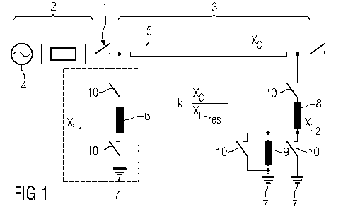
In order to provide a method for determining a switching time of an electric
switching device comprising an interrupter path (1) disposed between a first
line section
(2) subjected to a driving voltage (4) and a second line section (3) that
forms an
oscillating circuit after the switching device undergoes a shut-off step, said
method being
used for determining the best possible switching time for an electrical
switching device to
minimize transient voltage surges, it is proposed that either - a temporal
progression of a
voltage that develops along the interrupter path (1) is determined during a
scanning
period (t1), - the resonance frequency of the oscillation circuit is
determined from the
temporal progression, and a time window (.DELTA.t) is in turn determined from
the resonance
frequency, - and a switching time is established by determining a zero
crossover of an
envelope of a future progression after a defined time period (t2) following
the shut-off
process within the time window (.DELTA.t), said future progression being
calculated using the
temporal progression, said envelope corresponding to the resonance frequency;
or that - a
temporal progression of a voltage that develops along the interrupter path (1)
is
determined during a scanning time (t1), - a future progression of the voltage
along the
interrupter path and the resonance frequency of the oscillating circuit are
determined
from the temporal progression along with a time window (.DELTA.t) which in
turn is determined
from the resonance frequency, - and a switching time is established by
determining a zero
crossover of the voltage along the interrupter path after a defined time
period (t2) after
shutoff within the determined time window (.DELTA.t), said crossover being
weighted with
criteria of the driving voltage and oscillation circuit voltage.
L'invention concerne un procédé destiné à déterminer un moment de commutation d'un appareil de commutation électrique avec un segment de rupture (1) qui est disposé entre une première section de ligne (2) soumise à une tension de commande (4) et une deuxième section de ligne (3) formant un circuit oscillant après une opération de coupure de l'appareil de commutation, avec lequel on peut déterminer un moment de commutation le meilleur possible pour un appareil de commutation électrique afin de réduire les surtensions transitoires. Pour perfectionner ce procédé, il est proposé soit - de relever une courbe temporelle d'une tension survenant sur le segment de rupture (1) pendant une période de balayage (tl), de déterminer à partir de la courbe temporelle la fréquence de résonance du circuit oscillant et à partir de là, d'autre part, une fenêtre de temps (?t), - et de fixer dans la fenêtre de temps (?t) un moment de commutation par détermination d'un passage par zéro d'une enveloppante correspondant à la fréquence de résonance d'une courbe future calculée sur la base de la courbe temporelle après une période de temps définie (t2) après l'opération de coupure ; soit - de relever une courbe temporelle d'une tension survenant sur le segment de rupture (1) pendant une période de balayage (tl), - de déterminer à partir de la courbe temporelle relevée une courbe future d'une tension sur le segment de rupture, la fréquence de résonance du circuit oscillant et à partir de là, d'autre part, une fenêtre de temps (?t) - et de fixer dans la fenêtre de temps établie (?t) un moment de commutation par détermination d'un passage par zéro - pondéré avec des critères de la tension de commande et de la tension du circuit oscillant - de la tension sur le segment de rupture après une période de temps définie (t2) après l'opération de coupure.
Note: Claims are shown in the official language in which they were submitted.
Note: Descriptions are shown in the official language in which they were submitted.
2024-08-01:As part of the Next Generation Patents (NGP) transition, the Canadian Patents Database (CPD) now contains a more detailed Event History, which replicates the Event Log of our new back-office solution.
Please note that "Inactive:" events refers to events no longer in use in our new back-office solution.
For a clearer understanding of the status of the application/patent presented on this page, the site Disclaimer , as well as the definitions for Patent , Event History , Maintenance Fee and Payment History should be consulted.
| Description | Date |
|---|---|
| Application Not Reinstated by Deadline | 2016-05-12 |
| Time Limit for Reversal Expired | 2016-05-12 |
| Deemed Abandoned - Failure to Respond to Maintenance Fee Notice | 2015-05-12 |
| Change of Address or Method of Correspondence Request Received | 2015-01-15 |
| Letter Sent | 2014-03-24 |
| Request for Examination Received | 2014-03-17 |
| All Requirements for Examination Determined Compliant | 2014-03-17 |
| Request for Examination Requirements Determined Compliant | 2014-03-17 |
| Inactive: Cover page published | 2011-02-01 |
| Inactive: Notice - National entry - No RFE | 2011-01-06 |
| Inactive: First IPC assigned | 2011-01-05 |
| Inactive: IPC assigned | 2011-01-05 |
| Application Received - PCT | 2011-01-05 |
| National Entry Requirements Determined Compliant | 2010-11-12 |
| Application Published (Open to Public Inspection) | 2009-11-19 |
| Abandonment Date | Reason | Reinstatement Date |
|---|---|---|
| 2015-05-12 |
The last payment was received on 2014-04-07
Note : If the full payment has not been received on or before the date indicated, a further fee may be required which may be one of the following
Please refer to the CIPO Patent Fees web page to see all current fee amounts.
| Fee Type | Anniversary Year | Due Date | Paid Date |
|---|---|---|---|
| Basic national fee - standard | 2010-11-12 | ||
| MF (application, 2nd anniv.) - standard | 02 | 2011-05-12 | 2011-04-14 |
| MF (application, 3rd anniv.) - standard | 03 | 2012-05-14 | 2012-04-05 |
| MF (application, 4th anniv.) - standard | 04 | 2013-05-13 | 2013-04-09 |
| Request for examination - standard | 2014-03-17 | ||
| MF (application, 5th anniv.) - standard | 05 | 2014-05-12 | 2014-04-07 |
Note: Records showing the ownership history in alphabetical order.
| Current Owners on Record |
|---|
| SIEMENS AKTIENGESELLSCHAFT |
| Past Owners on Record |
|---|
| CHRISTIAN WALLNER |
| HANS-GEORG RICHTER |

