Note : Les descriptions sont présentées dans la langue officielle dans laquelle elles ont été soumises.
CA 02724224 2010-11-12
PCT/EP2009/055702 - 1 -
2008P08730WOUS
Description
Method for determining a switching time of an electrical
switching device
The invention relates to a method for determining a switching
time of an electrical switching device having an interrupter
gap which is arranged between a first line section, to which a
driving voltage is applied, and a second line section, which
forms a resonant circuit after a disconnection process of the
switching device.
By way of example, one such method is known from DE 10 2005 005
228 Al which discloses a method for determining a switching
time of an electrical switching device in the form of a
gas-insulated switch gear assembly, which connects a first line
section to a generator, which applies a driving voltage to the
first line section with a second line section in the form of an
overhead line, and can be disconnected therefrom. In a known
manner, an overhead line such as this forms a resonant circuit
after the electrical switching device has been disconnected and
has been isolated from the first line section with the
generator and the driving voltage, wherein, in a known manner,
the overhead line has both capacitive and inductive impedances
and can be compensated for by means of inductors as variable
inductances. When the first line section is connected to the
driving voltage, transient overvoltages occur, which can lead
to flashovers or other disturbances. Therefore, in order to
reduce these transient overvoltages, DE 10 2005 005 228 Al
discloses a method by means of which a switching time for
connection of an electrical switching device can be determined,
wherein mathematical
CA 02724224 2010-11-12
PCT/EP2009/055702 - 2 -
2008P08730WOUS
methods can be used to determine a switching time, which is
chosen to be as close as possible to zero crossings of the
driving voltage and of an oscillating voltage, which occurs in
the resonant circuit of the overhead line, by weighting with
different criteria. The method disclosed in DE 10 2005 005 228
Al for determining the time profiles of the voltages is in this
case based on the Prony method described there.
Another known method of the type mentioned initially is based
on so-called pattern recognition, in which a switching time of
an electrical switching device can be determined from a zero
crossing of an envelope of the voltage which occurs across the
interrupted path.
The method described in DE 10 2005 005 228 Al is complex
because, in this case, a multiplicity of successive zero
crossings of the driving voltage and of the resultant voltage
must be considered in relation to one another, and must be
weighted with different criteria. The other method, of pattern
recognition, does not always lead to the desired result,
because the envelope of the voltage which occurs across the
interrupter gap is at a frequency which is dependent on the
compensation level of the overhead line and therefore on the
resonant frequency of the resonant circuit, as a result of
which, in the case of a fixed time window, there may be no such
zero crossing of the envelope for a changed compensation level
in the time window, and it is therefore not possible to
determine the best possible switching time.
The object of the present invention is to design a method of
the type mentioned initially which makes it possible to
determine the best possible switching time for an electrical
switching device, in order to minimize transient overvoltages.
CA 02724224 2010-11-12
PCT/EP2009/055702 - 3 -
2008P08730WOUS
According to the invention, this object is achieved in the case
of a method of the type mentioned initially in that:
- a time profile of a voltage which occurs across the
interrupter gap is determined during a sampling time period,
- the resonant frequency of the resonant circuit and, from
this in turn, a time window are determined from the time
profile,
- and a switching time is defined in the time window by
determining a zero crossing of an envelope, which corresponds
to the resonant frequency, of a future profile, calculated on
the basis of the time profile, after a defined time period
after the disconnection process.
In this case, the method according to the invention has the
advantage that the determined time window is determined by the
resonant frequency of the resonant circuit which is formed by
the overhead line with its capacitive line impedance and the
compensation inductors, as a function of the compensation
level, thus ensuring that this time window will contain a zero
crossing of the envelope of the time profile of the voltage
which occurs across the interrupter gap, and an optimum
switching time can therefore be determined in the time window,
and the switching device and the first line section can be
connected to the second line section with the lowest possible
transient overvoltages. The defined time period after the
disconnection process is in this case determined from general
requirements for the switching time, for example, in the case
of a high-voltage transmission line this may be a time period
of 300 ms, after which, for example, the switching device may
be connected again, at the earliest, in the event of a brief
interruption.
CA 02724224 2010-11-12
PCT/EP2009/055702 - 4 -
2008P08730WOUS
In another refinement of the method according to the invention,
the stated object is achieved in that:
- a time profile of a voltage which occurs across the
interrupter gap is determined during a sampling time period,
- a future profile of the voltage across the interrupter
gap, the resonant frequency of the resonant circuit and, from
this in turn, a time window are determined from the determined
time profile,
- and a switching time is defined in the determined time
window by determining a zero crossing, which is weighted with
criteria of the driving voltage and of the resonant circuit
voltage, of the voltage across the interrupter gap after a
defined time period after the disconnection process.
The one zero crossing of the voltage, which is weighted with
criteria of the driving voltage and resonant circuit voltage,
across the interrupter gap is in this case as described in DE
2005 005 228 Al which, with this reference, is part of the
present disclosure. Advantageously in this case, in the case of
the method according to the invention, the number of profile
points to be related to one another in the driving voltage and
resonant circuit voltage for zero crossings of the determined
voltage across the interrupter gap, and their weighting with
respect to one another is limited to the time period determined
by the time window, thus considerably reducing the complexity
that has to be accepted, because the determined time window is
determined by the resonant frequency of the resonant circuit
which is formed by the overhead line with its capacitive line
impedance and the compensation inductors, as a function of the
compensation level, thus ensuring that, in this time window, an
optimum switching time can be determined in the time window
CA 02724224 2010-11-12
PCT/EP2009/055702 - 5 -
2008P08730WOUS
and the switching device and the first line section can be
connected to the second line section with the lowest possible
transient overvoltages. The defined time period after the
disconnection process is in this case determined from general
requirements for the switching time, for example in the case of
a high-voltage transmission line this may be a time period of
300 ms, after which, for example, the switching device may be
switched on again in the event of a brief interruption.
The invention will be explained in more detail in the following
text using the figure and exemplary embodiments, and with
reference to the attached figures, in which:
Figure 1 shows a schematic layout of an electrical power
transmission system,
Figure 2 shows the profile of a resultant voltage, and
Figure 3 shows a profile of various voltages.
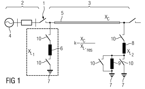
Figure 1 shows a basic layout of a line section within an
electrical power transmission system. An electrical switching
device has an interrupter gap 1 which, for example, is formed
from two contact pieces which can move relative to one another.
A first line section 2 and a second line section 3 can be
connected to one another and disconnected from one another via
the interrupter gap 1. The first line section 2 has a generator
4 which produces a driving voltage which, for example, is a 50
Hz AC voltage of a polyphase voltage
CA 02724224 2010-11-12
PCT/EP2009/055702 - 6 -
2008P08730WOUS
system. The second line section 3 has an overhead line 5 which
can be connected at its first end to a first inductor 6, with
respect to ground potential 7, and at its second end via a
second inductor 8 to ground potential 7. Furthermore, it is
additionally possible for a further inductor 9 to be connected
to the second inductor 8. The inductors 6, 8, 9 can be
connected in various variants to the ground potential 7 by
means of different switching devices 10. It is thus possible to
compensate the overhead line 5 to different extents as a
function of the load situation, as a result of which the
capacitive impedance XC of the overhead line can be
overcompensated or undercompensated by means of the inductive
impedance XL. A compensation level K can be determined by the
ratio of the capacitive impedance XC of the overhead line and
the inductive impedance XL of all the inductors. The inductors
6, 8, 9 can be switched differently with respect to one another
in order to adjust the compensation level K. However, it is
also possible for the inductors to have a variable inductive
impedance XL. Plunger-type core inductors can be used, for
example, for this purpose.
After the interrupter gap 1 has been opened, a resonant circuit
can be formed via the ground potential 7 in the second line
section 3. In order to form a resonant circuit in the second
line section 3, appropriate current paths must be formed via
the switching devices 10 to the ground potential 7. A resonant
circuit is formed via the inductive and capacitive impedances,
and an oscillating current can flow in the resonant circuit,
driven by an oscillating voltage.
By way of example, Figure 2 shows a resultant voltage profile
which is formed across the interrupter gap 1 for
CA 02724224 2010-11-12
PCT/EP2009/055702 - 7 -
2008P08730WOUS
a specific compensation level by the inductors 6, 8 and 9. The
voltage profile has a multiplicity of voltage zero crossings
and exhibits a beat, which is essentially governed by the
compensation level of the overhead line and therefore by the
resonant frequency of the resonant circuit of the overhead
line. After a disconnection process of the switching device 1
of the time t = 0, the resultant voltage signal is now sampled
during a sampling time period t1, which is greater than, less
than or else equal to a time which corresponds to the resonant
frequency, and an envelope, which is illustrated by dashed
lines, and therefore the resonant frequency of the resonant
circuit and the compensation level of the overhead line, are
determined from this, in order in turn to determine a time
window At from this, within which there must be a zero crossing
of the envelope of the voltage signal, because its width
corresponds to at least one half-cycle of the period of the
envelope of the voltage signal. After a disconnection process
of the switching device 1, the switching device 1 can once
again be connected after a specific time period t2, as the
earliest possible connection time, depending on the requirement
of the electrical power transmission system, wherein the time
frame of the window width At for the connection of the
switching device 1 is available from the time t2, in which time
frame At there is at least one zero crossing of the envelope of
the voltage signal, at which time the switching device can then
be connected with the lowest possible transient overvoltages.
Figure 3 shows another possible way to determine an optimum
switching time for the switching device 1. Al in this case
shows the time profile of the driving voltage for the generator
4 in Figure 1, Bl shows the time profile of the resultant
oscillating voltage on the overhead line 5 of the second
CA 02724224 2010-11-12
PCT/EP2009/055702 - 8 -
2008P08730W0US
line section 3 from Figure 1, and Cl shows the resultant
voltage across the interrupter unit 1, as the difference
between the driving voltage Al and the oscillating voltage B1.
The zero crossings of the resultant voltage Cl represent
potential switching times, in which case optimum switching
times for connection of a switching device can also be found by
weighting, by means of the profiles of the driving voltage Al
and the oscillating voltage B1, as already described in DE 10
2005 005 228 Al, which is hereby part of the present
disclosure. In this case, in the exemplary embodiment, the
voltage profile is determined during a time period t1 after
disconnection of the switching device and a time window is
determined from this, as already described with reference to
Figure 2, on the basis of the resonant frequency of the
resonant circuit and therefore the compensation level of the
overhead line, such that, after an earliest possible time
period t2, which is governed by the requirements of the
electrical power transmission system, the time window At which
results from the resonant frequency of the resonant circuit is
available for a switching time, in which time window At zero
crossings of the resultant voltage Cl are determined at the
times Tl and T2 as possible switching times, with the profiles
of the driving voltage Al and of the oscillating voltage Bl
being weighted by mathematical methods as described in DE 10
2005 005 228 Al. For this purpose, the voltage profiles Al, B1
and Cl are considered and related to one another only in the
time window At.