Note: Descriptions are shown in the official language in which they were submitted.
CA 02724528 2016-05-09
TELECOMMUNICATIONS WIRE HAVING A CHANNELED DIELECTRIC
INSULATOR AND METHODS FOR MANUFACTURING THE SAME
Technical Field
The present disclosure relates generally to twisted pair telecommunication
wires for use in telecommunication systems. More specifically, the present
disclosure
relates to twisted pair telecommunications wires having channeled dielectric
insulators.
Background
Twisted pair cables are commonly used in the telecommunications industry to
transmit data or other types of telecommunications signals. A typical twisted
pair
cable includes a plurality of twisted wire pairs enclosed within an outer
jacket. Each
twisted wire pair includes wires that are twisted together at a predetermined
lay
length. Each wire includes an electrical conductor made of a material such as
copper,
and a dielectric insulator surrounding the electrical conductor.
The telecommunication industry is driven to provide telecommunication cables
capable of accommodating wider ranges of signal frequencies and increased
bandwidth. To improve performance in a twisted wire pair, it is desirable to
lower the
dielectric constant (DK) of the insulator surrounding each electrical
conductor of the
twisted pair. As disclosed in US Patent No. 7,049,519, the insulators of the
twisted
pairs can be provided with air channels. Because air has a DK value of 1, the
air
channels lower the effective DK value of the insulators thereby providing
improved
performance.
Providing an insulator with increased air content lowers the effective DK
value
of the insulator. However, the addition of too much air to the insulator can
cause the
insulator to have poor mechanical/physical properties. For example, if too
much air is
present in an insulator, the insulator may be prone to crushing. Thus,
effective twisted
pair cable design involves a constant balance between insulator DK value and
insulator physical properties.
1
CA 02724528 2016-05-09
Summary
One aspect of the present disclosure relates to a telecommunication wire
having a dielectric insulator that exhibits a low dielectric constant in
combination with
demonstrating desirable mechanical properties such as enhanced crush
resistance
and suitable fire prevention characteristics. Another aspect of the present
disclosure
relates to a method for manufacturing a telecommunication wire having a
dielectric
insulator as described above.
Examples representative of a variety of aspects are set forth in the
description
that follows. The aspects relate to individual features as well as
combinations of
features. It is to be understood that both the forgoing general description
and the
following detailed description merely provide examples of how the aspects may
be
put to into practice, and are not intended to limit the broad spirit and scope
of the
aspects.
In accordance with one aspect of the invention, there is provided a
telecommunications wire comprising:
an electrical conductor; and
a dielectric insulator surrounding the electrical conductor, the dielectric
insulator defining a plurality of closed channels and a plurality of open
channels, the
closed channels and the open channels defining void space containing a gaseous
material, the closed and the open channels being circumferentially spaced
about the
electrical conductor, the closed channels and the open channels each running
generally along a length of the electrical conductor, and the closed channels
defining
at least 75 percent of the void space, wherein the dielectric insulator
includes an outer
circumferential wall defining an outer diameter of the dielectric insulator,
an inner
circumferential wall spaced radially inwardly from the outer circumferential
wall, and a
plurality of radial walls that extend between the inner and outer
circumferential walls,
wherein the closed channels are defined between the inner and outer
circumferential
walls, and wherein the inner circumferential wall, the outer circumferential
wall and
the radial walls each have a thickness in the range of .001 to .0035 inches.
Another aspect of the invention provides a telecommunications wire
comprising:
2
CA 02724528 2016-05-09
an electrical conductor; and
a dielectric insulator surrounding the electrical conductor, the dielectric
insulator defining a plurality of closed channels and a plurality of open
channels, the
closed channels and the open channels defining void space containing a gaseous
material, the closed and the open channels being circumferentially spaced
about the
electrical conductor, the closed channels and the open channels each running
generally along a length of the electrical conductor, and at least one of the
closed
channels defining a transverse cross-sectional area that is at least two times
larger
than a transverse cross-sectional area defined by at least one of the open
channels,
wherein the dielectric insulator includes an outer circumferential wall
defining an outer
diameter of the dielectric insulator, an inner circumferential wall spaced
radially
inwardly from the outer circumferential wall, and a plurality of radial walls
that extend
between the inner and outer circumferential walls, wherein the closed channels
are
defined between the inner and outer circumferential walls, and wherein the
inner
circumferential wall, the outer circumferential wall and the radial walls each
have a
thickness in the range of .001 to .0035 inches.
Still another aspect of the invention provides a telecommunications wire
comprising:
an electrical conductor; and
a dielectric insulator surrounding the electrical conductor, the dielectric
insulator including an outer circumferential wall defining an outer diameter
of the
dielectric insulator, an inner circumferential wall spaced radially inwardly
from the
outer circumferential wall, and a plurality of radial walls that extend
between the inner
and outer circumferential walls, the dielectric insulator also defining more
than 12
closed channels between the inner and outer circumferential walls, the outer
diameter
of the dielectric insulator being less than .05 inches;
the dielectric insulator defining a percentage void area in the range of 15-25
percent;
the inner circumferential wall, the outer circumferential wall and the radial
walls
each having a thickness in the range of .001 to .0035 inches;
2a
CA 02724528 2016-05-09
the dielectric insulator having a minimum material thickness in the range of
.002-.007 inches; and
the dielectric insulator has a maximum material thickness in the range of 1.5-
3.0 times as thick as the minimum material thickness of the dielectric
insulator,
wherein the dielectric insulator also defines open channels having open sides
that face toward the electrical conductor, and wherein the closed cells define
at least
75 percent of the void area of the dielectric insulator.
Brief Description of the Drawings
Aspects of the disclosure may be more completely understood in consideration
of the following detailed description of various embodiments of the disclosure
in
connection with the accompanying drawings, in which:
Figure 1 is a transverse, cross-sectional view of a telecommunication wire
having a conductor disposed through a central passageway of a dielectric
insulator;
Figure 2 is perspective view of two of the telecommunication wires of Figure 1
incorporated into a twisted wire pair;
Figure 3 is a view of a longer segment of the twisted wire pair of Figure 2;
Figure 4 is a transverse, cross-sectional view of a telecommunication cable
having a core that includes four twisted wire pairs of the type shown in
Figure 2;
Figure 5 is a transverse, cross-sectional view of an alternate embodiment of a
telecommunication wire;
Figure 6 is a transverse, cross-sectional view of a telecommunication cable
having a core that includes four twisted wire pairs of the type shown in
Figure 5;
2b
CA 02724528 2010-11-15
WO 2010/002720
PCT/US2009/048770
Figure 7 is a transverse, cross-sectional view of an additional alternate
embodiment of a telecommunication wire;
Figure 8 is a transverse, cross-sectional view of a telecommunication cable
having a core that includes four twisted wire pairs of the type shown in
Figure 7;
Figure 9 illustrates a system for manufacturing telecommunication cables in
accordance with the principles of the present disclosure;
Figure 10 is a cross-sectional view of an example crosshead tip and die that
can be used with the system of Figure 9;
Figure 11 is a perspective of the example crosshead tip and die of Figure 10;
Figure 12 is a perspective view of an example crosshead tip and die of Figure
11 having a collar removed from the die;
Figure 13 is an end view of the crosshead of Figure 11;
Figure 14 shows a crosshead tip and die with a pressurization manifold;
Figure 15 shows an alterative tip in accordance with the principles of the
present disclosure; and
Figure 16 shows another crosshead die with a pressurization manifold.
Detailed Description
The present disclosure relates generally to twisted pair telecommunication
wires for use in telecommunication systems. More specifically, the present
disclosure relates to twisted pair telecommunications wires having channeled
dielectric insulators. Dielectric insulators in accordance with the principles
of the
disclosure exhibit a reduced dielectric constant in combination with
demonstrating
desirable mechanical properties such as enhanced crush resistance and suitable
fire
prevention characteristics.
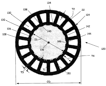
Figure 1 is a transverse, cross-sectional view of a telecommunication wire
120 having features in accordance with the principles of the present
disclosure. The
telecommunication wire 120 includes an electrical conductor 22 surrounded by a
dielectric insulator 124. The dielectric insulator 124 includes an inner
circumferential wall 126 and an outer circumferential wall 128. The outer
circumferential wall 128 is spaced radially outwardly from the inner
circumferential
wall 126. A plurality of radial walls 130 (e.g., spokes) extend from the inner
circumferential wall 126 to the outer circumferential wall 128. A plurality of
closed
channels 132 (e.g., 18 closed channels) are defined within the dielectric
insulator
3
CA 02724528 2010-11-15
WO 2010/002720
PCT/US2009/048770
124. For example, the closed channels 132 are shown defined between the inner
and
outer circumferential walls 126, 128 with the channels 132 being separated
from one
another by the radial walls 130. A closed channel is a channel that is fully
surrounded by or enclosed within portions of the dielectric insulator. The
closed
channels 132 are preferably filled with a gaseous dielectric material such as
air.
The dielectric insulator 124 also includes a plurality of projections or legs
134 that project radially inwardly from the inner circumferential wall 126
toward a
center axis 136 of the dielectric insulator 124. The legs 134 have base ends
138 that
are integrally formed with an inner side of the inner circumferential wall
126, and
free ends 140 that are spaced radially inwardly from the base ends 138. The
free
ends 140 define an inner diameter (ID) of the dielectric insulator 124. As
shown at
Figure 1, the free ends 140 are adapted to engage the outer diameter of the
electrical
conductor 22. The outer circumferential wall 128 defines an outer diameter
(OD) of
the dielectric insulator 124.
A plurality of open channels 142 are defined between the legs 134. The open
channels 142 of the dielectric insulator 124 are each shown having a
transverse
cross-section that is notched shaped with open sides/ends 144 located at the
inner
circumferential wall 126. The open sides/ends 146 face radially toward the
center
axis 136. The dielectric insulator 124 defines an interior passage 150 having
a
central region in which the electrical conductor 22 is located, and peripheral
regions
defined by the open channels 142.
As shown at Figure 1, each of the open channels 142 is radially aligned with
a corresponding one of the closed channels 132. Thus, one of the open channels
142
is provided for each of the closed channels 132. Moreover, it is preferred for
the
closed channels 132 to be substantially larger in cross-sectional area than
the open
channels 142. For example, in one embodiment, each of the closed channels 132
is
at least two times as large as the cross-sectional area of the corresponding
open
channel 142. In other embodiments, each of the closed channels 132 has a cross-
sectional area that is at least five times as large as the cross-sectional
area of its
corresponding open channel 142. In still another embodiment, each of the
closed
channels 132 has a cross-sectional area that is at least ten or twenty times
as large as
the area of the corresponding open channel 142.
It is preferred for the inner cylindrical wall 126; the outer cylindrical wall
128 and the radial walls 130 to all have approximately the same thickness to
4
CA 02724528 2010-11-15
WO 2010/002720
PCT/US2009/048770
facilitate the extrusion process. In calculating the thickness of the inner
cylindrical
wall 126, the radial lengths of the legs 134 are considered as part of the
thickness of
the inner circumferential wall 126.
The channels 132, 142 are preferably filled with a material having a low
dielectric constant (e.g., a gaseous material such as air). Since air has a
dielectric
constant of one, to minimize the overall dielectric constant of the dielectric
insulator
124, it is desirable to maximize the percent void area within the dielectric
insulator
124 that contains air. The percent void area is calculated by dividing the
void area
defined by a transverse cross-section of the dielectric insulator (i.e., the
total
transverse cross-sectional area defined by the channels) by the total
transverse cross-
sectional area defined between the inner and outer diameters of the dielectric
insulator.
Referring to Figure 1, the inner circumferential wall 126 has a wall thickness
T1, the outer circumferential wall 128 has a wall thickness T2 and the radial
walls
130 have wall thicknesses T3. In one embodiment, the wall thicknesses T1, T2
and
T3 can each be in the range of .0015-.0025 inches or preferably about .002
inches,
the outer diameter of the dielectric insulator 124 can be in the range of .041-
.046 or
preferably about .0435 inches, the inner diameter of the dielectric insulator
can be
about .021-.025 inches or preferably about .023 inches, the minimum material
thickness of the dielectric insulator can be in the range of .003-.005 or
preferably
about .004 inches, the maximum material thickness can be in the range of .008-
.012
inches or about .01025 inches, and the percent void area defined by the
dielectric
insulator 124 can be in the range of 30-50 percent or about 41 percent. In one
embodiment, 8-25 of the closed channels preferably define at least 75 percent
of the
void area and more preferably define at least 90 percent of the void area. In
another
embodiment, 13-18 of the closed channels preferably define at least 75 percent
of
the void area and more preferably define at least 90 percent of the void area.
Figures 2-3 show two of the telecommunication wires 120 incorporated into
a twisted wire pair 160. As shown in Figure 3, the telecommunication wires 120
are
twisted about one another at a predetermined lay length Li. It will be
appreciated
that the lay length can be generally constant, can be varied in a controlled
manner,
and can also be randomly varied. For the crush resistance properties provided
by the
dielectric insulators 124 of the wires 120, it is desirable for the lay length
of the
twisted pairs to be in the range of .5-.9 inches, or greater than .5 inches.
5
CA 02724528 2010-11-15
WO 2010/002720
PCT/US2009/048770
Figure 4 shows four of the twisted wire pairs 160 of Figures 2-3 incorporated
into a four-pair telecommunications cable 170. Outer circles 150 are
representative
of the outer boundaries defined by the telecommunication wires 120 as the
telecommunication wires are twisted around one another to form the twisted
wire
pairs 160. Four twisted wire pairs 160 are separated by a filler 80 positioned
at a
central location of the cable 170. In one embodiment, the filler 80 is
manufactured
of a polymeric dielectric insulator material such as foamed FEP. It will be
appreciated that the filler 80 and the four twisted wire pairs 160 define a
cable core
that is twisted about a center axis of the cable 170 at a predetermined lay
length. It
will be appreciated that the core lay length can be randomly varied,
maintained at a
constant length, or varied in a controlled, but non-random manner. An outer
jacket
190 covers the cable core.
Figure 5 shows a further telecommunication wire 220 in accordance with the
principles of the present disclosure. The telecommunication wire 220 has the
same
configuration as the wire 120 of Figure 1 except an inner circumferential wall
226,
an outer circumferential wall 228 and radial walls 230 have an increased
thickness to
improve crush resistance. For example, in one embodiment, the inner
circumferential wall 226, the outer circumferential wall 228 and the radial
walls 230
each have a wall thickness in the range of .002 to .003. Such an embodiment
can
have a dielectric insulator with an outer diameter of about .041-.046 inches
or
preferably about .0437 inches, an inner diameter of about .021-.025 or
preferably
about .0230 inches, a percent void area in the range of 25-35 percent or
preferably
about 30 percent, a minimum material thickness of about .004-.006 inches or
preferably about .0045 inches and a maximum material thickness in the range of
in
the range of .008-.012 inches or preferably about .01025 inches. In one
embodiment, 8-25 of the closed channels preferably define at least 75 percent
of the
void area and more preferably define at least 90 percent of the void area. In
another
embodiment, 13-18 of the closed channels preferably define at least 75 percent
of
the void area and more preferably define at least 90 percent of the void area.
Figure 6 shows a plurality of the telecommunication wires 220 twisted into
twisted pairs and incorporated into a telecommunications cable of a type
described
with respect to Figure 4. For the crush resistance properties provided by the
dielectric insulators of the wires 220, it is desirable for the lay length of
each of the
twisted pairs to be in the range of .4-.9 inches, or greater than .4 inches.
6
CA 02724528 2010-11-15
WO 2010/002720
PCT/US2009/048770
Figure 7 shows a further telecommunication wire 320 in accordance with the
principles of the present disclosure. The telecommunication wire 320 has the
same
configuration as the telecommunication wire 120, except inner circumferential
wall
326, outer circumferential wall 328 and radial walls 330 of dielectric
insulator 324
are thicker to provide enhanced crush resistance. Further, the wire 320 only
has
sixteen radial walls as compared to eighteen as shown in the embodiment of
Figure
1. Thus, the telecommunication wire 320 has sixteen closed channels 332 and
eighteen open channels 342. It is preferred for the walls 324, 326 and 328 to
each
have a thickness T in the range of .0027 inches to .0033 inches. In a
preferred
embodiment, the thicknesses T are about .003 inches. In the depicted
embodiment,
the dielectric insulator 324 has an outer diameter in the range of .041-.046
inches or
preferably about .0437 inches, an inner diameter in the range of .021-.025 or
preferably about .0230 inches, a percent void area in the range of 15% to 25%,
a
minimum material thickness in the range of .045-.065 or preferably about .0055
inches, and a maximum material thickness of about .008-.012 inches or
preferably
about .01025 inches. Additionally, the dielectric insulator 324 includes a
different
number of open channels 342 as compared to closed channels 332. For example,
the
dielectric insulator 324 can include more or fewer open channels 342 as
compared to
closed channels 332. Additionally, in the dielectric insulator 324, the open
channels
342 do not radially align with the closed channels 332. In one embodiment, 13-
16
of the closed channels preferably define at least 75 percent of the void area
and more
preferably define at least 90 percent of the void area.
Figure 8 shows a plurality of the wires 320 twisted into four sets of twisted
pairs and incorporated into a telecommunications cable of the type described
with
respect to Figure 4. For the crush resistance properties provided by the
dielectric
insulators of the wires 320, it is desirable for the lay length of each of the
twisted
pairs to be in the range of .2-.9 inches or .3-.8 inches. Due to improved
crush
resistance, the wires 320 can be paired at lay lengths less than .4 inches or
less than
.35 inches without experiencing problems related to crushing.
To provide acceptable levels of crush resistance while maximizing the
amount of void provided within the dielectric insulator, certain embodiments
of the
present disclosure have dielectric insulators with more than 8 closed
channels, or at
least 12 closed channels, or at least 16 closed channels, or at least 18
closed
channels. Further embodiments have dielectric insulators with more than 6 open
7
CA 02724528 2010-11-15
WO 2010/002720
PCT/US2009/048770
channels or more than 12 open channels, or at least 16 open channels or at
least 18
open channels. Still other embodiments have more than 6 open channels and more
than 6 closed channels, or more than 12 open channels and more than 12 closed
channels, or at least 16 open channels and at least 16 closed channels, or at
least 18
open channels and at least 18 closed channels. In certain embodiments, only
closed
channels may be provided or only open channels may be provided.
To provide acceptable levels of crush resistance while also providing the
dielectric insulator with a suitably low dielectric constant, it is desirable
to carefully
select the percent void area of a given dielectric insulator in accordance
with the
principles of the present disclosure. Certain embodiments have dielectric
insulators
with percent void areas in the range of 5-50%, or 15-45%, or 15-40%, or 15-
35%, or
15-30%, or 15-25%, or 20-45%, or 20-40%, or 20-35%, or 20-30%, or 20-25%, or
18-23%.
It will be appreciated that dielectric insulators in accordance with the
principles of the present disclosure can be made of any number of types of
materials
such as a solid polymeric material or a foamed polymeric material. In one
embodiment, the walls of the insulator can be formed of solid fluorinated
ethylene-
propylene (FEP) or foamed FEP. While FEP or MFA are preferred materials for
manufacturing the walls of the dielectric insulator, it will be appreciated
that other
materials can also be used. For example, other polymeric materials such as
other
fluoropolymers can be used. Still other polymeric materials that can be used
include
polyolefins, such as polyethylene and polypropylene based materials. In
certain
embodiments, high density polyethylene may also be used.
Dielectric insulators in accordance with the principles of the disclosure
preferably have a relatively low dielectric constant in combination with
exhibiting
desirable mechanical properties such as enhanced crush resistance and suitable
fire
prevention characteristics. For example, telecommunications wire in accordance
with the principles of the present disclosure can be manufactured so as to
comply
with National Fire Prevention Association (NFPA) standards for how material
used
in residential and commercial buildings burn. Example standards set by the
NFPA
include fire safety codes such as NFPA 255, 259 and 262. The UL 910 Steiner
Tunnel burn test serves the basis for the NFPA 255 and 262 standards.
Telecommunication wires in accordance with the principles of the present
disclosure
can have various sizes.
8
CA 02724528 2010-11-15
WO 2010/002720
PCT/US2009/048770
In certain embodiments, telecommunication wires in accordance with the
principles of the present disclosure can have dielectric insulators with an
outer
diameter OD in the range of .03 to .05 inches or in the range of .04 to .045
inches or
less than about .060 inches or less than about .070 inches. The inner
diameters of
dielectric insulators in accordance with the principles of the present
disclosure
generally correspond to the outer diameters of the electrical conductors
covered by
the dielectric insulators. In certain embodiments, the inner diameters of the
dielectric insulators range from .015 to .030 inches or in the range of .018-
.027
inches, or in the range of .020-.025 inches, or less than .030 inches.
Electrical conductors in accordance with the principles of the present
disclosure preferably are manufactured out of an electrically conductive
material
such as a metal material such as copper or other materials. It will be
appreciated that
the electrical conductors in accordance with the principles of the present
disclosure
can have a solid configuration, a stranded configuration or other
configurations such
as aluminum coated with a copper or tin alloy.
The channels (e.g., closed or open) of dielectric insulators in accordance
with
the principles of the present disclosure preferably have lengths that run
generally
along a length of the electrical conductor. For certain twinning and back
twisting
operations used to manufacture twisted pair cable, twists can be applied to
each of
the telecommunication wires of a twisted pair. In this situation, the channels
can
extend in a helical pattern around the electrical conductor as the channels
run
generally along the length of the electrical conductor.
In certain embodiments, the wall thicknesses T1, T2 and T3 the walls of
dielectric insulators in accordance with the present disclosure (e.g., inner
and outer
circumferential walls and radial walls) can each have a thickness ranging from
.0015-.005 inches, or .002-.004 inches, or .002-.0035 inches, or .0025-.004
inches,
.0025-.0035 inches, or .0025-.004 inches, or .003-.004 inches, or .003-.0035
inches,
or .0027-.0033 inches. It will be appreciated that the thicknesses of the
walls are
selected to provide desired levels of crush resistance and desired levels of
void space
within the dielectric insulator.
To reduce cost, it is desirable to use the minimum amount of material needed
to provide adequate levels of crush resistance and relatively low dielectric
constant
values. In certain embodiments, the minimum material thickness of a dielectric
insulator in accordance with the principles of the present disclosure is less
than .01
9
CA 02724528 2010-11-15
WO 2010/002720
PCT/US2009/048770
inches, or less than .007 inches, or less than .0065 inches or less than .006
inches. In
other embodiments, the minimum material thickness of a dielectric insulator in
accordance with the principles of the present disclosure is in the range of
.003-.007
inches, or .0035-.007 inches, or .004-.007 inches, or .0045-.007 inches, or
.005-.007
inches. The minimum material thickness of a dielectric insulator is equal to
the
minimum total radial thickness of material defined between the outer diameter
of the
dielectric insulator and the outer diameter of the electrical conductor. In
the case of
the embodiment of Figure 1, the minimum material thickness equals the
thickness T1
of the inner circumferential wall 26 combined with the thickness T2 of the
outer
circumferential wall 28. This value equals the total thickness of the
dielectric
insulator (i.e., the thickness defined between the inner and outer diameters
of the
dielectric insulator) minus the radial thickness T4 of the channels 32. The
maximum
material thickness of a dielectric insulator is equal to the maximum total
radial
thickness of material defined between the outer diameter of the dielectric
insulator
and the outer diameter of the electrical conductor. In the case of the
embodiment of
Figure 1, the maximum material thickness is measured radially through one of
the
spokes and extends the full radial distance between the outer diameter of the
dielectric insulator and the outer diameter of the electrical conductor. In
certain
embodiments, dielectric insulators in accordance with the principles of the
present
disclosure have a maximum material thickness in the range of 1.5-6, or 1.5-5,
or 1.5-
4.0, or 1.5-3.5, or 1.5-3.0, or 1.5-2.5 times as thick as a minimum material
thickness.
Referring now to Figure 9, an example system 400 for use in extruding a
dielectric insulator over an electrical conductor 401 is shown. Generally, the
system
400 includes a crosshead 405 supporting a tip 450 positioned within a die 455.
The
system 400 also includes an extruder 425 for forcing a flowable dielectric
material
(e.g., a thermoplastic material) through the crosshead 405 to form the
dielectric
insulator about the electrical conductor 401. The extruder 425 can receive the
dielectric material from a hopper 420. The extruder 425 can also interface
with a
heating device 430 that heats the dielectric material to a desired temperature
suitable
for mixing, flowability and extrusion. The system 400 further includes a spool
440
for feeding the electrical conductor 401 to the crosshead 405, a vacuum source
480
for facilitating drawing down the dielectric material onto the electrical
conductor
401 after extrusion, a cooling bath 480 for cooling the dielectric insulator
after draw
CA 02724528 2010-11-15
WO 2010/002720
PCT/US2009/048770
down, and a take-up spool 485 for collecting the wire product after the
manufacturing process has been completed.
In use of the system 400, dielectric material 410 is conveyed from the hopper
420 to the crosshead 405 by the extruder 425. Within the extruder, the
dielectric
material is heated, masticated and pressurized. Pressure from the extruder 425
forces the flowable dielectric material through an annular passageway defined
between the tip 450 and the die 455 supported by the crosshead 405. As the
thermoplastic material is extruded through the annular passageway between the
tip
450 and the die 455, the electrical conductor 401 is fed from the spool 440
and
passed through an inner passageway 445 defined by the tip 450. As the
dielectric
material is passed between the tip 450 and the die 455, a desired transverse
cross-
sectional shape is imparted to the dielectric material. After the dielectric
material
has been extruded, the shaped dielectric material is drawn-down upon the
electrical
conductor 401 with the assistance of vacuum provided by the vacuum source 480
that controls the pressure within the central passage of the extruded
dielectric
material or with the assistance of pressurized air from a source of compressed
air.
After the dielectric material has been drawn-down upon the electrical
conductor 401,
the electrical conductor 401 and the dielectric material are passed through
the
cooling bath 480 to cool the dielectric material and set a final cross-
sectional shape
of the dielectric material. Thereafter, the completed telecommunications wire
435 is
collected on the take-up spool 485.
Figures 10-12 show a tip and die configuration 405' that can be incorporated
into the system of Figure 9 and used to manufacture the telecommunications
wire
320 of Fig. 7. The tip and die configuration 405' includes a die 455' and a
tip 450'
between which an annular extrusion passage 460' is defined. The die 455' is
shown
including a plurality of axial channel forming members 470' positioned within
the
annular extrusion passage 460'. The axial channel forming members 470' are
configured to form the closed channels 332 of the dielectric insulator 324
when
thermal plastic material flows through the extrusion passage 460' and around
the
channel forming members 470'. Each of the respective axial channel forming
members 470' includes an air passage 475' to provide air into the closed
channels
332 during the extrusion process via one or more holes 480' defined through
the die
455'. For example, an air manifold 490' (shown at Fig. 14) can be used to
direct
pressurized air from a source of compressed air into the holes 480' and
through the
11
CA 02724528 2010-11-15
WO 2010/002720
PCT/US2009/048770
air passages 475'. Alternatively, air at atmospheric pressure can be drawn
into the
air passages 475' through the holes 480' during the extrusion process. In
other
embodiments, different types of gaseous material may supplied to the closed
channels 332 during extrusion. For example, in another embodiment, an inert
gas
such as argon could be used.
Referring still to Figures 10-12, the tip 450' includes structure for forming
the open channels 342 of the dielectric insulator 324 during the extrusion
process.
For example, the tip 450' defines a plurality of channel forming members 465'
that
project radially outwardly from a main body of the tip 450' and into the
extrusion
passage 460'. During the extrusion process, the dielectric material being
extruded
through the extrusion passage 460' flows around the channel forming members
465'
such that the open channels 342 are formed during the extrusion process. A
collar/insert in the form of a truncated cone 485' (see Figure 10) or other
type of
tapered structure can be used to funnel the dielectric material into the
passage
between the tip 450' and the die 455' to ensure that the material flows
uniformly
throughout the entire open area (i.e., the area not occupied by members 470'
or
members 465' of the passage 460').
Referring to Figure 13, the tip and die configuration 405' includes a first
gap
G1 for forming the inner circumferential wall 126, a second gap G2 for forming
the
outer circumferential wall 128 and gaps G3 for forming the radial walls 130
have
wall thicknesses T3. To facilitate extruding the dielectric insulator 324, it
is
desirable for the gaps to be approximately the same size. For example, in one
embodiment, the gap sizes do not vary from one another by more than about 10%
or
5%.
For certain applications, it is preferred for a draw-down ratio of at least 50
to
1, or at least 100 to 1, or at least 150 to 1 to be used when extruding
dielectric
insulators of the type described above. A draw-down ratio is defined as the
cross-
sectional area of the extruded dielectric formed in the tooling divided by the
cross-
sectional area of material on the insulated conductor after the drawing
process has
been completed.
Fig. 15 shows an alternative tip arrangement 550 where axial channel
defining members 570 for forming the closed channels 332 and projections 565
for
forming the open channels 342 are provided on the tip.
12
CA 02724528 2010-11-15
WO 2010/002720
PCT/US2009/048770
Fig. 16 shows a modified compression manifold 590 for providing air to the
holes 480' and through the air passages 475' of the axial channel defining
members
470' of the die 455'. The manifold 590 includes a first flow path 591 in fluid
communication with a source of compressed air for providing compressed air to
the
passages 475', and a second flow path 593 in fluid communication with
atmosphere
for allowing excess air to be drawn from atmosphere as needed. In one
embodiment, the first flow path has a smaller transverse cross-sectional area
from
the second flow path.
The preceding embodiments are intended to illustrate without limitation the
utility and scope of the present disclosure. Those skilled in the art will
readily
recognize various modifications and changes that may be made to the
embodiments
described above without departing from the true spirit and scope of the
disclosure.
13