Note: Descriptions are shown in the official language in which they were submitted.
CA 02724735 2010-11-17
WO 2010/002740 PCT/US2009/048923
SYSTEM AND METHOD FOR IQ IMBALANCE ESTIMATION USING
LOOPBACK WITH FREQUENCY OFFSET
Cross-Reference to Related Applications
[0001] This application claims priority to U.S. Non-Provisional Patent
Application No. 12/165,526 filed June 30, 2008, entitled System and Method for
IQ
Imbalance Estimation Using Loopback with Frequency Offset.
Technical Field
[0002] The disclosed method and apparatus relates to communication systems,
and more particularly, some embodiments relate to IQ imbalance in
communications
systems.
Description of the Related Art
[0003] With the continued increase in levels of integration in semiconductor
devices and the constant drive to reduce power consumption, size and cost,
while
increasing capabilities, designers of contemporary communications devices are
facing
numerous challenges. Wired and wireless communication devices are no
exception.
In traditional broadcast systems where one device is broadcasting to many
receivers,
it is possible, and often practical, to design the broadcasting system to more
rigorous
specifications. However, in a distributed network or other like environment,
it is not
always commercially practical to design each of the devices to the highest
standards.
Accordingly, in contemporary communication devices, a low-cost, practical
-- 1 --
CA 02724735 2010-11-17
WO 2010/002740 PCT/US2009/048923
implementation of the physical layer presents a unique challenge in view of
variations
associated with the device componentry.
[0004] One such challenge involves the imbalance that typically occurs between
the in-phase (I) and quadrature-phase (Q) branches when the received radio-
frequency
(RF) signal is down-converted to baseband. Similarly at a transmitter IQ
imbalance
can be introduced during frequency up-conversion from baseband to RF. IQ
imbalance can be the result of "amplitude", "phase" and "delay" mismatch
between
the I & Q branches in quadrature heterodyne communications. Particularly, in
typical
communication systems, the gain and phase responses of the I and Q branches
can be
different from one another, resulting in signal distortion. The IQ imbalances
can limit
the achievable operating signal-to-noise ratio (SNR) at the receiver, which
can
adversely impact constellation sizes and data rates. This imbalance can occur
with
both heterodyne receivers as well as with the so-called zero-IF, or direct-
conversion
receivers. Although the direct conversion receiver is preferable for low-cost
and
power-sensitive applications, it tends to be more sensitive to IQ imbalance.
With IQ
imbalances, translated spectral components from both the desired frequency bin
and
the associated "image" frequency bin come into play, although the former
usually
dominate.
-- 2 --
CA 02724735 2010-11-17
WO 2010/002740 PCT/US2009/048923
Brief Summary of Embodiments of the Disclosed Method and Apparatus
[0005] The disclosed method and apparatus is directed toward systems and
methods for estimating IQ imbalance in a communication system. In various
embodiments, a device is configured to perform a self-characterization. The
self-
characterization is performed over an RF loopback circuit. For example, in one
embodiment, a transmitter in a communication device is connected to a receiver
in the
same device, in this way, a transmitted signal is looped back within the
device.
Accordingly, the device can characterize the transmitter, the receiver or both
using the
looped back signal.
[0006] In some embodiments, a probe is transmitted over the RF loopback
circuit.
The probe uses a frequency offset such that an image of a tone (image) related
to one
IQ imbalance is separated from an image related to another IQ imbalance. For
example, in various embodiments the frequency offset comprises 10 bins, 20
bins, or
more. For example, some embodiments may use 64 bins. In general, the number of
bins should be large enough so that the images and tones do not interfere in
each
computation. Other frequency offsets are also possible, depending on the
particular
implementation.
[0007] In one example, a large frequency offset is used to limit the effect of
transmit imbalance and receive imbalance. Accordingly, averaging is not needed
to
remove these effects. This can increase the speed and performance of various
devices
-- 3 --
CA 02724735 2010-11-17
WO 2010/002740 PCT/US2009/048923
implementing these methods. Averaging can, however, be applied to the systems
and
methods described herein to account for noise in, for example, received
probes.
Additionally, because of the large frequency offset, in some embodiments, both
the
transmit and the receive imbalance can be computed separately and
simultaneously.
In one embodiment, this is done by comparing the ratio of appropriate image
components and the received tone by sending fixed probes. In various
embodiments,
the number of transmitted probes is determined based on the receiver noise
level. For
example, more probes can be transmitted if the receiver has a high noise
level.
[0008] An imbalance estimate is calculated based on the probe or probes. In
some embodiments, the imbalance estimate includes an IQ gain imbalance, an IQ
phase imbalance, an IQ delay imbalance or some combination of these. These
imbalance estimate may be transmitter IQ imbalance estimates, receive IQ
imbalance
estimates, or both. Additionally, the transmitter IQ imbalance and the
receiver IQ
imbalance can also be estimated simultaneously.
[0009] In some embodiments, the large frequency offset is generated using a
dedicated phase locked loop (PLL) that is not constrained by tight phase noise
requirements. This may decrease cost, complexity and size.
[0010] Other features and aspects of the disclosed method and apparatus will
become apparent from the following detailed description, taken in conjunction
with
the accompanying drawings, which illustrate, by way of example, the features
in
accordance with embodiments of the disclosed method and apparatus. The summary
-- 4 --
CA 02724735 2010-11-17
WO 2010/002740 PCT/US2009/048923
is not intended to limit the scope of the invention, which is defined solely
by the
claims attached hereto.
Brief Description of the Drawings
[0011] The disclosed method and apparatus, in accordance with one or more
various embodiments, is described in detail with reference to the following
figures.
The drawings are provided for purposes of illustration only and merely depict
typical
or example embodiments of the disclosed method and apparatus. These drawings
are
provided to facilitate the reader's understanding of the disclosed method and
apparatus and shall not be considered limiting of the breadth, scope, or
applicability
of the claimed invention. It should be noted that for clarity and ease of
illustration
these drawings are not necessarily made to scale.
[0012] Figure 1 is a diagram illustrating an example time-domain model with
both transmit and receive included.
[0013] Figure 2 is a diagram illustrating an example of the effect of transmit-
receive IQ imbalance on a single tone.
[0014] Figure 3 is a diagram illustrating estimation of the transmitter IQ
imbalance.
[0015] Figure 4 is a diagram illustrating estimation of the receiver IQ
imbalance.
[0016] Figure 5 is a flowchart illustrating an example method in accordance
with one embodiment.
-- 5 --
CA 02724735 2010-11-17
WO 2010/002740 PCT/US2009/048923
[0017] Figure 6 is a diagram illustrating IQ imbalance correction at the
receiver.
[0018] Figure 7 is a diagram illustrating an example loopback in excessive
frequency offset IQ imbalance estimation and compensation device in accordance
with one embodiment of the disclosed method and apparatus.
[0019] Figure 8 is a diagram illustrating an example imbalance effect of a
single tone.
[0020] Figure 9 is a diagram illustrating computation of IQ imbalance
parameters.
[0021] Figure 10 is a flowchart illustrating a method in accordance with the
systems and methods described herein.
[0022] Figure 11 is a diagram illustrating correction hardware that can be
used
for transmit pre-distortion.
[0023] Figure 12 is a diagram illustrating correction hardware that can be
used
for receive post distortion.
[0024] Figure 13 is a diagram illustrating an example loopback system.
[0025] Figure 14 is a diagram illustrating an example loopback system.
[0026] The figures are not intended to be exhaustive or to limit the disclosed
method and apparatus to the precise form disclosed. It should be understood
that the
disclosed method and apparatus can be practiced with modification and
alteration, and
-- 6 --
CA 02724735 2010-11-17
WO 2010/002740 PCT/US2009/048923
that the disclosed method and apparatus be limited only by the claims and the
equivalents thereof
Detailed Description of the Embodiments of the Disclosed Method and Apparatus
[0027] The disclosed method and apparatus is directed toward systems and
methods for estimating IQ imbalance in a communication system. In various
embodiments, a device is configured to perform a self-characterization. The
self-
characterization is performed over an RF loopback circuit. In some
embodiments, a
probe is transmitted over the RF loopback circuit. The probe is transmitted
with a
large frequency offset. This is sometimes referred to as "excess frequency
offset."
[0028] In various embodiments, the probe uses an excess frequency offset
such that an image related to one IQ imbalance is separated from an image
related to
another IQ imbalance. An imbalance estimate is calculated based on the probe.
In
some embodiments the frequency offset comprises, for example 10 bins, 20 bins
or
more. For example, some embodiments may use 64 bins. In general, the number of
bins should be large enough so that the images and tones do not interfere in
each
computation. Other frequency offsets are also possible, depending on the
particular
implementation.
[0029] The imbalance estimate can include a gain imbalance, a phase
imbalance or a delay imbalance. Additionally, in various embodiments, the
imbalance estimate includes transmitter IQ imbalance estimation or receiver IQ
imbalance estimation. The transmitter IQ imbalance and the receiver IQ
imbalance
can also be estimated simultaneously.
--7--
CA 02724735 2010-11-17
WO 2010/002740 PCT/US2009/048923
[0030] Figure 1 is a diagram illustrating an example time-domain model 100
with both transmit and receive included. Referring now to Figure 1, for a
system to
have no IQ imbalance, the effective sine and cosine waveforms performing up-
conversion and down-conversion need to be orthogonal, i.e., having 90 phase
difference and the same amplitude. In addition, the time delay and gain that
each
branch experiences should be equal. Because these waveforms are never exactly
orthogonal and the time delay and gain are never exactly equal, real-world
systems
will have some form of IQ imbalance. These IQ imbalances can be modeled as
illustrated in Figure 1.
[0031] In the absence of Tx-Rx frequency offset the baseband equivalent
model of the output of the transmit up-conversion imbalance model 102 can be
modeled as p(t) = ,u x(t) + v x* (t) where utx = [cos(cp,) - js, sin(g3 )] and
v tx = [ctx cos(cp,) - j sin((tx)] while the output of the receive down-
conversion
imbalance model 104 can be modeled as z(t) _ ,urx y(t) + v,x y* (t) where
,u,x = [cos(CQrx) + j,x sin(CQ,x)] and v ,x = [,x cos(CQ,x) - j sin(,rx)] .
From this, and
taking into account the effect of frequency offset, it can be shown that when
an input
b(t) is input into the time-domain imbalance model 100 the output can be
modeled as
b ((t C ~jOOt~jwkt + C V ejOwte jrOkt
.-ix l) = prx kptx P, k tc
+v,xCk,utxe 1owt2 1(kt +VYxC*kVtxe jowtejwkt
[0032] The tone frequency components are made up of two signals, a signal
with a gain of ,urxCk,ut shifted upward by the value Aw = Awtx - 4wrx and a
signal
__8__
CA 02724735 2010-11-17
WO 2010/002740 PCT/US2009/048923
with a gain of v,xC*kv,. shifted downward by the value Aw = Awtx - Awrx . The
image frequency components are also made up of two signals, a signal with a
gain of
,UrxCkv1 upward shifted by the value Aw = Awtx - Awrx and a signal with a gain
of
v ,Ck,ut downward shifted by the value Aw = Awtx - Awrx . These signals are
illustrated in Figure 2.
[0033] Figure 2 is a diagram illustrating an example of the effect of transmit-
receive IQ imbalance on a single tone. Referring now to Figure 2, when a
signal 200
is transmitted using a system conforming to the time-domain imbalance model
100
illustrated in Figure 1 four signals will be received. As discussed above, a
signal 202
with gain of ju Ck,utx upward shifted by the value of Aw = Awtx - Awrx and a
signal
204 with gain of v,Ckv downward shifted by the value of Aw = Awtx -Awrx will
be present. Additionally, a signal 206 with gain of ,urxC_kvtx upward shifted
by the
value of Aw = Awtx - Awrx and a signal 208 with gain of vrxCk x downward
shifted
by the value of Aw = Awtx - Awrx will also be present.
[0034] The channel gain Ck and the ,u terms are generally close to 1. The
product of these terms is also generally near 1. Accordingly, the signal gain
is close
to 1, but not equal to 1. A frequency offset, Aw, caused by the IQ imbalance
is also
present. The systems and methods described herein can be used to determine the
gain, phase and delay IQ imbalance caused by these real-world systems.
__9__
CA 02724735 2010-11-17
WO 2010/002740 PCT/US2009/048923
[0035] In a loopback system the channel gain Ck will generally be close
enough to 1 to be treated as equal to 1. Accordingly, a loopback system with
input
bt (t) e jOatejrakt + V ebO0te jrakt
b(t) can be modeled as: rx-&~= prxptx prx . The gain, phase
jAratjrakt
+V * jArat~ j(Okt + V*2 e
xpe
rxVtx
and delay IQ imbalance can be calculated using these parameters.
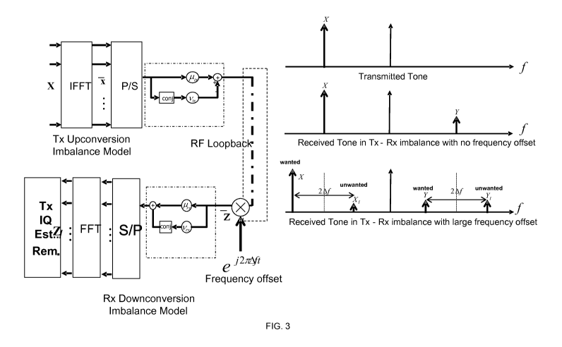
[0036] Figure 3 is a diagram illustrating an example of estimation of the
transmitter IQ imbalance in positive frequency offset. It will be understood
by those
of skill in the art that estimation of the transmitter IQ imbalance can also
be done
using negative frequency offset. Referring now to Figure 3, in one embodiment,
the
transmitter imbalance is estimated by sending an IQ probe that includes two
tones at
fixed locations. The large frequency offset allows for interference free
computation
of transmitter IQ imbalance parameters. For example, in one embodiment the
frequency offset is 1/10 the bandwidth. This is on the order of tens of bins
in some
systems.
[0037] In Figure 3 tones are illustrated as impulses. In actuality, each tone
and its images are sine functions. These sync functions have a main pulse
width of
2*bin-size. Additionally, the sine functions can interfere with each other if
they are
not separated in frequency. Accordingly, in one embodiment, the frequency
offset
can be selected to be large enough so that the image related to the receiver
IQ
imbalance is moved far away, in frequency, from the image of the transmitter
IQ
imbalance. By using an excess frequency offset the image ratio (YT/X) is a
close
approximation of the transmitter gain and total phase imbalance.
-- 10 --
CA 02724735 2010-11-17
WO 2010/002740 PCT/US2009/048923
[0038] As discussed above, because various embodiments of the systems and
methods described herein use a loopback any effects of the channel will be
negligible.
Accordingly, Ck = I. With Ck = 1 the signal 202 is X. =,Ll,Lle wt and the
signal
206 is Y. = ,u,xv e wt . Accordingly, the ratio of YT is:
XW
Y. _ ulve jOwt _ v
Ex JY x
'AX. ,urx,uewt flu
[0039] Figure 4 is a diagram illustrating estimation of the receiver IQ
imbalance. Referring now to Figure 4, by using the systems and methods
described
herein, the receiver imbalance can be computed independent of the transmitter
imbalance. This is done using an algorithm similar to the transmitter
imbalance
algorithm. By using an excess frequency offset the image ratio (YR/X*) is a
close
approximation of the transmitter gain and total phase imbalance. With Ck = 1
the
signal 208 is YR = v,p *e`cot and the signal 202 is X. = JlrxJtxe ret .
Accordingly
* -jAwt
YR _ J1txyrx _ V,
_ ~j
* jOwt * Erx I w
,urx
XW k PI
[0040] Figure 5 is a flowchart illustrating an example method in accordance
with various embodiments. Referring now to Figure 5, in a step 500, a device
is
configured to perform a self-characterization. In some embodiments, the self-
characterization can be performed over an RF loopback circuit. An example RF
loopback circuit is illustrated in Figures 3 and 4. As illustrated, a
transmitter in a
-- 11 --
CA 02724735 2010-11-17
WO 2010/002740 PCT/US2009/048923
communication device is connected to a receiver in the same device, allowing
the
device to characterize transmitter IQ imbalance, receiver IQ imbalance or
both.
[0041] In a step 502, a probe is transmitted over the RF loopback circuit. The
probe comprises a frequency offset such that an image related to one IQ
imbalance is
separated from an image related to another IQ imbalance. For example, in some
embodiments, a large frequency offset is used to limit the effect of transmit
imbalance
and receive imbalance. Accordingly, averaging is not needed to remove the
effects of
transmit or receive imbalance.
[0042] In a step 504, an imbalance estimate is calculated based on the probe
or
probes. For example, the imbalance estimate may include a gain imbalance, a
phase
imbalance, a delay imbalance or some combination of these. Additionally, in
one
embodiment, the imbalance estimate includes a transmitter IQ imbalance
estimate or a
receiver IQ imbalance estimate. The transmitter IQ imbalance and the receiver
IQ
imbalance can also be estimated simultaneously.
[0043] Various embodiments of the systems and methods described herein
may be used to estimate IQ imbalance, however, in some embodiments IQ
imbalance
can also be corrected. For example, IQ imbalance as seen at the receiving node
of an
OFDM communication link contains the combined effect of transmitter and
receiver
imbalances. It can be shown that every received tone paired with its image
(Z(k, l),
Z(-k, l), at subcarrier index k and symbol number l) at the receiver of an
OFDM
modem and after down conversion, is related to the pre-IQ distorted
transmitted tone
pair [X(k, l), X(-k, l), at subcarrier index k and symbol number 1] by:
-- 12 --
CA 02724735 2010-11-17
WO 2010/002740 PCT/US2009/048923
Z(k,1) K Y(k,1) -K CK X(k,1)
Z*(-k l) rx Y'(-k, l) rx tg X'(-k, I)
Y(k, l) X(k,l)
Y* (-k l) CK`,, X * (-k l) is the received signal before Rx IQ distortion and;
, ] ,
K,,, = 'u* vr* is the Rx IQ imbalance matrix and,
vrx /rx
Kt _ 'utx v, is the Tx IQ imbalance matrix,
Vtx P.
C C(k) C (-0 k) C(k) is the channel at tone index k and is assumed stationary.
0 ']
These parameters can be used to correct for various IQ imbalances in a
communication device.
[0044] Figure 6 is a diagram illustrating IQ imbalance correction at the
receiver. Referring now to Figure 6, a transmission block 600 includes a
transmitter
602 and a transmit IQ imbalance correction block 604. In various embodiments,
the
correction block 604 is used to remove the IQ imbalance caused by the
transmitter
602.
[0045] When signals * k, 1)) are input into transmitter 602 distorted
P(k, 1)
signals
P* (-k l) will be transmitted over the channel 612. Additionally, due to
I, ]
channel distortion, Y(k, 1)
Y (-k l) will be received at receive block 606. The receive
-- 13 --
CA 02724735 2010-11-17
WO 2010/002740 PCT/US2009/048923
block 606 includes a receive IQ imbalance correction block 608 and a receiver
610.
In various embodiments, the correction block 608 is used to correct for the IQ
imbalance that will be caused by the receiver 610. For example, the received
signals
can be transformed to Z(kZ (-, k l)l) in correction block 608.
L', ]
V
[0046] The transmit IQ distortion block 604 can be modeled as: u
vtx AX
V
and the receive IQ distortion block 608 can be modeled as: . Additionally,
vrx ,urx
the channel can be modeled as: C1 2 (k) 0
0 C12 (-k)
[0047] Accordingly, the received signals are:
Z(k,l) -K C K X(k,l)
Z*(-k 1) rx2 12 ~' [X* (-k, 1)
[0048] Due to the nature of this distortion which causes Inter-Carrier
Interference (ICI) in frequency domain, many algorithms jointly estimate and
remove
the effect of Tx-Rx IQ imbalance through performing some form of optimal, or
suboptimal, frequency domain equalization based on error minimization metrics
such
as least mean squared (LMS).
[0049] In some embodiments, correction is performed at the receive block 606
using equalization. One example error minimization metric is:
-- 14 --
CA 02724735 2010-11-17
WO 2010/002740 PCT/US2009/048923
KFn2 = (Krx2C12Ktx1) using this error minimization metric the effects of IQ
= KtX1C12'KrX2
imbalance can be removed: * (kk _ (Krx2C12Ktx1) 'Krx2C12Ktx1 X*(kk l)
( )
[0050] In some embodiments, the receive and transmit IQ imbalance can be
separated, estimated and compensated for separately. For example, in one
embodiment signals
X(k, 1) X'(-k l) are pre-compensated for using a pre-compensation
L, ]
matrix
(kk are transmitted using
I V, PI.x V . Accordingly the signals X"(-,l)]
,u transmit block 600. The signals 1,,* (kk l)] 1 are transmitted over the
channel 612.
V r
[0051] Compensation occurs at the receiver block 606 and the
Vr ,u
signal received at the receiver 610 R(k, 1) R*(-k l) is processed to determine
the correct
signal:
R(k,1) , , X(k,1) X(k,1)
= Krx2Krx2C~2K~x1Ktx1 = C12
L R(-k, l) Lx*_k,1] ) Lx*_k,1)
[0052] In some embodiments, delay imbalance and other frequency dependent
contributors, for example, e.g. in filters, can make IQ imbalance frequency
selective.
This results in different IQ distortion parameters on a per sub-carrier basis.
-- 15 --
CA 02724735 2010-11-17
WO 2010/002740 PCT/US2009/048923
[0053] As discussed above, some devices can simply estimate IQ imbalance
using the systems and methods described herein. Figure 7 is a diagram
illustrating an
example loopback in excessive frequency offset device 700. The device 700 of
Figure 7 does both IQ imbalance estimation and compensation in accordance with
one
embodiment. Referring now to Figure 7, the device 700 includes a block 702
which
represents a digital transmitter followed by the model of Tx IQ imbalance
distortion
704. The transmitter is used to transmit signals. These signals will have some
IQ
imbalance due to variations in frequency or amplitude between the I and Q
paths.
[0054] IQ imbalance for the signals can be corrected using correction block
708. The correction block performs the correction using information from an
estimation block 706. As illustrated in Figure 7, the cascade of transmitter
702 and
IQ impairment model 704 is coupled to the estimation block 706. This block
receives
the signals when the device 700 is operating in loopback mode. This allows the
device 700 to estimate IQ imbalance. Accordingly, it can provide correction
parameters to the correction block 708 so that corrections can be performed by
predistorting the transmitted signal.
[0055] Figure 8 is a diagram illustrating an example imbalance effect of a
single tone. Referring now to Figure 8, tone 800 is transmitted from the
transmitter as
an IQ probe. If there is no frequency offset between transmitter and receiver,
two
tones 802 and 804 will be received. It can be shown that the tone 802 will
have an
amplitude and phase scaled by (VrxC*kv: +,ufCk,uX) and the tone 804 has an
amplitude and phase scaled by (,urxC_kvx + vrxCk/J) .
-- 16 --
CA 02724735 2010-11-17
WO 2010/002740 PCT/US2009/048923
[0056] Due to frequency offset in the IQ transmit device, tone 800 will be
received as four tones 806, 808, 810 and 812 at the receive end. Tone 806 will
be
scaled by (v, c*kv ), tone 808 will be scaled by (,uCk,uX), tone 810 will by
scaled
by (v,Ck,utx) and tone 812 will be scaled by (,UYxC_kvj . Accordingly, it can
be
shown that YT ct - jox and YR EYx - j(OYx = Note that the above values are
XW XW
complex in general.
[0057] IQ imbalance can be classified into: amplitude imbalance and total
phase imbalance. In some embodiments, the total phase offset is made up of
frequency independent (constant) phase offset, sometimes simply referred to as
phase
offset and a frequency dependent (variable) phase offset, as a result of delay
imbalance.
[0058] Amplitude imbalance is calculated using a single probe. In some
embodiments, additional probes are used to update the amplitude imbalance
calculation or to average multiple amplitude imbalance calculations in order
to
average noise out. Amplitude imbalance is calculated as the real part of image-
to-
tone ratio. The image-to-tone ratio is the real part of the desired component
of the
received image divided by the desired component of the received tone.
Accordingly,
the amplitude imbalance on the transmit side is approximately: G = E Re Y
~ ~ ~X,
w
-- 17 --
CA 02724735 2010-11-17
WO 2010/002740 PCT/US2009/048923
Similarly, the amplitude imbalance on the receive side is approximately:
G,x = c, Re YR
XW
[0059] Figure 9 is a diagram illustrating computation of the IQ imbalance
parameters for phase and delay imbalance. It is assumed that two tones were
transmitted in bins Bx and Bxi and we have established the imaginary part of
image to
tone ratios as described above. This is done for each tone 900 and 906 and for
both
Tx as illustrated in the top diagram and Rx as illustrated in the bottom
diagram.
Referring now to Figure 9, the calculation of phase and delay imbalance is
discussed.
The total phase imbalance is illustrated as a line between two components 900
and
906. The total phase offset includes a portion that varies with frequency 902
and a
constant portion 904. Accordingly, the total phase offset, P, is equal to the
variable
phase offset, P, and the constant phase offset, P, or written as an equation:
PT = Py + P, The variable portion is a linear function of the frequency (Bin
number,
B) and the slope D, such that: Py = DB.
[0060] The total phase offset IQ imbalance on the transmit side is
approximately: PTtt -0 hn ~X~- This total phase offset IQ imbalance is made
W
up of a contribution from delay IQ imbalance (defined by slope D) and the
constant
phase offset. As illustrated in Figure 9, the IQ delay imbalance is the slope
of line
902 and the constant phase offset is defined by the line 954. The delay IQ
imbalance
on the transmit side is equal to the slope, which is:
-- 18 --
CA 02724735 2010-11-17
WO 2010/002740 PCT/US2009/048923
Im Y1T - lm YT
X1W XW
Slope = D, = The constant phase offset, referred to as the
BX1 - BX
phase offset is: Pc, = PT tt - BXD,
[0061] For the receive IQ imbalance, probe ratios 950 and 956 can be used to
calculate IQ imbalance, including the total phase offset 952 and the constant
phase
offset 954. Similarly to the transmit imbalance equations:
~j YR
P7x -Y'rx Im
XW
Im Y1R* -Im YR*
Slope = D, = X1W XW
BXi - Bx
PC, =PT -BXD,x
[0062] Figure 10 is a flowchart illustrating a method in accordance with the
systems and methods described herein. Referring now to Figure 10, IQ imbalance
is
computed by first transmit a probe in a step 1000. The probe may include M
symbols,
for example, M may be 4-8 symbols. In some embodiments, each symbol comprises
a single tone per symbol at bin number Bx. The bin number in some embodiments
may be approximately -140. By transmitting a series of probes ratios and
average
over M for YR / (Xw)* and YT / Xw can be determine.
-- 19 --
CA 02724735 2010-11-17
WO 2010/002740 PCT/US2009/048923
[0063] A second probe is then transmitted in a step 1002. The probe includes
N symbols. N is generally smaller than M when the frequency offset is
negative, for
example, N - M-4. Conversely, N is generally larger than M when the frequency
offset is positive, for example, N - M+4 symbols. In some embodiments, each
symbol constitutes a single tone per symbol. The bin number in some
embodiments is
approximately 140 (or -Bx). By transmitting a series of probes ratios and
average
over N, YR / (Xw)* and YT / Xw can be determined.
[0064] In a step 1004, gain, phase and delay imbalances are computed (G, Pc,
D or I, Q and D respectively) for both Tx and Rx. In various embodiments,
gain,
phase and delay imbalances are computed as described with respect to Figure 9.
Additionally, in some embodiments where the loopback channel cannot be
approximated as constant, the systems and methods described herein can switch
between positive and negative spectrum when transmit probes.
[0065] The systems and methods described herein can be used to compute IQ
imbalance in a communication system. For example, these systems and methods
may
be applied to an OFDM communication system. In various embodiments, IQ
imbalances can be corrected. For example, some embodiments use pre-distortion
to
correct for transmit IQ imbalance. Additionally, some embodiments use post
distortion to correct for receive IQ imbalance. Other embodiments use both pre-
distortion and post distortion so that transmit and receive IQ imbalance is
corrected.
[0066] Pre-distortion can be modeled as:
c, (k) = d, (k) - v )d,* (-k)
flu
-- 20 --
CA 02724735 2010-11-17
WO 2010/002740 PCT/US2009/048923
YA v E - J~0
X B /tx x
where N is the FFT size. Figure 11 is a diagram illustrating correction
hardware that
can be used for frequency domain transmit pre-distortion in an OFDM system. As
illustrated in Figure 11, the correction hardware pre-distorts the on input I
an Q values
according to the estimated Gain, (G), Phase (Pc) and Delay (D) values. This
predistortion is effectively equivalent to multiplication of the inverse of
transmit IQ
imblalance by the data.
[0067] An example of post distortion can be modeled by the following
transform operating on the distorted data b'(t):
c(t) = b'(t) - v b" (t)
j'rx
Y Vrx 1(t~
X* Erx / Y'rx
Px
[0068] Figure 12 is a diagram illustrating correction hardware that can be
used
for receive post distortion. As illustrated in Figure 12, the correction
hardware
corrects the effect of receiver delay imbalance by effectively applying the
inverse of
receiver imbalance matrix to the down converted Data. Assuming no frequency
dependent imbalance component, this example performs correction in time domain
and prior to the FFT at the receiver. If the imbalance is frequency dependent
the
-- 21 --
CA 02724735 2010-11-17
WO 2010/002740 PCT/US2009/048923
correction can be performed in frequency domain after the FFT. Pre-distortion
and
post distortion are generally understood by those of skill in the art and, for
brevity,
will not be discussed further here.
[0069] Figure 13 is a diagram illustrating a loopback system. The diagram is
used to discuss an example algorithm for channel dependent loopback for
receive IQ
imbalance computations. Figure 13 is similar to Figure 3; however, in this
example
the equations further illustrate the effects of a channel. Referring now to
Figure 13,
the wanted signal is modeled as X, = ,u,xCk,utXe' wt where Ck models the
channel,
which in this example is not assumed to be 1. The unwanted signal is modeled
as
Xj = v,xC*kvt e+' wt where C*k models the channel. Similarly, YR = v,xCk,u e'
wt,
again, the channel, Ck , in this example is not assumed to be 1. The unwanted
signal
is modeled as Y. = ,uSkve ' wt where C k models the channel. Accordingly,
jAwt
YR _ xCky x _ Ck Vr = v E - jcp, As will be clear to those of skill in
X, [ Ckptx jOwt 1 * Ck*JI Prx
the art, the receive IQ imbalance is generally channel independent. In other
words,
YR
does not depend on the channel. In general, Ck can be complex (having real
XW
and imaginary components.)
[0070] Figure 14 is a diagram illustrating a loopback system. The diagram is
used to discuss an example algorithm in which two symbols are transmitted in
order
to perform a transmit IQ imbalance computation when the loopback channel is
not
constant (Ck :~1). In order to eliminate the effect of the channel the ratio
of the image
-- 22 --
CA 02724735 2010-11-17
WO 2010/002740 PCT/US2009/048923
of a first symbol to the tone of a second symbol is calculated. For example,
in some
embodiments, symbol type "A" represents a transmit at a negative tone and
symbol
type "B" represents a transmit at a positive tone. As illustrated in Figure
14, the ratio
of symbol A to tone B is calculated. In various other embodiments the ratio of
symbol B to tone A is calculated.
[0071] The wanted portions of symbol A are modeled as X' _ ,u~Ck ,utxe ' ,'t
and YT = ,uCkvtxe ' o t . The unwanted portions of symbol A are modeled as
X 'A = v,xC'kv e+1 0t and RA = vrxC;A u:e' w" . From these signals it can be
shown that
A ;owt B B
YT _ /J C kytxe _ Ck yx = Gk yx A B
B B jOwt B B- J(ptx since C -k Ck
XW pr Ck ptxe Ck ptx Ck ptx
[0072] While various embodiments of the disclosed method and apparatus
have been described above, it should be understood that they have been
presented by
way of example only, and not of limitation. Likewise, the various diagrams may
depict an example architectural or other configuration for the disclosed
method and
apparatus, which is done to aid in understanding the features and
functionality that
can be included in the disclosed method and apparatus. The disclosed method
and
apparatus is not restricted to the illustrated example architectures or
configurations,
but the desired features can be implemented using a variety of alternative
architectures and configurations. Indeed, it will be apparent to one of skill
in the art
how alternative functional, logical or physical partitioning and
configurations can be
implemented to implement the desired features of the disclosed method and
apparatus.
Also, a multitude of different constituent module names other than those
depicted
-- 23 --
CA 02724735 2010-11-17
WO 2010/002740 PCT/US2009/048923
herein can be applied to the various partitions. Additionally, with regard to
flow
diagrams, operational descriptions and method claims, the order in which the
steps are
presented herein shall not mandate that various embodiments be implemented to
perform the recited functionality in the same order unless the context
dictates
otherwise.
[0073] Although the disclosed method and apparatus is described above in
terms of various exemplary embodiments and implementations, it should be
understood that the various features, aspects and functionality described in
one or
more of the individual embodiments are not limited in their applicability to
the
particular embodiment with which they are described, but instead can be
applied,
alone or in various combinations, to one or more of the other embodiments of
the
disclosed method and apparatus, whether or not such embodiments are described
and
whether or not such features are presented as being a part of a described
embodiment.
Thus, the breadth and scope of the claimed invention should not be limited by
any of
the above-described exemplary embodiments.
[0074] Terms and phrases used in this document, and variations thereof,
unless otherwise expressly stated, should be construed as open ended as
opposed to
limiting. As examples of the foregoing: the term "including" should be read as
meaning "including, without limitation" or the like; the term "example" is
used to
provide exemplary instances of the item in discussion, not an exhaustive or
limiting
list thereof; the terms "a" or "an" should be read as meaning "at least one,"
"one or
more" or the like; and adjectives such as "conventional," "traditional,"
"normal,"
"standard," "known" and terms of similar meaning should not be construed as
-- 24 --
CA 02724735 2010-11-17
WO 2010/002740 PCT/US2009/048923
limiting the item described to a given time period or to an item available as
of a given
time, but instead should be read to encompass conventional, traditional,
normal, or
standard technologies that may be available or known now or at any time in the
future. Likewise, where this document refers to technologies that would be
apparent
or known to one of ordinary skill in the art, such technologies encompass
those
apparent or known to the skilled artisan now or at any time in the future.
[0075] A group of items linked with the conjunction "and" should not be read
as requiring that each and every one of those items be present in the
grouping, but
rather should be read as "and/or" unless expressly stated otherwise.
Similarly, a
group of items linked with the conjunction "or" should not be read as
requiring
mutual exclusivity among that group, but rather should also be read as
"and/or" unless
expressly stated otherwise. Furthermore, although items, elements or
components of
the disclosed method and apparatus may be described or claimed in the
singular, the
plural is contemplated to be within the scope thereof unless limitation to the
singular
is explicitly stated.
[0076] The presence of broadening words and phrases such as "one or more,"
"at least," "but not limited to" or other like phrases in some instances shall
not be read
to mean that the narrower case is intended or required in instances where such
broadening phrases may be absent. The use of the term "module" does not imply
that
the components or functionality described or claimed as part of the module are
all
configured in a common package. Indeed, any or all of the various components
of a
module, whether control logic or other components, can be combined in a single
-- 25 --
CA 02724735 2010-11-17
WO 2010/002740 PCT/US2009/048923
package or separately maintained and can further be distributed in multiple
groupings
or packages or across multiple locations.
[0077] Additionally, the various embodiments set forth herein are described in
terms of exemplary block diagrams, flow charts and other illustrations. As
will
become apparent to one of ordinary skill in the art after reading this
document, the
illustrated embodiments and their various alternatives can be implemented
without
confinement to the illustrated examples. For example, block diagrams and their
accompanying description should not be construed as mandating a particular
architecture or configuration.
-- 26 --