Note: Descriptions are shown in the official language in which they were submitted.
CA 02724875 2010-11-18
WO 2009/143284 PCT/US2009/044726
OPTO-ISOLATOR MULTI-VOLTAGE DETECTION CIRCUIT
FIELD OF THE INVENTION
[0001] The present invention relates to voltage detection devices and, more
particularly, to
an opto-isolator multi-voltage detection circuit that provides voltage
detection.
BACKGROUND
[0002] There exists a wide variety of power sources for powering electronic
devices. For
example, in the United States and Japan the standard AC voltage is 110V, while
the AC
standard voltage in Europe, Australia and other countries is 240V. When
connecting an
electronic device to a power source or any electric circuit, it may be
beneficial to confirm the
presence of the required voltage to the electronic device.
[0003] Presently, available low voltage detector circuits are used to detect
the presence of a
voltage from a power source. An opto-isolator is an electrical component
typically used in a
low voltage detector circuit to optically transfer a signal between an input
and an output
circuit, such as between a low voltage and a high voltage circuit. The opto-
isolator helps to
electromagnetically isolate the circuits from one another and from potentially
destructive
voltage spikes. Unlike a voltage transformer, an opto-isolator removes ground
loops and
excess noise or electromagnetic interference (EMI), and provides protection
from serious
over voltage conditions. Generally, a voltage detector circuit includes an
opto-isolator to
detect the presence of a voltage, and also includes a sensing resistor in
series with the opto-
isolator. The use of the sensing resistor may be undesirable in some
applications because the
resistor must handle an excessive power dissipation which leads to high
impedance noise
pulses. Unfortunately, a sensing resistor is expensive, and typically
dissipates a substantial
amount of heat.
SUMMARY OF THE INVENTION
[0004] According to one aspect of the invention, an opto-isolator multi-
voltage detection
circuit for use with 9 volt DC through 240 volt AC input voltages from a
voltage source
1
CA 02724875 2010-11-18
WO 2009/143284 PCT/US2009/044726
includes an opto-isolator, a diode connected to the voltage source, and a
first transistor. The
opto-isolator is configured to detect the presence of the voltage source and
current flowing
forward from the diode biases a light-emitting diode (LED) of the opto-
isolator, and
consequently any power dissipated through the first transistor in response to
the input voltage
is maintained at or below an acceptable level.
[0005] The opto-isolator multi-voltage detection circuit may further
incorporate a
converter such as a DC to DC converter. The DC to DC converter may provide the
further
benefit of reducing system crosstalk and power dissipation.
[0006] The opto-isolator multi-voltage detection circuit may further
incorporate a second
transistor and a voltage divider. The voltage divider may be operatively
coupled to the first
and second transistors and is configured to divide the input voltage across
the first and second
transistors. The voltage divider may provide the further benefit of reducing
the power
dissipated through the first and second transistors.
[0007] According to another aspect of the invention, an opto-isolator multi-
voltage
detection circuit for use with 9 volt DC through 240 volt AC input voltages
from a voltage
source includes a diode, first and second transistors, two zener diodes, and
an opto-isolator
coupled to the first and second transistors. The zener diodes may limit the
input voltage to
the first and second transistors providing an overall reduction in power
dissipation and
system crosstalk.
[0008] According to another aspect of the invention, an opto-isolator multi-
voltage
detection circuit for use with 9 volt DC through 240volt AC input voltages
from a voltage
source includes a rectifier connected to the voltage source, an opto-isolator,
first and second
transistors, a voltage divider coupled to the first and second transistors,
and a converter
connected to the second transistor and the opto-isolator. The voltage divider
is configured to
divide the input voltage across the first and second transistors. The
converter, such as a DC
2
CA 02724875 2010-11-18
WO 2009/143284 PCT/US2009/044726
to DC converter, is configured to maintain an output current from the
rectifier. When the
output current from the rectifier forward biases a light-emitting diode (LED)
of the opto-
isolator, the first and second transistors are configured to reduce a power
dissipated through
the circuit such that a power dissipation of the first and second transistors
is different from
the power dissipated through the circuit.
BRIEF DESCRIPTION OF THE DRAWINGS
[0009] For a more complete understanding of the disclosure, reference should
be made to
the following detailed description and accompanying drawings wherein:
[0010] FIG. I is a perspective view of an opto-isolator multi-voltage
detection device that
may be used to connect any one of a variety of electronic devices to a voltage
source;
[0011] FIG. 2 is a schematic illustration of an opto-isolator multi-voltage
detection device
assembled in accordance with the teachings of the invention;
[0012] FIG. 3 is a schematic illustration of another embodiment of an opto-
isolator multi-
voltage detection device assembled in accordance with the teachings of the
invention;
[0013] FIG. 4 is a schematic illustration of another embodiment of an opto-
isolator multi-
voltage detection device assembled in accordance with the teachings of the
invention;
[0014] FIG. 5 is a schematic illustration of another embodiment of an opto-
isolator multi-
voltage detection device assembled in accordance with the teachings of the
invention; and
[0015] FIG. 6 is a schematic illustration of another embodiment of an opto-
isolator multi-
voltage detection device assembled in accordance with the teachings of the
invention.
3
CA 02724875 2010-11-18
WO 2009/143284 PCT/US2009/044726
DETAILED DESCRIPTION
[0016] FIG. 1 schematically depicts an exemplary opto-isolator multi-voltage
detection
circuit 10 assembled in accordance with the teachings of the invention. The
circuit 10 may
be used to connect any one of a variety of electronic devices to a voltage
source 12. The
circuit 10 may be a stand-alone circuit that connects virtually any type of
electronic device to
a socket 12a of the voltage source 12. Alternatively, the circuit 10 may be a
built-in circuit
disposed inside the electronic device, with the electronic device directly
connectable to the
socket 12a. Exemplary electronic devices include a hair dryer 14, a shaver 16,
a vacuum
cleaner 18 or other consumer electronic devices.
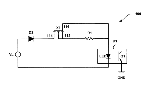
[0017] FIG. 2 depicts an exemplary opto-isolator multi-voltage detection
circuit 100
assembled in accordance with the teachings of the invention. The circuit 100
includes an
opto-isolator D1, which is preferably part number HCPL-2360, as sold by Avago
Technologies Limited. Typically, the opto-isolator D1 includes a light
emitting diode LED
and a phototransistor Q1. When using the preferred opto-isolator, the opto-
isolator can detect
current ranging from about 1.2mA to about 50mA. Other sizes may be chosen in
order to
detect current across a different range. In turn, the current drives the LED
to light. The
circuit 100 further includes a diode D2, a resistor R1, and a transistor X1.
The transistor X1
may be an N-channel depletion field-effect transistor (FET), which is
preferably part number
BSS 139, as sold by Infineon Technologies AG. The transistor Xl has a source
terminal 112,
a drain terminal 114, and a gate terminal 116. The diode D2, which may be a
surface mount
standard recovery power rectifier diode, is connected to the drain terminal
114 of the
transistor X1. The diode D2 is preferably part number MRA4007T3, as sold by
Semiconductor Components Industries, LLC. The gate terminal 116 of the
transistor XI and
one end of the resistor RI are connected to one end of the opto-isolator Dl.
The other end of
the opto-isolator D1 is connected to a ground GND. The source terminal 112 of
the transistor
4
CA 02724875 2010-11-18
WO 2009/143284 PCT/US2009/044726
Xl is connected to the other end of the resistor R1. The resistor RI is
preferably 768ohm,
although other resistance values are contemplated. An input V,,, is connected
to the diode D2.
[0018] Operation of the circuit 100 is now described. The circuit 100 is used
to handle a
wide range of input voltages ranging from about 9 volt DC through 240 volt AC
in
accordance with the teachings of the invention. For example, when an input of
approximately 250 Vac rms (approximately 350 Vac peak) is applied to the
circuit 100, a
current starts to flow through the diode D2, the transistor X 1, the resistor
R 1, and the opto-
isolator D1. As a result, the current that flows through the opto-isolator D 1
ranges from
about 1.3mA to about 2.7mA, thereby causing the LED of the opto-isolator Dl to
light. A
voltage Vgs across the transistor X1 ranges from about -lvolt to about -
2.1volts.
Consequently, a power dissipated through the transistor X1 is approximately
338mW, which
is marginally close to the power rating (360mW) of the transistor X1.
[0019] To further reduce the power dissipation, the transistor X1 may be
larger than the
exemplary BSS 139 transistor discussed above. For example, the transistor X1
may be part
number BSS 126, as sold by Infineon Technologies AG, which has a higher power
of about
500mW and a higher voltage Vds of about 600volts. A larger resistor also may
be used. One
exemplary larger resistor may have a resistance of about 1.23kohms. When the
larger
transistor and resistor are used and an input of approximately 250 Vac rms
(approximately
350 Vac peak) is applied to the circuit 100, a current starts to flow through
the diode D2, the
transistor, the resistor, and the opto-isolator D1. As a result, the current
that flows through
the opto-isolator D1 ranges from about 1.3mA to about 2.2mA and a voltage Vgs
across the
transistor ranges from about -1.6volts to about -2.7volts. Consequently, the
power dissipated
through the transistor is approximately 275mW, which is half of the power
rating (500mW)
of the transistor. Again, the use of the high power and high voltage
transistor may provide
the further benefit of reducing a power dissipated through the transistor Xl.
CA 02724875 2010-11-18
WO 2009/143284 PCT/US2009/044726
[0020] FIG. 3 depicts an opto-isolator multi-voltage detection circuit 200
assembled in
accordance with the teachings of another exemplary embodiment of the
invention. The
circuit 200 includes an opto-isolator D1, which is preferably part number HCPL-
2360, as
sold by Avago Technologies Limited. Typically, the opto-isolator DI includes a
light
emitting diode LED and a phototransistor Q1. When using the preferred opto-
isolator, the
opto-isolator again can detect the current ranging from about 1.2mA to about
50mA, and the
current again drives the LED to light. The circuit 200 further includes a
diode D2, a resistor
R1, a transistor Xl, and a DC to DC converter 218. The transistor X1 may be
the N-channel
depletion field-effect transistor (FET), which is the BSS 139 transistor sold
by Infineon
Technologies AG discussed above. The transistor X1 has a source terminal 212,
a drain
terminal 214, and a gate terminal 216. The diode D2, such as a surface mount
standard
recovery power rectifier diode, is connected to the drain terminal 214 of the
transistor Xl.
The diode D2 is preferably part number MRA4007T3, as sold by Semiconductor
Components Industries, LLC. The gate terminal 216 of the transistor Xl is
connected to one
end of the resistor R1 and to a first end 218a of the DC to DC converter 218.
A second end
218b of the DC to DC converter 218 is connected to the source terminal 212 of
the transistor
X I. A third end 218c of the DC to DC converter 218 is connected to the other
end of the
resistor R1 and to one end of the opto-isolator D1. The other end of the opto-
isolator D1 is
connected to a ground GND. The resistor RI in this case is preferably much
larger with
respect to the resistor in FIG. 1. The resistor R1 is preferably 3.8kohm,
although other
resistance values are contemplated. The DC to DC converter 218 is preferably
rated at
5volts, although other voltage values are contemplated. An input Vin is
connected to the
other end of the diode D2.
[0021] Operation of the circuit 200 is now described. The circuit 200 is used
to handle a
wide range of input voltages ranging from about 9 volt DC through 240 volt AC
in
accordance with the teachings of the invention. For example, when an input of
6
CA 02724875 2010-11-18
WO 2009/143284 PCT/US2009/044726
approximately 250 Vac rms (approximately 350 Vac peak) is applied to the
circuit 200, a
current starts to flow through the diode D2, the transistor Xl, the resistor
RI, the DC to DC
converter 218, and the opto-isolator D1. As a result, the DC to DC converter
keeps the
current that flows through the opto-isolator Dl at approximately 1.3mA. The DC
to DC
converter also keeps the power dissipation at the transistor XI at
approximately 163mW
which is below the power rating (360mW) of the transistor. The use of the DC
to DC
converter 218 may provide the benefit of maintaining the current flow through
the circuit 100
thus providing an overall reduction in system crosstalk and power dissipation.
[0022] FIG. 4 depicts an opto-isolator multi-voltage detection circuit 300
assembled
according to the teachings of yet another exemplary form of the invention. The
circuit 300
includes an opto-isolator D1, which is preferably the Avago Technologies
Limited part
number HCPL-2360 discussed above. The opto-isolator Dl includes a light
emitting diode
LED and a phototransistor Q1. Once again, when using the preferred opto-
isolator, the opto-
isolator can detect the current ranging from about 1.2mA to about 50mA. The
circuit 300
further includes a diode D2, a first zener diode Z1, a second zener diode Z2,
a first resistor
R1, a second resistor R2, a first transistor XI, and a second transistor X2.
The first and
second transistors Xl, X2 connected in series preferably are N-channel
depletion field-effect
transistors (FETs) which again may be part number BSS139, as sold by Infineon
Technologies AG. The first transistor X1 has a source terminal 312, a drain
terminal 314,
and a gate terminal 316. The second transistor X2 also has a source terminal
320, a drain
terminal 322, and a gate terminal 324. The diode D2, such as a surface mount
standard
recovery power rectifier diode, is connected to the drain terminal 322 of the
transistor X2 and
to one end of the zener Z1. The other end of the zener Z1 is connected to the
source terminal
320 of the transistor X2 and to one end of the resistor R2. The other end of
the resistor R2 is
connected to the gate terminal 324 of the transistor X2. The diode D2 is
preferably the part
7
CA 02724875 2010-11-18
WO 2009/143284 PCT/US2009/044726
number MRA4007T3 discussed above and made by Semiconductor Components
Industries,
LLC. An input Vin is connected to the other end of the diode D2.
[0023] One end of the zener diode ZI is connected to the drain terminal 314 of
the
transistor X1. The other end of the zener diode Zl is connected to the source
terminal 312 of
the transistor X 1 and to one end of the resistor R 1. The other end of the
resistor R 1 is
connected to the gate terminal 316 of the transistor X1 and to one end of the
opto-isolator D1.
The other end of the opto-isolator D1 is connected to a ground GND. The
resistor R1 in this
case is preferably 768ohm, while the resistor R2 is preferably 750ohm,
although other
resistance values are contemplated. The zener diodes Z1, Z2 are preferably
part number
1SMB5952BT3, as sold by Semiconductor Components Industries LLC, and have
voltage
and power ratings of 130volts and 3watts. Other voltage and power ratings are
contemplated.
[0024] Operation of the circuit 300 is now described. With the addition of the
second
transistor X2 and the zener diodes Z1, Z2, when an input of approximately 250
Vac rms
(approximately 350 Vac peak) is applied to the circuit 300, a current starts
to flow through the
diode D2, the transistors Xl, X2, the zener diodes Z1, Z2, the resistors R1,
R2, and the opto-
isolator Dl. As a result, the voltage measured across the transistors X1, X2
is below peak
voltage (approximately 180volts), while the current that flows through the
opto-isolator Dl
varies from about 1.3mA to about 2.7mA. This yields a power dissipation of
173mW for the
transistors X1, X2. The use of the zener diodes Zl, Z2 may provide the benefit
of limiting
the input voltage to the first and second transistors X1, X2. The use of the
transistors X1, X2
may provide the benefit an overall reduction in system crosstalk and power
dissipation.
[0025] FIG. 5 depicts an opto-isolator multi-voltage detection circuit 400
assembled in
accordance with the teachings of yet another example of the invention. The
circuit 400
includes an opto-isolator D 1, which again is preferably part number HCPL-
2360, as sold by
Avago Technologies Limited. Typically, the opto-isolator D1 includes a light
emitting diode
8
CA 02724875 2010-11-18
WO 2009/143284 PCT/US2009/044726
LED and a phototransistor Q1. The preferred opto-isolator can detect the
current ranging
from about 1.2mA to about 50mA, and in turn the current drives the LED to
light. The
circuit 400 further includes a diode D2, a capacitor Cl, a first resistor R 1,
a second resistor
R2, a third resistor R3, a fourth resistor R4, a first transistor X1, and a
second transistor X2.
The diode D2, resistor R2, and capacitor Cl constitute a rectifier 438 while
resistors R3 and
R4 constitute a voltage divider 440. The first and second transistors Xl, X2
connected in
series again may be the foregoing N-channel depletion field-effect transistors
(FETs). The
first transistor X1 has a source terminal 412, a drain terminal 414, and a
gate terminal 416.
The second transistor X2 also has a source terminal 420, a drain terminal 422,
and a gate
terminal 424. The diode D2, such as a surface mount standard recovery power
rectifier
diode, is connected to one end of the resistor R2. An input Vin is connected
to the other end
of the diode D2. The other end of the resistor R2 is connected to one end of
the capacitor C 1
and to the drain terminal 422 of the transistor X2. The other end of the
capacitor C I is
connected to a ground GND. The capacitor Cl preferably has a capacitance of
0.01
although different values are contemplated.
[0026] The source terminal 420 of the transistor X2 is connected to the drain
terminal 414
of the transistor X1. The gate terminal 424 of the transistor X2 connects the
resistor R3 to
the resistor R4. The other end of the resistor R3 is connected to the drain
terminal 422 of the
transistor X2. The source terminal 412 of the transistor Xl is connected to
one end of the
resistor R1. The other end of the resistor RI is connected to the gate
terminal 416 of the
transistor Xl and to one end of the opto-isolator Dl. The other end of the
opto-isolator D1 is
connected to a ground GND. The resistor RI again preferably has a resistance
of 768ohms,
while the resistance of the rest of the resistors R2, R3, R4 may be, for
example, 1Mohm,
respectively, although other resistance values are contemplated.
[0027] Operation of the circuit 400 is now described. When an input of
approximately 250
Vac rms (approximately 350 Vac peak) is applied to the circuit 400, a current
starts to flow
9
CA 02724875 2010-11-18
WO 2009/143284 PCT/US2009/044726
through the diode D2, the transistors Xl, X2, the resistors R1, R2, R3, R4,
and the opto-
isolator D1. In this configuration, the current that flows through the opto-
isolator DI varies
from approximately 1.3mA to approximately 2.7mA. Advantageously, the use of
the voltage
divider 440 to the transistors XI, X2 provides the benefit of evenly dividing
the input voltage
across the transistors X1, X2 at approximately half of the peak voltage
(approximately
125volts). This yields a power dissipation of approximately 169mW for the
transistors X1,
X2. Thus, zener diodes are no longer required.
[0028] FIG. 6 depicts an opto-isolator multi-voltage detection circuit 500
assembled in
accordance with the teachings of a still further example of the invention. The
circuit 500
includes an opto-isolator D1, which is preferably the HCPL-2360 opto-isolator
discussed
above by Avago Technologies Limited which is capable of detecting a current
ranging from
about 1.2mA to about 50mA. Typically, the opto-isolator D1 includes a light
emitting diode
LED and a phototransistor Q1. The LED lights when the current ranging from
about 1.2mA
to about 50mA flows through the opto-isolator D1. The circuit 500 further
includes a diode
D2, a capacitor Cl, a first resistor R1, a second resistor R2, a third
resistor R3, a fourth
resistor R4, a first transistor XI, a second transistor X2, and a DC to DC
converter 518. The
diode D2, the resistor R2, and the capacitor Cl constitute a rectifier 538
while the resistors
R3, R4 constitute a voltage divider 540. The first and second transistors X1,
X2, connected
in series, again may be the N-channel depletion field-effect transistors
(FETs) discussed
above and sold by Infineon Technologies AG. The first transistor Xl has a
source terminal
512, a drain terminal 514, and a gate terminal 516. The second transistor X2
also has a
source terminal 520, a drain terminal 522, and a gate terminal 524. The diode
D2, which may
be a surface mount standard recovery power rectifier diode, is connected to
one end of the
resistor R2. An input V,,, is connected to the other end of the diode D2. The
other end of the
resistor R2 is connected to one end of the capacitor Cl and to the drain
terminal 522 of the
transistor X2. The other end of the capacitor C l is connected to a ground
GND. The
CA 02724875 2010-11-18
WO 2009/143284 PCT/US2009/044726
capacitor Cl has a capacitance of preferably 0.01 , although different values
are
contemplated.
[0029] The source terminal 520 of the transistor X2 is connected to the drain
terminal 514
of the transistor X1. The gate terminal 524 of the transistor X2 connects the
resistor R3 to
the resistor R4. The other end of the resistor R3 is connected to the drain
terminal 522 of the
transistor X2. The source terminal 512 of the transistor Xl is connected to a
second end 518b
of the DC to DC converter 518. The gate terminal 516 of the transistor X1 is
connected to a
first end 518a of the DC to DC converter 518 and to one end of the resistor R
I. The third end
518c of the DC to DC converter 518 is connected to the other end of the
resistor R1 and to
one end of the opto-isolator D1. The other end of the opto-isolator Dl is
connected to a
ground GND. The resistor RI in this case preferably has a resistance of about
3.8kohm,
while the rest of the resistors R2, R3, R4 preferably have a resistance of
about 1Mohm. The
DC to DC converter 518 is preferably rated at 5volts, although other voltage
values are
contemplated.
[0030] Operation of the circuit 500 is now described. When an input of
approximately
250 Vac rms (approximately 350 Vac peak) is applied to the circuit 500, a
current starts to flow
through the diode D2, the transistors X1, X2, the resistors R1, R2, R3, R4,
the DC to DC
converter 518, and the opto-isolator DI. In this configuration, the voltage
divider 540 evenly
divides the input voltage across the transistors Xl, X2, while the DC to DC
converter 518
maintains the current that flows through the opto-isolator D1 at approximately
1.3mA.
Advantageously, the use of the transistors X1, X2 and the DC to DC converter
518 provide
the benefit of yielding the power dissipation at approximately 82mW. The use
of the DC to
DC converter 518 and the voltage divider 540 may provide benefit of
maintaining the current
flow through the circuit providing an overall reduction in system crosstalk
and power
dissipation.
11
CA 02724875 2010-11-18
WO 2009/143284 PCT/US2009/044726
[0031] When assembled in accordance with one or more of the example described
herein,
the opto-isolator multi-voltage detection circuit may provide the benefit of
maintaining a
current providing an overall reduction in power dissipation and system
crosstalk. The circuit
also may provide further benefit of evenly dividing an input voltage providing
a further
reduction in power dissipation and system crosstalk.
[0032] The preceding text sets forth a detailed description of numerous
different
embodiments of the invention, it should be understood that the legal scope of
the invention is
defined by the words of the claims set forth at the end of this patent. The
detailed description
is to be construed as exemplary only and does not describe every possible
embodiment of the
invention since describing every possible embodiment would be impractical, if
not
impossible. For example, it should be appreciated that the embodiments
disclosed in FIG. 2
through FIG. 4 with provide constant excitation of the opto-isolator when the
presence of a
DC voltage is detected. However, the cyclic nature of an AC voltage will
intermittently
switch the opto-isolator (i.e. periodically excite the opto-isolator) in
accordance with the
periodicity of the signal. In the alternative, the embodiments of FIG. 5 and
FIG. 6 will
provide constant excitation; even in the presence of an AC signal due to the
rectifying nature
of capacitor Cl. Numerous alternative embodiments could be implemented, using
either
current technology or technology developed after the filing date of this
patent, which would
still fall within the scope of the claims defining the invention.
12