Note: Descriptions are shown in the official language in which they were submitted.
CA 02724951 2015-07-17
METHOD OF FORMING STABLE FUNCTIONALIZED NANOPARTICLES
BACKGROUND OF THE INVENTION
1. Field of the Invention
The present invention relates to methods for the mechanochemical preparation
of
stable passivated nanoparticles, made of e.g. silicon or germanium.
2. General Background of the Invention
A nanoparticle (or nanopowder) is a microscopic particle with at least one
dimension less than 100 nanometer (nm). Nanoparticles have recently been at
the
forefront of biomedical, optical, and electronics research because they can
exhibit
fundamentally new behavior when their sizes fall below the critical length
scale
associated with any given property. A bulk material is generally considered to
have
- 1 -
CA 02724951 2010-11-19
WO 2009/011981 PCT/US2008/065534
uniform physical properties throughout regardless of its size, but at the nano-
scale the
properties of materials change as the percentage of atoms at the surface of
the material
becomes significant. Below the micrometer scale, size-dependent properties are
observed
such as quantum confinement in semiconductor particles, surface plasmon
resonance in
some metal particles, and supermagnetism in magnetic materials.
Quantum confinement occurs when electrons and holes in a semiconductor are
restricted in one or more dimensions. A quantum dot is confined in all three
dimensions, a
quantum wire is confined in two dimensions, and a quantum well is confined in
one
dimension. That is, quantum confinement occurs when one or more of the
dimensions of
1 0 a nanocrystal is made very small so that it approaches the size of an
exciton in bulk
crystal, called the Bohr exciton radius. An exciton is a bound state of an
electron and an
imaginary particle called an electron hole in an insulator or semiconductor.
An exciton is
an elementary excitation, or a quasiparticle of a solid. A quantum dot is a
structure where
all dimensions are near the Bohr exciton radius, typically a small sphere. A
quantum wire
is a structure where the height and breadth is made small while the length can
be long. A
quantum well is a structure where the height is approximately the Bohr exciton
radius
while the length and breadth can be large. Quantum confinement effects at very
small
crystalline sizes can cause silicon and germanium nanoparticles to fluoresce,
and such
fluorescent silicon and germanium nanoparticles have great potential for use
in optical
2 0 and electronic systems as well as biological applications.
Silicon and germanium nanoparticles may be used, e.g., in optical switching
devices, photovoltaic cells, light emitting diodes, lasers, and optical
frequency doublers,
and as biological markers.
The photoluminescence (PL) mechanism in silicon and germanium nanoparticles
is also influenced by the nature and bonding state of the particle surface.
Photoluminescence is a process in which a chemical compound absorbs photons
(electromagnetic radiation), thus transitioning to a higher electronic energy
state, and then
radiates photons back out, returning to a lower energy state. The period
between
absorption and emission is typically extremely short, on the order of 10
nanoseconds.
Under special circumstances, however, this period can be extended into minutes
or hours.
Ultimately, available chemical energy states and allowed transitions between
states (and
-2-
CA 02724951 2010-11-19
WO 2009/011981 PCT/US2008/065534
therefore wavelengths of light preferentially absorbed and emitted) are
determined by the
rules of quantum mechanics. A basic understanding of the principles involved
can be
gained by studying the electron configurations and molecular orbitals of
simple atoms and
molecules. More complicated molecules and advanced subtleties are treated in
the field of
computational chemistry.
Light absorption and emission in a semiconductor are known to be heavily
dependent on the detailed band structure of the semiconductor. Direct band gap
semiconductors are semiconductors for which the minimum of the conduction band
occurs at the same wave vector, k, as the maximum of the valence band. Direct
band gap
1 0 semiconductors have a stronger absorption of light as characterized by
a larger absorption
coefficient and are also the favored semiconductors when fabricating light
emitting
devices. Indirect band gap semiconductors are semiconductors for which the
minimum of
the conduction band does not occur at the same wave vector as the maximum of
the
valence band. Indirect band gap semiconductors are known to have a smaller
absorption
coefficient and are rarely used in light emitting devices.
This striking difference between direct band gap semiconductors and indirect
band
gap semiconductors can be explained by the energy and momentum conservation
required
in the electron-photon interaction. The direct band gap semiconductor has a
vertically
aligned conduction and valence band. Absorption of a photon is obtained if an
empty state
in the conduction band is available for which the energy and momentum equals
that of an
electron in the valence band plus that of the incident photon. Photons have
little
momentum relative to their energy since they travel at the speed of light. The
electron
therefore makes an almost vertical transition on the E-k diagram. For an
indirect band gap
semiconductor, the conduction band is not vertically aligned to the valence.
Therefore a
simple interaction of an incident photon with an electron in the valence band
will not
provide the correct energy and momentum corresponding to that of an empty
state in the
conduction band. As a result absorption of light requires the help of another
particle,
namely a phonon.
A phonon is a particle associated with lattice vibrations and has a relatively
low
velocity close to the speed of sound in the material. Phonons have a small
energy and
large momentum compared to that of photons. Conservation of both energy and
-3-
CA 02724951 2010-11-19
WO 2009/011981
PCT/US2008/065534
momentum can therefore be obtained in the absorption process if a phonon is
created or
an existing phonon participates. The minimum photon energy that can be
absorbed is
slightly below the band gap energy in the case of phonon absorption and has to
be slightly
above the band gap energy in the case of phonon emission. Since the absorption
process
in an indirect band gap semiconductor involves a phonon in addition to the
electron and
photon, the probability of having an interaction take place involving all
three particles
will be lower than a simple electron-photon interaction in a direct band gap
semiconductor. As a result one finds that absorption is much stronger in a
direct band gap
material. Similarly, in the case of light emission, a direct band gap material
is also more
1 0 likely to emit a photon than an indirect band gap material. While
indirect band gap
materials are occasionally used for some LEDs, they result in a low conversion
efficiency.
Direct band gap materials are used exclusively for semiconductor laser diodes.
The presence of oxygen at a silicon surface has been shown to have deleterious
effects on luminescence properties. In a study conducted in 1999 at the
University of
Rochester, scientists hypothesized that oxygen at the surface of a porous
silicon (PSi)
nanoparticle diminished photoluminescence. PSi samples with varying porosities
were
kept at room temperature in either Argon (Ar) atmosphere or air. Investigating
the
evolution of the chemical coverage of an Ar-stored sample as it was exposed to
air,
researchers discovered through Fourier Transform Infrared Spectrometry (FT1R)
analysis
that hydrogen-passivated PSi samples that initially showed no sign of oxygen
absorption
showed Si-0-Si peaks in as little as 3 minutes after exposure to air. After 24
hours, the
Si-H peaks disappeared and the Si-O-Si and Si-O-H peaks dominated spectra.
When the
samples were exposed to air for longer than 200 minutes, no significant change
in the Si-
0-Si and Si-O-H peaks was observed, indicating stabilization of the surface
chemical
coverage. As the surface passivation was gradually changing, the PL was
redshifted. It
was concluded that both porosity (or size) and chemical coverage dictate the
recombination mechanism. The results suggest that the electron-hole
recombination in
samples exposed to oxygen occurs via carriers trapped in oxygen-related
localized states
that are stabilized by the widening of the gap induced by quantum confinement.
Surface modification of nanoparticles with alkyl groups has been demonstrated
by
chemical reactions on Si-H and Si-Halide capped surfaces but with limited
success.
-4-
CA 02724951 2010-11-19
WO 2009/011981
PCT/US2008/065534
Although PL is initially preserved, incomplete alkylation by these two-step
techniques
ultimately leads to non-uniform coverage and instability with respect to
oxidation. Given
the high affinity of silicon for oxygen, it is therefore necessary to utilize
a particle surface
passivation technique that can be conducted in an oxygen-free environment and
that
facilitates direct interaction of the alkyl groups with surface silicon atoms.
Current methods of Si-C bond formation on silicon surfaces involve either the
use
of a well-defined clean silicon surface maintained under ultrahigh vacuum
conditions, the
use of chemical or electrochemical etching of the silicon surface, or the
Wurtz reaction of
halosilanes. Wet chemistry approaches, such as those requiring use of hydrogen
fluoride
etches or condensation of halosilanes, involve unstable hydrogen- or halogen-
terminated
surface intermediates and the use of corrosive or toxic chemicals. Similarly,
current
direct reaction methods involve the use of expensive equipment and may be
difficult to
scale. These direct approaches, commonly involving the mechanical scribing of
silicon in
the presence of reactive organic reagents, have found success in the
patterning of silicon
surfaces through reaction of a freshly exposed surface with the organic
reagent. These
techniques are limited to large and regular surfaces and are not practical for
use with
nanoparticles.
Niederhauser et al. of Brigham Young University in Provo, Utah developed a
method for preparing alkyl monolayers on silicon, which consists of cleaning a
silicon
2 0 wafer to remove adventitious contaminants from its surface. leaving its
thin native oxide
layer, wetting the dry surface of the clean silicon with an unsaturated,
organic molecule,
mechanically scribing the silicon with a diamond-tipped instrument while it is
wet with
the unsaturated, organic liquid, and cleaning the scribed surface to remove
excess organic
liquid and silicon particles that are produced by scribing. Their process is
the first known
to use wet-chemical preparation of monolayers on silicon that does not require
a
hydrogen-terminated silicon intermediate.
Current methods of silicon surface functionalization, including
Niederhauser's,
have numerous shortcomings. Niederhauser's approach is applicable only to flat
surfaces.
Even those processes that apply to the formation of functionalized silicon
nanoparticles
require multistep processes involving the use of corrosive or toxic reagents
or potentially
explosive reaction conditions. The initially formed silicon nanoparticles
typically result
-5-
CA 02724951 2015-07-17
from the reduction of silicon halides, the thermal or laser decomposition of
silanes, the
oxidation of metal suicides, or the electrochemical etching of bulk silicon.
Each
procedure uses either a corrosive or very reactive reagent and the initially
formed
nanoparticles are highly reactive due to hydrogen or halide terminated
surfaces.
There is a need for simple, direct methods of producing stable passivated
silicon
nanoparticles. The present invention meets this need by providing a simple one-
step
process for the formation and passivation of a silicon surface under very mild
conditions.
In addition, the process does not need to involve additional solvent and can
be conducted
on a continuous basis. This process constitutes a novel method of producing
stable
passivated silicon nanoparticles that do not exhibit the shortcomings of any
of the existing
methods, yet provide the novel aspects of quantum confinement effects.
BRIEF SUMMARY OF THE INVENTION
The present invention relates to methods of producing stable passivated
- 6 -
CA 02724951 2010-11-19
WO 2009/011981 PCT/US2008/065534
nanoparticles through mechanical size reduction of material (such as a
semiconductor
such as silicon or germanium) in the presence of a reactive medium.
A preferred embodiment of the present invention relates to methods of
producing
stable passivated semiconductor nanoparticles through high energy ball milling
of
material (such as silicon or germanium) in the presence of a reactive liquid
or gaseous
medium.
The present invention provides a method of forming stable, functionalized
nanoparticles, comprising the steps of: providing a first material, providing
a reactive
liquid or gaseous medium, and ball milling the first material in the reactive
liquid or
1 0 gaseous medium to provide ball milled nanoparticles. The method
includes the use of a
reactive liquid or gaseous medium that is selected from the group including:
alcohols,
aldehydes, alkynes, alkenes, amines, azides, carboxylic acids, ketones,
nucleic acids, and
solutions of peptides and proteins. In the preferred method, the first
material possesses
semi-conductive properties. The method can include ball milling with a high
energy ball
mill.
The method can include ball milling as a batch operation. The method can
include
ball milling as a continuous operation. In the preferred method, the
functionalized
nanoparticles exhibit size-dependent quantum confinement effects including
photoluminescence.
2 0 The functionalized nanoparticles are soluble in organic solvents,
including but not
limited to a reactive medium. In the preferred method, the functionalized
nanoparticles
are soluble in aqueous systems, including but not limited to the reactive
medium.
In the preferred method, the reactive medium contains polyfunctional molecules
including but not limited to dicarboxylic acids and diols such that the
polyfunctionalized
nanoparticles are further reactive.
In the preferred method, the polyfunctionalized nanoparticles are covalently
linked
together.
In the preferred method, the polyfunctionalized nanoparticles are covalently
linked
to other materials including proteins, fullerenes, carbon nanotubes, or other
materials. In
the preferred method, the first semi-conducting material is altered from an
indirect band
gap semi-conductor to a direct band gap semi-conductor through high energy
ball milling.
-7-
CA 02724951 2010-11-19
WO 2009/011981 PCT/US2008/065534
In the preferred method, the functionalized nanoparticles can be size-
separated by
use of gel permeation chromatography or a selective precipitation including
but not
limited to solvents such as for example, methanol and super-critical carbon
dioxide.
In the preferred method, the functionalized nanoparticles exhibit strong
covalent
linkages between the first material and the reactive medium.
The method of the present invention forms stable nanoparticles. The method
includes providing a first material, providing a reactive liquid or gaseous
medium, ball
milling the first material in the reactive liquid or gaseous medium to provide
a liquid
phase and a solid phase. The liquid phase preferably contains nanoparticles.
1 0 In accordance with an embodiment of the present invention, a stainless
steel
milling vial is loaded under inert atmosphere with chunks of single-crystal
silicon and the
reactive organic liquid of choice. Stainless steel milling balls are added to
the vial, which
is then sealed and subjected to HEBM. Ongoing ball-ball and ball-wall impacts
during
milling impart mechanical energy into the system, and silicon pieces trapped
in these
collisions fracture, reducing particle size and creating fresh surface. This
newly created
surface is highly reactive and provides sites for direct reaction between the
silicon and the
reactive organic, resulting in the formation of covalent bonds. As HEBM
continues,
silicon particle sizes are reduced into the nano-domain via comminution, and
the direct
surface reaction continues as fresh surface is continually produced via
facture. In all cases,
2 0 regardless of the reactive media, milling is preferably performed for a
continuous period
of 24 hours.
An advantage of the present invention, in addition to producing stable,
functionalized nanoparticles in a single mechanochemical step, is that the
liquid phase
produced by the single mechanochemical step separates the nanoparticles of
interest from
the larger particles by solubalizing these nanoparticles in the liquid phase.
Thus, the
present invention inherently includes a separation technique for the size of
particles
(nanoparticles) which are of interest from those larger ones which are not of
interest.
The present invention includes a method of forming stable functionalized
nanoparticles, comprising providing a first material; providing a reactive
medium; and
reducing, in the reactive medium, the first material to particles having
dimensions of no
greater than 100 nm in size, the reactive medium functionalizing the particles
in the first
-8-
CA 02724951 2010-11-19
WO 2009/011981 PCT/US2008/065534
material as the particles are formed to provide stable functionalized
nanoparticles.
Preferably, the first material is mechanically reduced to nanoparticles.
Preferably, ball
milling is used to mechanically reduce the first material to nanoparticles,
though
impactors, for example, can instead used to mechanically reduce the first
material to
nanoparticles. Preferably, the particles have dimensions of no greater than 50
nm. More
preferably, the particles have dimensions of no greater than 20 nm. Sometimes,
it is
preferable that the particles have dimensions of no greater than 5 nm.
The present invention also includes a method of mechanochemically making
stable functionalized nanoparticles, comprising providing a first material;
providing a
reactive medium; and repeatedly mechanically impacting the first material in
the
presence of the reactive medium until a desired quantity of nanoparticles is
produced,
wherein the reactive medium reacts with the first material as the
nanoparticles are
produced to functionalize the nanoparticles.
The present invention includes a method of forming stable functionalized
nanoparticles, comprising providing a first material; providing a reactive
medium; and
ball milling said first material in said reactive medium to provide ball
milled
nanoparticles.
The present invention includes a method of forming stable functionalized
nanoparticles, comprising providing a first material; providing a reactive
medium; ball
2 0 milling said first material in said reactive medium to provide a fluid
phase; and wherein in
step "c" the fluid phase contains nanoparticles. Usually, the ball milling
also produces a
solid phase.
The reactive medium can be selected from the group consisting of: alcohols,
aldehydes, alkynes, alkenes, amines, carboxylic acids, nucleic acids, and
solutions of
peptides and proteins, azides, ketones, epoxides, amides, esters, amino acids,
organic
halides, thiols, and carbohydrates, for example. Typically, the reactive
medium is liquid
or gaseous. Usually, the reactive medium is pure liquid, though the reactive
medium can
comprise a solution. Also, the reactive medium can comprise a supercritical
fluid
solution. Preferably, the functionalization is passivation.
Advantageously, the first material is at least one from the group consisting
of
silicon, germanium, doped silicon, doped germanium, alloys of Si and Ge, and
binary
-9-
CA 02724951 2010-11-19
WO 2009/011981
PCT/US2008/065534
silicon compounds; the binary silicon compounds can comprise silicon carbide
and/or
silicon nitride. Preferably, the first material possesses semiconductive
properties;
preferably, the first material is a semiconductor.
Preferably, the nanoparticles possess at least one property from the group
consisting of: semiconductive, magnetic, radioactive, conductive, and
luminescent
properties. It might be advantageous for the nanoparticles to possess at least
two
properties from the group consisting of: semiconductive, magnetic,
radioactive,
conductive, and luminescent properties; the nanoparticles can possess
phosphorescent
and/or fluorescent properties. The nanoparticles can target certain cells in a
living
organism, such as by entering certain cells in a living organism. These cells
can comprise
cancer cells, endothelial cells and stem cells, for example. For example, the
nanoparticles
comprise can silicon passivated with hydrophilic groups that allow transport
through a
cell membrane.
The method nanoparticles can have properties which allow the nanoparticles to
act
as biological markers. The nanoparticles can comprise silicon passivated with
hydrophilic groups that allow transport through a cell membrane. The
nanoparticles can
also comprise germanium passivated with hydrophilic groups that allow
transport through
a cell membrane. The nanoparticles can also comprise germanium passivated with
hydrophilic groups that allow transport through a cell membrane.
2 0 Preferably,
the ball milling is high energy ball milling. The ball milling can be a
batch operation or a continuous operation.
Preferably, the functionalized nanoparticles exhibit size-dependent quantum
confinement effects including photoluminescence.
Preferably, the functionalized nanoparticles are soluble in organic solvents,
including but not limited to the reactive medium.
Preferably, the functionalized nanoparticles are soluble in aqueous systems,
including but not limited to the reactive medium.
Preferably, the functionalized nanoparticles are soluble in supercritical
fluids,
including but not limited to the reactive medium.
Preferably, the reactive medium contains polyfunctional molecules including
but
not limited to dicarboxylic acids and diols such that the polyfunctionalized
nanoparticles
-10-
are further reactive. The polyfunctionalized nanoparticles can be covalently
linked together.
The polyfunctionalized nanoparticles can be covalently linked to other
materials including
but not limited to proteins, fullerenes, carbon nanotubes, polymers, and
monomers; the
polymers can comprise condensation or radical-chain type polymers; the
monomers can
subsequently go through a separate polymerization step to yield a network of
nanoparticles
tethered together by polymer chains. Advantageously, one could further form a
nanocomposite of a polymer matrix with nanoparticles covalently linked in the
matrix. The
condensation or radical-chain polymers can comprise, for example, polyamides,
polyvinylcholoride, polyethylene, polypropylene, polyimides, or polyethers.
Preferably, the first material is altered from an indirect band gap
semiconductor to a
direct band gap semiconductor through high energy ball milling.
Preferably, the functionalized nanoparticles can be size separated by use of
gel
permeation chromatography or selective precipitation including but not limited
to solvents
such as supercritical carbon dioxide.
Preferably, the functionalized nanoparticles exhibit covalent linkages between
the
first material and the reactive medium.
Preferably, the functionalized nanoparticles exhibit strong covalent linkages
between
the first material and the reactive medium.
The present invention includes as well nanoparticles produced by the method of
any
prior claim.
The present invention includes a method of making stable functionalized
nanoparticles in a
single mechanochemical step, comprising:
a) providing a first material, the first material being a semiconductor
selected from
the group consisting of: silicon, germanium, doped silicon, doped germanium,
an alloy of Si,
an alloy of Ge, a binary silicon compound, and mixtures thereof;
b) providing a reactive medium; and
c) mixing the first material and the reactive medium in a vessel under an
inert
atmosphere while repeatedly mechanically impacting the first material in the
presence of the
-11-
CA 2724951 2019-11-06
reactive medium until a desired quantity of nanoparticles is produced, wherein
the reactive
medium reacts with the first material as the nanoparticles are produced to
functionalize the
nanoparticles through the addition of at least one covalently bound member.
The present invention also includes a method of mechanochemically making
stable
functionalized nanoparticles in a single step, comprising:
providing a first material, the first material being a semiconductor selected
from the
group consisting of: silicon, germanium, doped silicon, doped germanium, an
alloy of Si, an
alloy of Ge, a binary silicon compound, and mixtures thereof;
providing a reactive medium; and
repeatedly mechanically impacting the first material in the presence of the
reactive
medium until a desired quantity of nanoparticles is produced, wherein the
reactive medium
reacts with the first material as the nanoparticles are produced to
functionalize the
nanoparticles through the addition of at least one covalently bound member.
The present invention also includes a nanocomposite comprising: a polymer
matrix and
.. functionalized nanoparticles linked to the polymer matrix, wherein the
functionalized
nanoparticles comprise (i) a first material that is a semiconductor and is
selected from the
group consisting of silicon, germanium, doped silicon, doped germanium, an
alloy of Si, an
alloy of Ge, a binary silicon compound, and mixtures thereof; and (ii) at
least one covalently
bound member that is covalently bound to the first material.
The present invention also includes a method of making a nanocomposite,
comprising:
i) making stable polyfunctionalized nanoparticles in a single
mechanochemical
step, comprising
a) providing a first material, the first material being a semiconductor and
being silicon, germanium, doped silicon, doped germanium, alloys of Si
and Ge, a binary silicon compound, or a combination thereof;
b) providing a reactive medium; and
c) mixing the first material and the reactive medium in a vessel under an
inert atmosphere while repeatedly mechanically impacting the first
material in the presence of the reactive medium until a desired quantity of
nanoparticles is produced, wherein the reactive medium reacts with the
-11a-
CA 2724951 2019-11-06
first material as the nanoparticles arc produced to functionalize the
nanoparticles through the addition of at least one covalently bound
member, thereby producing the polyfunctionalized nanoparticles; and
ii) forming the nanocomposite of a polymer matrix with the
functionalized
nanoparticles linked in the matrix,
The present invention also includes the use of the nanoparticles produced by
any one of the
methods as described herein for targeting cells in a living organism.
The present invention also includes the use of the nanoparticles produced by
any one of the
methods as described herein as biological markers,
The present invention also includes the use of the nanoparticles produced by
any one of the
methods as described herein for the manufacture of a medicament for targeting
certain cells
in a living organism.
BRIEF DESCRIPTION OF THE SEVERAL VIEWS OF THE DRAWINGS
For a further understanding of the nature, objects, and advantages of the
present
invention, reference should be had to the following detailed description, read
in conjunction
with the following drawings, wherein like reference numerals denote like
elements and
wherein:
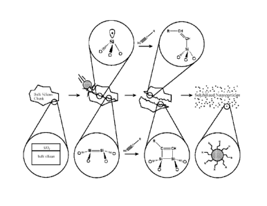
Figure 1 is a schematic diagram that illustrates the overall procedure for
production of
alkyl-passivated silicon nanoparticles, according to the method of the present
invention;
-1 lb-
CA 2724951 2019-11-06
CA 02724951 2010-11-19
WO 2009/011981 PCT/US2008/065534
Figure 2 is a transmission electron microscope (TEM) image obtained of
suspended silicon nanoparticles produced by milling for twenty-four hours in 1-
octyne,
and wherein a number of nanoparticles are indicated by arrows in the image and
can be
seen with sizes ranging from 1-4 nm, with few particles in the range of 5-30
nm;
Figures 3 and 4 are enlargements of the two nanoparticles labeled "B" and "C"
in
Figure 2, with a legend added to indicate scale;
Figure 5 shows a Fourier transform infrared spectrum obtained from silicon
nanoparticles produced by milling for twenty-four hours in 1-octyne, and
wherein for
analysis, the nanoparticles were isolated from the milling solution by rotary
evaporation,
and were dissolved in carbon disulfide;
Figure 6 shows a '3C{ 'H} NMR spectrum;
Figure 7 shows an 1H NMR spectrum, both obtained on prepared alkyl coated
silicon nanoparticles isolated from the milling solvent and dispersed in
methylene
chloride-d;
Figure 8 shows the PL excitation-emission spectrum of alkyl-passivated silicon
nanoparticles produced by milling for 8 hours with 1-octyne as the reactive
media. The
particles exhibit an excitation peak at around 327 nm (not shown in Figure 8),
and an
emission peak at around 405 nm. The emission maximum of 405 nm and the
resulting
Stokes shift of 78 nm is indicative of extremely small crystallite and
particle sizes,
2 0 providing evidence of a large population of nano-sized particles in
solution;
Figure 9 shows size exclusion chromatography of size separated germanium
nanoparticles (selected fractions) in THF solvent and comparison to
polystyrene
standards;
Figure 10 shows a FT-1R spectrum of a specific fraction (Fraction 4) of size
separated germanium nanoparticles with spectral assignments attributed to the
organic
surface layer;
Figure 11 is a transmission electron micrograph of a narrow size distribution
of
germanium nanoparticles from Fraction 6;
Figure 12 is a histogram showing quantitatively the size distribution of
germanium
nanoparticles in Fraction 6;
Figure 13 is a high resolution transmission electron micrograph of fraction 6
-12-
CA 02724951 2010-11-19
WO 2009/011981
PCT/US2008/065534
showing approximately 5nm germanium nanoparticles;
Figure 14 shows optical absorption spectra of different fractions of germanium
nanoparticles;
Figure 15 shows photoluminescence spectra of various fractions of germanium
nanoparticles;
Figure 16 is a low magnification TEM Image of water-soluble germanium
nanoparticles featuring larger nanoparticles;
Figure 17 is a higher magnification image of germanium nanoparticles showing
the size of many of the smaller particles;
1 0 Figure 18 is a high resolution image of a single nanoparticle;
Figure 19 is a UV-Vis absorbance and photoluminescence spectra of germanium
nanoparticles in water;
Figure 20 shows a) FTIR spectrum of passivated silicon nanoparticles produced
by
milling in air b) FTIR spectrum of passivated silicon nanoparticles produced
by milling in
1-octyne for 24 hours c) FTIR spectrum of passivated silicon nanoparticles
produced by
milling in 1-octene for 24 hours d) FTIR spectrum of passivated silicon
nanoparticles
produced by milling in 1-octaldehyde for 24 hours e) FTIR spectrum of
passivated silicon
nanoparticles produced by milling in octanoic acid for 24 hours f) FTIR
spectrum of
passivated silicon nanoparticles produced by milling in 1-octanol for 24
hours;
2 0 Figure 21
shows the resulting structures of silicon nanoparticle surface-bound 1-
octyne, 1-octene, 1-octaldehyde, octanoic acid, and 1-octanol;
Figure 22 shows solubilized passivated nanoparticle concentration against the
passivating molecule chain length;
Figure 23 shows emissions of passivated silicon nanoparticles produced by
milling
in 1-hexyne (0), 1-octyne (A), 1-decyne (0), and 1-dodecyne (N), when excited
under 420
nm light; and
Figure 24 shows emissions of passivated silicon nanoparticles produced by
milling
in 1-hexyne (0), 1-octyne (A), 1-decyne (0), and 1-dodecyne (N), when excited
under 360
nm light.
DETAILED DESCRIPTION OF THE INVENTION
The present invention includes a novel procedure for synthesis of stable alkyl-
or
-13-
CA 02724951 2015-07-17
alkenyl-passivated silicon nanoparticles using high-energy ball milling. The
high energy
ball mill can be a SPEX-type mill. The impact energy for SPEX mills ranges
within the
intervals 0.023 - 0.084 J and 0.069 ¨ 0.252 J for the 4 g and 12 g balls,
respectively. High
energy ball mills like the SPEX models have ball velocities of around 4 m/s,
which
translates to kinetic energy inputs of 0.012 J/hit or power inputs of 0.24 Wig-
ball. The
vials can be nylon vials made from Nylon 6/6 and of the same dimensions as the
commercially available stainless steel vials. The main advantage of this
mechanochemical approach is the simultaneous production of silicon
nanoparticles and
the chemical passivation of the particle surface by alkyl or alkenyl groups
covalently
linked through strong Si-C bonds.
This invention embodies a novel and successful method for the mechanochemical
preparation of stable alkyl- or alkenyl-passivated silicon nanoparticles. This
green
chemistry approach achieves a direct alkylation of the fresh silicon surface
without the
assistance of an unstable hydrogen-terminated intermediate or the use of any
corrosive or
toxic chemicals. The nanoparticles produced are of notably small sizes for a
top-down
comminution method, as particles less than 10 nm have been observed. Such
sizes are not
readily achievable with traditional grinding techniques.
The exhibited blue fluorescence and obvious Stokes shift indicate that the
nanoparticles are largely oxide-free. The nanoparticles prepared by this
method have
.. proven to be thermally-stable and maintain their fluorescence over periods
of months.
This method therefore provides a simple and effective way of producing
alternatively
passivated silicon nanoparticles.
The production of passivated silicon nanoparticles via high energy ball
milling as
described above is traditionally performed in a batch-wise method; i.e., the
reactants are
2 5 loaded in a vial, the process proceeds to completion in the closed
container, and the
products are removed. No material crosses an imaginary boundary surrounding
the
milling vial. The process can be made continuous, or non-batch-wise, by
providing an
input and output stream to the milling vial such that reactants and products
continuously
cross an imaginary boundary surrounding the milling vial.
3 0 After initial start-up, the process achieves steady state and a stream
of passivated
- 14-
CA 02724951 2015-07-17
nanoparticles suspended in the reactive medium is continuously removed from
the milling
vial. The continuous production of functionalized nanoparticles in the
proposed
continuous mechanochemical attrition device can be modeled as a continuous
stirred tank
reactor (CSTR). For the CSTR, reactants flow in (solvent, coarse silicon
chunks), and
products flow out (solubilized silicon nanoparticles, solvent, and partially-
functionalized
silicon particles). The effluent stream would then need to go to a separation
step; e.g., a
continuous centrifuge, such that the partially-reacted particles are separated
out as sludge,
and the solvent with solubilized nanoparticles continues on to purification
steps such as
evaporation or concentration. A filter can be placed in the vial to minimize
the removal of
partially-reacted particles. In this way, most of the micron-scale particles
will remain in
the vial to undergo further comminution and functionalization.
The overall procedure for production of alkyl-passivated silicon nanoparticles
is
illustrated in Figure 1. A milling vial loaded under inert atmosphere with non-
spherical
millimeter-sized (e.g. between about 0.5 microns ¨ 1.0 cm) pieces of
semiconductor-grade
silicon and either a reactive liquid or gaseous medium such as an alkene or
alkyne.
Stainless steel milling balls are added to the vial, which is then sealed and
placed in the
high-energy ball mill. The milling balls are typically one half inch (1.27 cm)
diameter.
Other sizes are available. The diameters could be between about 1 ¨ 50 mm.
High
energy ball milling (HEBM) utilizes ball velocities of around 4 m/s, which
translate to
kinetic energy inputs of 0.012 J/hit, or power inputs of 0.24 Wig-ball.
Measured values of
specific intensity for high energy ball milling have been reported in the
range 0.2 ¨ 1.2
Wig, which is much greater than that found in other types of mills such as
rotary mills, or
other comminutive processes such as grinding. The ongoing impacts and
collisions of the
milling balls (ball-ball and ball-wall impacts) during high energy ball
milling impart a
significant amount of mechanical energy to the system which cause the silicon
pieces to
fracture, thus reducing particle size and creating fresh silicon surface. The
newly-created
surface in high energy ball milling is highly reactive and provides sites for
direct reaction
between the silicon and the reactive medium, preferably and alkene or alkyne.
The alkene
or alkyne reacts with the silicon surface resulting in the formation of a
covalent Si-C
bond.
- 15-
CA 02724951 2010-11-19
WO 2009/011981 PCT/US2008/065534
As high energy ball milling proceeds, particle sizes are reduced into the nano-
domain, and the direct reaction continues with the large amount of resulting
fresh surface.
After high energy ball milling, the vial is allowed to sit undisturbed
allowing any larger
particles to settle leaving the functionalized nanoparticles in solution. This
procedure has
shown to be effective for both alkenes and alkynes. However, a higher
reactivity of
alkynes relative to alkenes over comparable milling times has shown that
alkynes provide
a higher yield of solubilized nanoparticles.
After sufficient milling, two primary phases are formed: the liquid
hydrocarbon
phase that now contains functionalized and solublized nanoparticles, and a
"sediment"
phase that contains a variety of particles, including partially-functionalized
and/or
partially-comminuted particles. In the liquid hydrocarbon phase, the solvent
can be easily
removed, leaving a distribution of functionalized nanoparticles.
Figure 2 is a transmission electron microscope (TEM) image obtained of
suspended silicon nanoparticles produced by milling for 24 hours in 1-octyne.
A number
of nanoparticles can be seen with sizes ranging from 1-4 nm, with few
particles in the
range of 5 to 30 nm. The high-resolution TEM images in Figures 3 and 4 show
individual
single-crystal silicon particles with diameters of approximately 6 nm and 9
nm,
respectively. However, the majority of nanoparticles in Figure 2 are even
smaller than
this, demonstrating that nanoparticles are produced of notably small size for
such a top-
down method. Energy dispersive x-ray spectroscopy (EDS) spectra obtained in
the
nanoparticles in Figures 3 and 4 exhibit distinct peaks at 1.8 keV, confirming
particle
compositions as being silicon. In addition, EDS spectra displayed a lack of
peak at 0.5
keV, indicating particles as being largely oxide-free.
Figure 5 shows a Fourier transform infrared (FTIR) spectrum obtained on
silicon
nanoparticles produced by milling for 24 hours in 1-octyne. For analysis, the
nanoparticles were isolated from the milling solution by rotary evaporation,
and were
dissolved in carbon disulfide. Carbon disulfide was chosen as the solvent such
that its
absorption peaks spectrum would not interfere with those of the nanoparticles'
spectrum.
The infrared spectrum shows clear evidence of an organic layer, as noted by
the strong C-
H stretching bands in the 2800-3000 cm-1, as well as C-H vibrational modes at
1374 cm-1
and 717 cm-1. The pronounced peaks and ¨1257 cm-1, ¨806 cm-1, and ¨796 cm-1
-16-
CA 02724951 2010-11-19
WO 2009/011981 PCT/US2008/065534
correspond to Si-C bonds, indicating that the 1-octyne is indeed bound
covalently to the
surface of the particle.
Nuclear magnetic resonance spectroscopy (NMR) was used to provide further
evidence of a covalently linked surface layer. Figure 6 shows a l'C {1H } NMR
spectrum
and Figure 7 shows an 1H NMR spectrum, both obtained on prepared alkyl coated
silicon
nanoparticles isolated from the milling solvent and dispersed in methylene
chloride-d.
The assignment of CH multiplicities was determined by use of the multipulse
distortionless enhancement by polarization (DEPT) sequence in a separate
experiment.
The 13C spectrum of the nanoparticles clearly shows a uniformity of chemical
environment for the alkyl chain, exhibiting a single methyl resonance and a
distinct
number of methylene chain carbons. Furthermore, three resonance peaks appear
in the
olefinic region of the spectrum at 125, 129, and 142 ppm. The olefinic CH
carbons at 125
and 129 ppm and the quartenary carbon at 142 ppm suggest the formation of a
silicon
surface bond disilacyclobutene structure, resulting from the [2+2]
cycloaddition of the
alkyne to silicon dimer pairs at the surface. The 1H NMR spectrum definitively
shows
alkyl resonances over the 0.5 to 2.5 ppm range due to the alkyl chain, as well
as a singlet
and AB quarter in the vinyl region of this spectrum. While the vinyl singlet
supports the
aforementioned disilaclobutene structure, the AB quartet implies the formation
of a
second bonding structure, in which the alkyl forms a surface bound linear
structure due to
2 0 hydrogen abstraction initiated by a silicon surface radical.
The optical properties of the alkyl-passivated silicon nanoparticles were
investigated at room temperature. Figure 8 shows the PL excitation-emission
spectrum of
alkyl-passivated silicon nanoparticles produced by milling for 8 hours with 1-
octyne as
the reactive media. The particles exhibit an excitation peak at around 327 nm,
and an
emission peak at around 405 nm. The emission maximum of 405 nm and the
resulting
Stokes shift of 78 nm is indicative of extremely small crystallite and
particle sizes,
providing evidence of a large population of nano-sized particles in solution.
Furthermore,
the silicon nanoparticles have shown to be thermally stable, maintaining their
PL for
months after preparation. The quantum yield of the particles has been shown to
be 60
percent.
Synthesis and Size Separation of Germanium Nanoparticles
-17-
CA 02724951 2010-11-19
WO 2009/011981 PCT/US2008/065534
Production of Germanium Nanoparticles:
0.75 g of millimeter sized pieces of germanium of 99.999 % purity obtained
from
Sigma-Aldrich were placed in a stainless steel milling vial along with two
stainless steel
milling balls, each with a diameter of 1.2 cm and weighing approximately 8.1
g. In a
nitrogen-filled glovebox, the vial was loaded, filled with approximately 20 mL
of
trimethylsilylacetylene (?98 % purity), and then tightly sealed. After
charging and
sealing, the milling vial was placed in a SPEX 8000-D Dual Mixer/Mill, and
high energy
ball milling was performed. After 24 hours of milling, the reaction mixture
was
centrifuged to remove larger particles. The supernatant liquid contains a
solution of
TMSA pas sivated germanium nanoparticles. A small amount of methylene chloride
was
used to further extract soluble particles from the milling residue. All
solvent was removed
by rotary-evaporation from the combined liquid extracts to yield a dry
nanoparticle
product. This nanoparticle product may be redispersed in many organic solvents
including
methylene chloride and hexane.
Characterization:
The crude nanoparticle solution contains different sizes of nanoparticles. The
size
separation of nanoparticles was done by gel permeation chromatography (GPC). A
small
amount of concentrated nanoparticle extract was placed on a gravity column
consisting of
200 mesh Bio-Beads S-X1, (Bio-Rad). The nanoparticles were size separated
using
2 0 methylene chloride as an elution solvent. Separate fractions (1.5 ml)
were collected and
used for characterization. For this example, 12 different fractions were
collected with the
earlier fractions containing the larger nanoparticles and the later fractions
containing the
smaller nanoparticles.
FTIR spectra were obtained at 1 cm-1 resolution with 1000 scans using a Bruker
IFS-55 spectrometer. TEM images were taken with a JEOL 2011 TEM using an
accelerating voltage of 200 kV. EDS data were obtained in the TEM using an
Oxford Inca
attachment, using a 3 nm beam spot. NMR spectra were obtained on a Bruker
Avance 300
MHz high resolution NMR spectrometer. The excitation-emission spectra and
photoluminescence data from the nanoparticles were obtained using a Varian
Cary
Eclipse spectrofluorimeter. Particles were dissolved in spectral grade hexane,
and UV-
Visible absorbance peaks obtained on a Cary 50 spectrophotometer provided
reference
-18-
CA 02724951 2010-11-19
WO 2009/011981 PCT/US2008/065534
peaks for the initial excitation wavelengths used during PL analysis.
Figure 9 shows size exclusion chromatography of size separated germanium
nanoparticles (Fractions 1, 3-8, and 11) in THF solvent and comparison to
polystyrene
standards. The sharp peak at approximately 500 amu corresponds to a molecular
side-
product. Most nanoparticles range between 1500 ¨ 70,000 amu. Figure 10 shows a
FT-IR
spectrum of a specific fraction (Fraction 4) of size separated germanium
nanoparticles
with spectral assignments attributed to the organic surface layer. Figure 11
is a
transmission electron micrograph of a narrow size distribution of germanium
nanoparticles from Fraction 6. Figure 12 is a histogram showing quantitatively
the size
distribution of germanium nanoparticles in Fraction 6. The average diameter of
the
nanoparticles is 4.9 nm. Figure 13 is a high resolution transmission electron
micrograph
of fraction 6 showing approximately 5nm germanium nanoparticles. The lattice
fringes
are clearly visible on the particles indicating that they are single crystal.
Figure 14 shows
optical absorption spectra of different fractions of germanium nanoparticles.
Early
fractions (larger particles) show a more pronounced tailing to longer
wavelengths. Figure
15 shows photoluminescence spectra of various fractions of germanium
nanoparticles.
Later fractions (smaller particles) show higher energy (shorter wavelength)
luminescence
in accordance to quantum size effects.
Synthesis of Water Soluble Germanium Nanoparticles
Production of Germanium Nanoparticles:
0.75 g of millimeter sized pieces of germanium of 99.999 % purity obtained
from
Sigma-Aldrich were placed in a stainless steel milling vial along with two
stainless steel
milling balls, each with a diameter of 1.2 cm and weighing approximately 8.1
g. In a
nitrogen-filled glovebox, the stainless steel milling vial was then filled
with
approximately 20 mL of 3-dimethylamino-1-propyne (Sigma-Aldrich, 98% purity),
and
then tightly sealed. The milling vial was then placed in a SPEX 8000-D Dual
Mixer/Mill,
and high-energy ball milling was performed for various lengths of time.
Separation: After 24 hours of milling, the reaction mixture was centrifuged to
remove
larger particles. The solution contained dimethylamino-1-propyne pas sivated
germanium
nanoparticles which are soluble. The 3-dimethylamino- 1-propyne was removed by
rotary-
evaporation to yield solid nanoparticles. Approximately 20m1 of distilled
water was added
-19-
CA 02724951 2015-07-17
to the vial to further dissolve remaining nanoparticles from the residue. The
water was
removed from this fraction by rotary-evaporation to obtain a second batch of
dry
nanoparticle product. This nanoparticle product is soluble in water, methanol
or other
polar solvents and can be redispersed in those solvents for characterization.
Characterization- FTIR spectra were obtained at 1 cm-I resolution with 1000
scans using a Bruker IFS-55 spectrometer. TEM images were taken with a JEOL
2011
TEM using an accelerating voltage of 200 kV. EDS data were obtained in the TEM
using
an Oxford Inca attachment, using a 3 nm beam spot. NMR spectra were obtained
on a
Bruker Avance 300 MHz high resolution NMR spectrometer. The excitation-
emission
spectra and photoluminescence data from the nanoparticles were obtained using
a Varian
Cary Eclipse spectrofluorimeter. Particles were dissolved in distilled water,
and UV-
Visible absorbance peaks obtained on a Cary 50 spectrophotometer provided
reference
peaks for the initial excitation wavelengths used during PL analysis.
Figure 16 is a low magnification TEM Image of water-soluble germanium
.. nanoparticles featuring larger nanoparticles. Figure 17 is a higher
magnification image of
germanium nanoparticles showing the size of many of the smaller particles.
Figure 18 is a
high resolution image of a single nanoparticle. The lattice fringes of this
particle indicate
that it is single crystal. Figure 19 is a UV-Vis absorbance and
photoluminescence spectra
of germanium nanoparticles in water.
2 0 Recently, the present inventors published a new method for the
simultaneous
production of silicon nanoparticles and the chemical passivation of the
particle surface by
alkyl/alkenyl groups covalently linked through Si-C bonds (A. S. Heintz, M. J.
Fink, B. S.
Mitchell. Adv. Mater. 2007, 19, 3984). By subjecting chunks of single-crystal
silicon to
high energy ball milling (HEBM) in the presence of a reactive alkyne, the
nanoparticle
2 5 surface underwent a direct reaction, successfully passivating the
surface while the
particles were simultaneously reduced into the nano-domain by repeated
material fracture.
The previously presented method is not limited to alkynes, and is in fact
applicable to
other reactive organics as well. Specifically, aldehydes, carboxylic acids,
alkenes, and
alcohols were investigated by performing the milling process with 1-octene, 1-
3 0 octaldehyde, octanoic acid, and 1-octanol as the respective reactive
organic liquids during
- 20 -
CA 02724951 2010-11-19
WO 2009/011981 PCT/US2008/065534
milling. Because the previously presented work was done with 1-octyne, the 8-
carbon
chain species of each functional group were selected for the purpose of
consistency and
for ease of comparison. The present inventors have subsequently experimented
as well
with other carbon chain species.
As before, a stainless steel milling vial is loaded under inert atmosphere
with
chunks of single-crystal silicon and the reactive organic liquid of choice.
Stainless steel
milling balls are added to the vial, which is then sealed and subjected to
HEBM. Ongoing
ball-ball and ball-wall impacts during milling impart mechanical energy into
the system,
and silicon pieces trapped in these collisions fracture, reducing particle
size and creating
fresh surface. This newly created surface is highly reactive and provides
sites for direct
reaction between the silicon and the reactive organic, resulting in the
formation of
covalent bonds. As HEBM continues, silicon particle sizes are reduced into the
nano-
domain via comminution, and the direct surface reaction continues as fresh
surface is
continually produced via facture. In all cases, regardless of the reactive
media, milling is
preferably performed for a continuous period of 24 hours.
Figure 20 shows a series of Fourier transform infrared (FTIR) spectra obtained
on
silicon nanoparticles produced by milling in 1-octyne (spectrum b), 1-octene
(spectrum c),
1-octaldehyde (spectrum d), octanoic acid (spectrum e), and 1-octanol
(spectrum f). For
the purpose of comparison, a FTIR spectrum obtained on nanoparticles formed by
milling
2 0 in air (spectrum a) without the presence of a reactive medium is
presented. The
nanoparticles formed by milling in air show only one major feature in the
prominent Si-0-
Si peaks from 900-1200 cm-1 range. It is also important to note the lack of
this same peak
in the other five spectra, showing that milling in the presence of these
reactive organics
does serve to protect the nanoparticles from significant ambient air
oxidation. In all five
cases where the nanoparticles were milled in the presence of a reactive
organic liquid, the
infrared spectra show clear evidence of an organic layer, as evidenced by the
distinct C-H
stretching bands over the 2800-3000 cm-1 range as well as C-H vibrational
modes at
-4347 cm-1 and ¨717 cm-1. Additionally, the spectra obtained on the
nanoparticles
produced in octaldehyde, octanoic acid, and octanol also display ¨OH
stretching over the
3200-3500 cm-1 range, which is thought to be due to oxygen insertion into
surface Si-H
bonds upon exposure to air. The small aldehyde peaks observed in the
octaldehyde and
-21-
CA 02724951 2010-11-19
WO 2009/011981
PCT/US2008/065534
octanoic acid nanoparticle spectra are likely due to residual solvent
molecules.
Table 1 lists photoluminescence (PL) data obtained on silicon nanoparticles
produced by milling in the various organic solvents for 24 hours. Silicon
nanoparticles
produced by milling in 1-octene exhibit the highest intensity emission at -
396 nm when
.. excited with 320 nm light. The nanoparticles produced by milling in 1-
octaldehyde
displayed the highest intensity emission at -518 nm when excited with 440 nm
light.
Similarly, silicon nanoparticles produced by milling with octanoic acid had
the highest
intensity emission at -522 nm when excited with 440 nm light. The highest
intensity
emission observed from nanoparticles produced by milling in 1-octanol was in
the bottom
of the visible region at -406 nm when excited with 290 nm light. The PL
properties of
silicon nanoparticles produced in 1-octyne are listed for comparison purposes.
Table 1: PL data obtained on luminescent silicon nanoparticles produced by
milling
in various organic solvents for 24 hours
Excitation wavelength of Wavelength of
Passivating Molecule
Intensity of maxiumum
maximum observed maximum observed
Functional Group emission (au.)
emission intensity (nm) emission (nm)
1-octyne 360 -435 ¨210
1-octene 320 --394 ¨72
1-octaldehyde 440 --522 ¨48
octanoic acid 440 ¨ 518 ¨ 21
1-octanol 290 ¨ 406 ¨12
Reactive sites on bare unreacted silicon are well characterized on
reconstructed
silicon surfaces under ultra high vacuum conditions. Rolls of reactive Si=Si
dimers and
surface radicals are thought to be the pathway through which the direct
reactions occur.
2 0 As such, it is possible to determine the structures of the surface
bound organic monolayer.
Using 13C and 11-1 nuclear magnetic resonance (NMR) spectroscopy and the
series of
multipulse DEPT tests, the resulting structures of nanoparticle surface bound
1-octene, 1-
-22-
CA 02724951 2010-11-19
WO 2009/011981
PCT/US2008/065534
octaldehyde, octanoic acid, and 1-octanol were characterized, and are
summarized in
figure 21. For comparison purposes, the previously deduced surface-bound
structure for
1-octyne is also shown.
The present inventors have demonstrated herein that their previously reported
method for the simultaneous production and passivation of silicon
nanoparticles is not
limited merely to alkynes, but in fact is also effective with alkenes,
aldehydes, carboxylic
acids, and alcohols. Nanoparticles produced in the presence of the discussed
reactive
organic liquids have shown to fluoresce under UV light, indicating both
sufficient
reduction in size and successful surface passivation with the reactive
molecule.
Establishing this one-step direct reaction method as being flexible to various
functionalities serves to increase its potential applications.
Experimental
Production of Silicon Nanoparticles: 1.0 g of silicon pieces of 99.95% purity
obtained
from Sigma-Aldrich were placed in a stainless steel milling vial along with
two stainless
steel milling balls, each with a diameter of 1.2 cm and weighing approximately
8.1 g. In a
glovebox under nitrogen atmosphere, the vial was loaded, filled with
approximately 25
mL of the desired liquid media, and then tightly sealed. For reactive media, 1-
octanol >
99% purity, octyl aldehyde > 99% purity, and octanoic acid? 98% purity were
all
obtained from Sigma-Aldrich. After charging and sealing, the milling vial was
placed in a
SPEX 8000-D Dual Mixer/Mill, and HEBM was performed over various lengths of
time.
Characterization: FT1R spectra were obtained at 1 cm 1 resolution with 1000
scans using
a Bruker IFS-55 spectrometer. For FT1R For analysis, the nanoparticles were
placed in a
vacuum oven for solvent removal, and were re-dissolved in carbon disulfide
then placed
on a salt plate where the carbon disulfide was allowed to evaporate. The
excitation-
emission spectra and photoluminescence data from the nanoparticles were
obtained using
a Varian Cary Eclipse spectrofluorimeter. Particles were dissolved in heptane,
and UV-
Visible absorbance peaks obtained on a Cary 50 spectrophotometer provided
reference
peaks for the initial excitation wavelengths used during PL analysis.
Nanoparticle Solubility
One of the main advantages of the developed production method is that the
passivated silicon nanoparticles become solubilized in the liquid milling
medium during
-23-
CA 02724951 2010-11-19
WO 2009/011981 PCT/US2008/065534
milling. This allows for easy collection, and facilitates an initial
separation of the
passivated nanoparticles by size via sedimentation.
Nanoparticle Solubilty vs Passivating Molecule Chain Length
It is well known that for organic molecules, longer chain lengths will
generally
correspond to increasing intermolecular forces. This phenomenon can be
observed
through physical properties such a the boiling point of organic liquids; n-
dodecane (b.p.
216.2 C) boils at a higher temperature than does n-decane (b.p. 216.2 C),
which boils at
a higher temperature than n-octane (b.p. 216.2 C), which in turn boils higher
than n-
hexane (b.p. 216.2 C), and so on. Intermolecular van der Waals forces are
determined,
1 0 chiefly, by the number of electrons around the molecule and by the
surface area of the
molecule. Longer (and thus larger) molecules will therefore be subject to
greater attractive
intermolecular forces than will shorter molecules of the same species.
It follows then that the chain length of the passivating molecule should have
an
effect on the solubility of passivated silicon nanoparticles within the
milling solution. By
increasing the chain length of the passivating molecule, the net
intermolecular attractive
force between the nanoparticle and the liquid will increase; essentially, the
nanoparticle
becomes more 'solvent-like' as the passivating molecules become larger. The
attachment
of larger passivating molecules to the nanoparticle surface should allow for
the
solubilization of larger nanoparticles.
2 0 Figure 22 shows the mass concentration in the milling solution of
passivated
silicon nanoparticles formed by milling in the presence of alkynes of carbon
chain lengths
of 6, 8, 10, and 12. As the chain length of the reactive liquid molecule
increases, the
concentration of nanoparticles in solution increases as well. Table 2 lists
the process
yields for passivated silicon nanoparticles formed by milling in the presence
of alkynes of
carbon chain lengths of 6, 8, 10, and 12. Yet again, there is an observed
increase in the
amount of nanoparticles that remain solubilized. Indeed, as the chain length
of the
passivating molecule is increased, a greater mass of silicon nanoparticles
becomes
solubilized in the liquid medium.
Table 2: Process yields of passivated silicon nanoparticles produced by
milling in
alkynes of various chain lengths.
-24-
CA 02724951 2010-11-19
WO 2009/011981 PCT/US2008/065534
Chain Length % Yield
1-Hexyne 6 4.10
1-Octyne 8 4.59
1-Decyne 10 4.96
1-Dodecyne 12 5.24
¨/ g starting Silicon and 20 mL reactive liquid
However, the concentration of nanoparticles within the milling solution as
presented above only goes to show a greater overall mass of the solubilized
nanoparticles,
and speaks nothing of their size. The relation between the size of the
solubilized
nanoparticles and passivating molecule chain length can be achieved through a
comparison of their optical properties. Recall that the bandgap of a silicon
nanoparticle is
size-dependent; smaller silicon nanoparticles have larger bandgaps, and will
thus
luminesce at higher energies. Figure 23 shows the emissions of silicon
nanoparticle
passivated with alkyl molecules of different chain lengths when excited at 420
nm. For
ease of comparison in peak location, the emissions have been normalized to
unity. As the
length of the passivating molecule is increased, there is an observed red-
shift in the
emission maximum. As the red-shift denotes an overall decrease in emission
energy, this
supports the presence of a greater average particle size in the samples with
the longer
chain length. Figure 24 shows the emissions of silicon nanoparticle passivated
with alkyl
molecules of different chain lengths when excited at 360 nm, again normalized
to unity.
Although narrower emissions are observed due to excitation of the smaller
populations, in
similar fashion to before a red-shift is observed with increasing passivating
molecule
chain length.
Chain length variations in the passivating molecule have been shown to affect
the
2 0 size of the passivated silicon nanoparticles that become solubilized in
the liquid medium
during milling. The attachment of longer chains to the nanoparticle surface
results in the
solubilization of larger passivated silicon nanoparticles, and conversely, the
attachment of
shorter chains results in a narrower size distribution. This allows for a
certain degree of
process tuning, as a limited size selection can be performed by simply
altering the reactive
organic used during milling.
In one embodiment of the invention, a semiconductor material, such as silicon
or
-25-
CA 02724951 2010-11-19
WO 2009/011981 PCT/US2008/065534
germanium, is altered from an indirect band gap semiconductor to a direct band
gap
semiconductor through high energy ball milling.
In another embodiment of the invention, the reactive medium includes
polyfunctionalized nanoparticles that are further reactive in specialized
conditions.
In another embodiment of the invention, the high energy ball milling apparatus
takes the form of a fluidized bed in which the reactive medium carries the
silicon or other
material to be comminuted into the fluid bed and in doing so provides momentum
to the
milling balls, causing them to collide. The passivation process proceeds as
previously
described, but the nanoparticles are canied out of the fluidized bed in the
spent reactive
medium.
In another embodiment of the invention, the milling balls are replaced by
impactors, which traverse back and forth in an enclosed preferably polymeric
vial. The
silicon (or other material) fractures in the presence of the reactive medium
as previously
described, except that collisions are between the impactor and the end surface
of the vial.
These impactors can be cylindrical and have dimensions of 1 cm in diameter by
3 cm long
for example, and be made of any magnetic material such as steel (as the
impactors are
preferably agitated with electromagnets (the impactors are preferably magnetic
because
the preferred cryogenic mill (6750 freezer mill produced by SPEX) uses a
magnet to make
the impactor move back and forth, whereas the SPEX high energy ball mill uses
a
2 0 mechanical motor and swing arm to get the vial moving, the cryomill
instead uses
magnets to move the impactor)).
In another embodiment of the invention, the passivated silicon nanoparticles
are
formed in a batch-wise operation.
In another embodiment of the invention, the passivated silicon nanoparticles
are
formed and removed from the high energy ball milling apparatus in a continuous
manner.
All measurements disclosed herein are at standard temperature and pressure, at
sea
level on Earth, unless indicated otherwise. All materials used or intended to
be used in a
human being are biocompatible, unless indicated otherwise.
The foregoing embodiments are presented by way of example only; the scope of
the present invention is to be limited only by the following claims.
-26-