Note: Descriptions are shown in the official language in which they were submitted.
CA 02725186 2010-11-22
WO 2009/142656
PCT/US2008/079016
METAL-CONTAINING TRANSACTION CARD AND METHOD
OF MAKING THE SAME
Field of Invention
The invention generally includes metal-containing transaction cards useful for
the
purchase of goods and/or services and methods of making the same. The cards
may include
other features such as a microchip (e.g., smart card), an antenna and a
backplate.
Background Of The Invention
The proliferation of transaction cards, which allow the cardholder to pay with
credit
rather than cash, started in the United States in the early 1950s. Initial
transaction cards
= were typically restricted to select restaurants and hotels and were often
limited to an
exclusive class of individuals. Since the introduction of plastic credit
cards, the use of
transaction cards have rapidly proliferated from the United States, to Europe,
and then to the
rest of the world. Transaction cards are not only information carriers, but
also typically
allow a consumer to pay for goods and services without the need to constantly
possess cash,
or if a consumer needs cash, transaction cards allow access to funds through
an automatic
teller machine (ATM). Transaction cards also reduce the exposure to the risk
of cash loss
through theft and reduce the need for currency exchanges when traveling to
various foreign
countries. Due to the advantages of transaction cards, hundreds of millions of
cards are now
produced and issued annually, thereby resulting in a need for companies to
differentiate their
cards from competitor's cards.
Initially, the transaction cards often included the issuer's name, the
cardholder's
name, the card number, and the expiration date embossed onto the card. The
cards also
usually included a signature field on the back of the card for the cardholder
to provide a
signature to protect against forgery and tampering. Thus, the cards served as
devices to
provide data to merchants and the security associated with the card was the
comparison of
the cardholder's signature on the card to the cardholder's signature on a
receipt along with
the embossed cardholder's name on the card.
Due to the popularity of transaction cards, numerous companies, banks,
airlines,
trade groups, sporting teams, clubs and other organizations have developed
their own
transaction cards. As such, many companies continually attempt to
differentiate their
transaction cards and increase market share not only by offering more
attractive financing
rates and low initiation fees, but also by offering unique, aesthetically
pleasing features on
- 1 -
CA 02725186 2010-11-22
WO 2009/142656
PCT/US2008/079016
the transaction cards. As such, many transaction cards include not only
demographic and
account information, but the transaction cards also include graphic images,
designs,
photographs and security features. A recent security feature is the
incorporation of a
diffraction grating, or holographic image, into the transaction card which
appears to be
three-dimensional. Holographic images restrict the ability to fraudulently
copy or reproduce
transaction cards because of the need for extremely complex systems and
apparatus for
producing holograms.
Administrative and security issues, such as charges, credits, merchant
settlement,
fraud, reimbursements, etc., have increased due to the increasing use of
transaction cards.
Thus, the transaction card industry started to develop more sophisticated
transaction cards
which allowed the electronic reading, transmission, and authorization of
transaction card
data for a variety of industries. For example, magnetic stripe cards, optical
cards, smart
cards, calling cards, and supersmart cards have been developed to meet the
market demand
for expanded features, functionality, and security. In addition to the visual
data, the
incorporation of a magnetic stripe on the back of a transaction card allows
digitized data to
be stored in machine readable form. As such, magnetic stripe readers are used
in
conjunction with magnetic stripe cards to communicate purchase data received
from a cash
register device on-line to a host computer along with the transmission of data
stored in the
magnetic stripe, such as account information and expiration date.
Due to the susceptibility of the magnetic stripe to tampering, the lack of
confidentiality of the information within the magnetic stripe and the problems
associated
with the transmission of data to a host computer, integrated circuits were
developed which
may be incorporated into transaction cards. These integrated circuit (IC)
cards, known as
smart cards, proved to be very reliable in a variety of industries due to
their advanced
security and flexibility for future applications. However, even integrated
circuit cards are
susceptible to counterfeiting.
As magnetic stripe cards and smart cards developed, the market demanded
international standards for the cards. The card's physical dimensions,
features and
embossing area were standardized under the International Standards
Organization ("ISO"),
ISO 7810 and ISO 7811. The issuer's identification, the location of particular
compounds,
coding requirements, and recording techniques were standardized in ISO 7812
and ISO
7813, while chip card standards were established in ISO 7813. For example, ISO
7811
defines the standards for the magnetic stripe which is a 0.5 inch stripe
located either in the
- 2 -
CA 02725186 2010-11-22
WO 2009/142656
PCT/US2008/079016
front or rear surface of the card and which is divided into three
longitudinally parallel tracks.
The first and second tracks hold read-only information with room for 79
alphanumeric
characters and 40 numeric characters, respectively. The third track is
reserved for financial
transactions and includes enciphered versions of the user's personal
identification number,
country code, currency units, amount authorized per cycle, subsidiary
accounts, and
restrictions.
More information regarding the features and specifications of transaction
cards can
be found in, for example, Smart Cards by Jose Luis Zoreda and Jose Manuel
Oton, 1994;
Smart Card Handbook by W. Rankl and W. Effing, 1997, and the various ISO
standards for
transaction cards available from ANSI (American National Standards Institute),
11 West
42nd Street, New York, NY 10036.
The incorporation of machine-readable components onto transactions cards
encouraged the proliferation of devices to simplify transactions by
automatically reading
from and/or writing onto transaction cards. Such devices include, for example,
bar code
scanners, magnetic stripe readers, point of sale terminals (POS), automated
teller machines
(ATM) and card-key devices. With respect to ATMs, the total number of ATM
devices
shipped in 1999 was 179,274 (based on Nilson Reports data) including the ATMs
shipped
by the top ATM manufacturers, namely NCR (138-18 231st Street, Laurelton, New
York
11413), Diebold (5995 Mayfair, North Canton, Ohio 44720-8077), Fujitsu (11085
N. Torrey
Pines Road, La Jolla, California 92037), Omron (Japan), OKI (Japan) and
Triton.
Typical transaction cards are made from thermoplastic materials, such as
polyvinyl
chloride (PVC) and polyethylene terephthalate (PET). However, these
transaction cards are
susceptible to being damaged or destroyed if exposed to damaging environments.
For
example, transaction cards may be damaged if left exposed to the elements for
an extended
period of time. Moisture and/or sunlight may break down the chemical bonds
within the
polymers of typical transaction cards, such that transaction cards left
exposed to moisture
and sunlight may become warped, cracked and unusable. In addition,
thermoplastic
transaction cards may be easily bent or may be broken or cut, thereby damaging
the
transaction card and rendering it unusable.
A need, therefore, exists for a transaction card that has both strength and
durability.
Moreover, a need exists for a transaction card that withstands exposure to the
elements, such
as moisture or sunlight. A need further exists for a transaction card that may
incorporate the
features noted above, such as holograms, signature panels, magnetic stripes,
microchips, and
- 3 -
CA 02725186 2013-11-08
the like, such that is has both strength and durability. In addition, a need
exists for a
transaction card that overcomes the problems noted above.
Summary of the Invention
The present invention relates to a metal-containing transaction card and a
method of
making the same. The transaction card may have a magnetic stripe, an embedded
microchip, a signature panel, a holographic image, or any other feature
typically contained
on or within the transaction card. The transaction card of the present
invention may have at
least one layer of metal. The transaction card of the present invention may
have at least one
layer of titanium or stainless steel.
A transaction card and a method of making the same are provided whereby the
transaction card may have at least one layer of metal. The at least one layer
of metal may
provide durability and strength to the transaction card. The one layer of
metal may be any
metal able to be utilized as a transaction card or incorporated into or within
a transaction
card. The at least one layer of metal may be titanium, stainless steel or
aluminum.
Further, a transaction card having at least one layer of metal is provided
whereby the
transaction card may be of a standard size, i.e., compliant with the
International Standards
Organization (ISO) for transaction cards.
In addition, a transaction card having at least one layer of metal may further
have
other layers that include one or more polymeric materials or other metal
material, such as
aluminum and the like.
Still further, a metal-containing transaction card is provided having features
typically
contained on or in transaction cards, such as magnetic stripes, embedded
microchips,
signature panels, holographic images, and the like. Moreover, the metal-
containing
transaction card may be printed with indicia, such as via screen-printing or a
laser-etching
process to uniquely identify the transaction card and/or the issuer of the
transaction card or
any other information.
According to an aspect of the present invention there is provided a method
of making a transaction card comprising:
cutting a first sheet of metal to create a card body;
cutting a second sheet of metal to create a back panel;
applying an adhesive to said back panel;
bonding said back panel to said card body; and
milling a pocket into said card body.
According to another aspect of the present invention there is provided a
transaction card comprising:
- 4 -
CA 02725186 2013-11-08
a card body having a first surface and a second surface that is continuous
over the entire area of said transaction card;
a back panel, wherein said back panel is bonded to said second surface;
a pocket disposed in said first surface; and
a microchip disposed in said pocket.
Additional features and advantages of the present invention are described in,
and will
be apparent from, the detailed description of the presently preferred
embodiments and from
the drawings.
Brief Description of the Drawings
FIG. 1A Illustrates a plan view of a front face of a metal-containing
transaction card;
- 4a -
CA 02725186 2010-11-22
WO 2009/142656
PCT/US2008/079016
FIG. 1B illustrates a plan view of a back face of a metal-containing
transaction card;
FIG. 2A illustrates a cross-sectional view of a metal-containing transaction
card
along line II-II of FIG. 1B;
FIG. 2B illustrates a cross-sectional view of an alternate embodiment of a
transaction
card along line II-II of FIG. 1B;
FIG. 2C illustrates a cross-sectional view of another alternate embodiment of
a
transaction card along line II-II of FIG. 1B;
FIG. 2D illustrates a cross-sectional view of a still further alternate
embodiment of a
transaction card along line II-II of FIG. 1B;
FIG. 2E illustrates a cross-sectional view of another alternate embodiment of
a
transaction card along line II-II of FIG. 1B;
FIG. 3 illustrates a flow chart showing a method of making metal-containing
transaction cards;
FIG. 4 illustrates a flow chart showing an alternate method of making titanium
transaction cards;
FIG. 5 illustrates another flow chart showing an alternate method of titanium
transaction cards;
FIG. 6 illustrates an alternate flow chart showing a still further alternate
method of
making titanium transaction cards;
FIG. 7 illustrates a still further alternate flow chart showing an alternate
method of
making titanium transaction cards with embossed characters, a magnetic stripe
and a
signature panel;
FIG. 8 illustrates a plan view of a titanium card made by the methods of
making the
titanium transaction cards;
FIG. 9 illustrates a plan view of an inset fill panel made during the methods
of
making the titanium transaction cards;
FIG. 10 illustrates a plan view of an embossed titanium card with adhesive
disposed
in the pockets;
FIG. 11 illustrates a plan view of a titanium card having a fill panel
disposed within a
pocket and a magnetic stripe and signature panel disposed in the other
pockets;
FIG. 12 illustrates a cross-sectional view of the titanium card having the
fill panel
disposed within the pocket and a magnetic stripe and signature panel disposed
in other
pockets;
- 5 -
CA 02725186 2010-11-22
WO 2009/142656
PCT/US2008/079016
FIGs 13A and 13B illustrate a method of making a metal transaction card;
FIGs 14A-14C illustrate a metal transaction card.
Detailed Description
Metal-containing transaction cards and methods of making the same are
provided.
The transaction cards may be standard-sized (i.e., about 3 3/8 inches by about
2 1/4 inches) or
any other size yet still usable as a transaction card. Moreover, the
transaction card may have
a magnetic stripe, an embedded microchip, a signature panel, a holographic
image, or any
other feature typically contained on or within a transaction card. The
transaction cards may
have at least one layer of metal, including titanium or stainless steel.
Referring now to the drawings, wherein like numerals refer to like parts, FIG.
1
illustrates a plan view of a metal-containing transaction card 1 having a
front face 10. The
transaction card 1 may be composed of at least one layer of metal that has
been flattened
into a card shape. Typically metal can be rolled into a sheet. The sheet can
then be cut to
form individual transaction cards.
Any metal may be utilized as the layer or layers of the transaction cards
described
herein. Specifically, the metals may include titanium, stainless steel, or
aluminum, although
any other metal is contemplated by the present invention. The transaction card
of the
present invention may comprise titanium.
On the front surface 10 of the transaction card 1 may be indicia, such as
images,
graphics, words, or other symbols, that may be printed on the front surface 10
using
conventional printing techniques. Alternatively, the indicia may be laser-
etched. A typical
laser-etching device for laser-etching metal, such as titanium or stainless
steel, is done by a
laser from Virtek Vision International, Inc. Lasers can provide marking of
metals such as
titanium, stainless steel or aluminum of depths of up to 0.100 inches and as
low as about
0.003 inches. A pattern may be laser marked onto the front face 10 (or the
rear surface 20,
as described below and illustrated by FIG. 1B).
In addition, the laser-etching of the metal layer, typically titanium, may
provide the
transaction card 1 with a plurality of colors on one or both of the faces of
the card 1.
Specifically, the energy utilized to laser-etch the metal may allow the metal
to recrystallize
in such a way as to be viewable by an individual as being of a specific color
or colors.
- 6 -
CA 02725186 2010-11-22
WO 2009/142656
PCT/US2008/079016
In an alternative embodiment, one or both surfaces of the transaction card 1
may be
anodized using conventional anodizing methods, thereby providing one or both
surfaces of
the transaction card 1 that may sealed with an oxide layer thereby protecting
the metal and
allowing the surface to be receptive to printing inks or coatings. In
addition, the anodizing
process may provide a color to one or both surfaces of the transaction card 1.
For example,
the anodizing process may comprise treatment of the surface of the metal with
an ionic
solution under an electrical current, which can provide one or both faces of
the transaction
card 1 with a color depending on the voltage of the electricity that is used
to anodize the one
or both faces of the transaction card 1.
A coating may be applied to one or both faces of the transaction card 1. The
coating
may be a silane compound thereby providing the metal in the transaction card 1
resistance to
scratches, damage, fingerprints, and the like. In addition, a dye or ink may
be incorporated
into the silane coating thereby providing the transaction card 1 with a
particular color.
Typically, the silane and the dye are provided across one or both surfaces of
the transaction
card 1. The silane coating may be incorporated with a black dye whereby one or
both
surface of the transaction card 1 will have a black appearance. Of course, any
other colored
coating may be applied to the surface of one or both faces of the transaction
card 1 after one
or both surfaces of the transaction card 1 are anodized, such as acrylic or
polyethylene
terephthalate. In addition, the surface coating may be comprised of a
thermoset polymeric
material, applied to one or both surfaces of the transaction card. The
thermoset material
may be applied to the transaction card 1 by coating one or both surfaces of
the transaction
card 1 with dry powder of the thermoset material, and baking the thermoset
material to melt
the same and set the material on the surface of the transaction card 1. Of
course, the
transaction card 1 may be provided with no colored coating, thereby providing
a metal-
colored transaction card, whereby the natural color of the metal may be
viewable.
FIG. 1B illustrates a rear surface 20 of the transaction card 1 of the present
invention.
Provided on the rear surface 20 may be a magnetic stripe 22 that may be
applied to the rear
surface 20 using conventional methods, such as by stamping the magnetic stripe
to the
transaction card 1. Moreover, a signature panel 24 may be provided as well and
may also be
stamped to the transaction card 1 or applied via any other conventional
method. The
signature panel allows the owner of the transaction card to place his or her
signature on the
transaction card, thereby providing a security feature. In addition, a
microchip may be
embedded into the transaction card of the present invention. Of course, any
other feature
- 7 -
CA 02725186 2010-11-22
WO 2009/142656
PCT/US2008/079016
may be included on the front surface 10 or the rear surface 20 of the
transaction card 1 as
may be apparent to one having ordinary skill in the art.
FIG. 2A illustrates a cross-sectional side view of the transaction card 1
along lines II-
II of FIG. 1B. As illustrated, the transaction card 1 includes at least a
first layer 26 of metal.
Of course, the transaction card 1 may comprise two or more layers of metal
that are adhered
together via heat, pressure, and/or adhesive. The transaction card 1 may
include at least one
layer of titanium or stainless steel. The first layer 26 further includes the
magnetic stripe 22
and the signature panel 24 adhered directly to the first layer 26 of metal.
The total thickness
of the first layer 26 may be about 30 mils, although other thicknesses of the
first layer 26 are
contemplated by the present invention. The layers illustrated in FIGS. 2A-2E
are
exaggerated in thickness to clearly illustrate the structures of the
transaction cards described
herein.
The transaction card 1 may be stamped, embossed or etched to provide texture,
images, alphanumeric characters, or the like. As described above, the front or
rear surfaces
of the transaction card 1 may be printed or laser-etched to provide indicia,
such as graphics,
images, text, or any other indicia. In addition, the surface of the first
layer 26 may be
anodized and/or coated with a coating to protect the surfaces of the metal
and/or to provide
the surface with a color. Moreover, an adhesive (not shown) may be provided
for adhering
the magnetic stripe 22 and the signature panel 24 to the metal of the first
layer 26. Further, a
microchip (not shown) may be embedded into the first layer 26 of metal to
provide smart
card capabilities to the transaction card made therefrom.
FIG. 2B illustrates an alternate embodiment of the present invention of a
cross-
sectional view of the transaction card 1 along line II-II of FIG. 1B. As
illustrated, the
transaction card 1 includes a metal layer 30, and an optional adhesive layer
32 to adhesively
secure the magnetic strip 22 and signature panel 24 to the metal layer 30. The
adhesive
layer 32 may be laminated, coated, or otherwise applied to the metal layer 30.
The total
thickness of the transaction card 1 including the metal layer 30 and the
adhesive layer 32, as
illustrated in FIG. 2B, may be about 30 mils, although other thicknesses are
contemplated in
the present invention. The metal layer 30 may be made of titanium or stainless
steel.
Alternatively, the transaction card does not include an adhesive layer, as
illustrated
in FIG. 2A, and the magnetic stripe 22 and/or signature panel 24, as well as
any other
feature, is applied directly to one or both surfaces of the metal layer 30.
Alternatively, the
- 8 -
CA 02725186 2010-11-22
WO 2009/142656
PCT/US2008/079016
transaction card 1 may have an adhesive layer (not shown) provided on the
front face 10 of
the transaction card 1 for adhering inks or other printing to the metal layer
30.
The transaction card of FIG. 2B may be stamped, embossed or etched to provide
texture, images, graphics, alphanumeric characters or the like to the
transaction card. As
described above, the front or rear surfaces of the transaction card may be
printed or laser-
etched to provide indicia, such as graphics, images, text, or any other
indicia.
FIG. 2C illustrates an alternate embodiment of the present invention of a
cross-
sectional view of a transaction card taken along line II-II of FIG. 1B. In the
embodiment
illustrated in FIG. 2C, the transaction card 1 comprises a core layer 40 of a
substrate, such as
a thermoplastic material of, for example, PVC, PET copolymer, or other
substrate. Further,
the core layer 40 has a layer of metal laminated to one or both sides of the
core layer 40. In
FIG 2C, the core layer 40 has a first metal layer 42 laminated or otherwise
disposed adjacent
to a first surface of the core layer 40 and a second metal layer 44 laminated
or otherwise
disposed adjacent to a second surface of the core layer 40. The core layer 40
may be about
18 mils, while each metal layer 42, 44 may be about 6 mils to provide a
transaction card that
is about 30 mils in total thickness. However, the core layer 40 and metal
layers 42, 44 may
be any thickness. The metal layers 42, 44 may be titanium or stainless steel.
Provided on the second metal layer 44 may be an adhesive 46 laminated or
otherwise
applied thereto for providing adhesion for the magnetic stripe 22, signature
panel 24, or
other feature typically included on a transaction card. Alternatively, an
adhesive layer (not
shown) is provided on the first metal layer 42 for providing adhesion to inks
for printing
purposes, or for any other reason. Alternatively, there is no adhesive layer
between the
magnetic stripe 22, signature panel 24, or other feature typically included on
the transaction
card and the first and/or second metal layers 42, 44.
In addition, the transaction card of FIG. 2C may be stamped, embossed or
etched to
provide texture, images, graphics, alphanumeric characters or the like to the
transaction
card. As described above, the front or rear surfaces of the transaction card
may be printed or
laser-etched to provide indicia, such as graphics, images, text, or any other
indicia.
FIG. 2D illustrates a fourth embodiment of the present invention, whereby the
transaction card 1, illustrated in a cross-sectional view in FIG. 2D,
comprises a first layer 50
of a substrate, such as a thermoplastic material of, for example, PVC or PET
copolymer, and
a second layer 52 of metal laminated or otherwise disposed adjacent to the
first layer 50.
The first layer 50 and the second layer 52 may have thicknesses that sum to
about 30 mils.
- 9 -
CA 02725186 2010-11-22
WO 2009/142656 PCT/US2008/079016
For example, the first layer may be about 18 mils and the second layer (of
metal) may be
about 12 mils. However, the layers may be any other thicknesses. The second
layer 52 of
metal may be titanium or stainless steel.
The first layer 50 may further include an adhesive 54 to provide adhesion to
the =
magnetic stripe 22, the signature panel 24, or to any other feature contained
on the
transaction card 1. Alternatively, no adhesive layer is present.
FIG. 2E illustrates a fifth embodiment of the present invention, whereby the
transaction card 1, illustrated in a cross-sectional view in FIG. 2E,
comprises a first layer 60
of a metal substrate, such as aluminum, or other metal substrate, and a second
layer 62 of a
second metal laminated or otherwise disposed adjacent to the first layer 60.
The second
layer 62 may be titanium or stainless steel, although other metals are
contemplated by the
present invention. As with the transaction cards described above, the first
layer 60 may have
an adhesive layer 64 laminated or otherwise applied thereto for providing
adhesion to the
magnetic stripe 22 and/or the signature panel 24. As with the other embodiment
described
above, the adhesive may be provided on the second layer as well for providing
adhesion to
inks for printing, or for other features typically contained on a transaction
card.
Alternatively, no adhesive layer is present and the magnetic stripe 22 and/or
the signature
panel 24 are adhered directly to the metal substrate 60.
The following embodiments described herein and illustrated in FIGS. 3-12
relate
specifically to transaction cards made from titanium. However, it should be
noted that the
present invention should not be limited as described, but should also include
embodiments
whereby other metals, blends and alloys are utilized.
FIG. 3 illustrates a method 100 of making a metal-containing transaction card
of the
present invention, wherein the metal is titanium. Specifically, the method 100
includes a
first step 102 of preparing the titanium to form into transaction cards.
Specifically a sheet of
titanium may be prepared that is about 30 mils thick. Typically, the titanium
metal is rolled
and flattened to the required thickness. The titanium sheet may comprise
titanium metal that
has little to no magnetic properties, so that the titanium does not interfere
with the magnetic
stripe and/or microchip that may be embedded within the transaction card.
In an anodizing step 104, the titanium sheet is anodized using a conventional
anodizing process. Specifically, the titanium may be disposed in a bath having
ions and an
electrical current therein to anodize one or both of the faces of the sheet of
titanium. As
noted above, anodizing the sheet of titanium can provide one or both faces of
the sheet of
- 10 -
CA 02725186 2010-11-22
WO 2009/142656
PCT/US2008/079016
titanium with a colored surface, depending on the current that is supplied
during the
anodizing process, as is apparent to one having ordinary skill in the art.
Moreover,
anodizing oxidizes the surface of the titanium, thereby sealing and protecting
the titanium.
In a coating step 106, a coating is applied to one or both faces of the sheet
of
titanium to provide one or both faces of the sheet with a color and to further
protect the
titanium. Specifically, the coating may be a silane coating having a dye
contained therein,
wherein the silane is coated as a layer on one or both faces of the
transaction card. The
silane coating may be applied in a waterless solvent or a water-based system.
In addition,
other materials that may be coated to one or both faces of the transaction
card are
polyethylene terephthalate and acrylic, although any other coating may be
utilized to provide
a coating to protect the titanium and, optionally, to provide a color to the
one or both faces
of the transaction card. For example, the coating may be made from a thermoset
material
that may be sprayed onto the one or both surfaces of the transaction card in
powder form.
The transaction card may then be baked, and the powder may melt to the surface
of the
transaction card.
Step 108 illustrates a cutting step whereby the sheet of titanium, which may
have
been anodized and/or coated as described above, may be cut into individual
transaction card
shapes. Common methods of cutting titanium include, but are not limited to,
water jet
cutting, die cutting, laser cutting or plasma cutting. The goal in cutting the
titanium is to
easily and efficiently cut the titanium sheet into transaction card shapes
while avoiding sharp
edges.
After cutting the titanium sheet via step 108, the individual transaction
cards may be
laser-engraved via a laser-engraving step 110. The laser engraving may be done
via
commonly known laser engraving techniques to provide a pattern in one or both
faces of the
transaction card. Moreover, the laser engraving may cut away a coating that
may be
disposed on the one or both faces of the transaction card, thereby providing a
visible pattern.
For example, if a black coating is applied to the titanium sheet via step 106,
the laser beam
may etch a pattern in the black coating to give a pattern that is not black,
but may be metal
colored, or colored in any other way. In addition, the laser beam may melt the
surface of
one or both faces of the transaction card, which may cause the titanium to
recrystallize when
cooled. The recrystallization may produce a variety of colors in the surface
of one or both
faces of the transaction card. The laser engraving step 110 may be
accomplished via a laser,
such as, for example, a YAG laser having a wavelength of about 1064
nanometers. Of
-11-
CA 02725186 2010-11-22
WO 2009/142656 PCT/US2008/079016
course, any other laser may be utilized that provides a pattern, a texture or
a color to the
titanium as may be apparent to one having ordinary skill in the art.
After laser engraving the transaction card, a magnetic stripe and signature
panel of
the transaction card may be applied to the transaction card via step 112.
Typically, the
magnetic stripe and the signature panel are stamped using techniques common in
the art of
making transaction cards. Specifically, the magnetic stripe and signature
panel are applied
to one or both of the surfaces of the transaction card with the use of an
adhesive that may be
applied on one or both surfaces of the transaction card. The adhesive may be
screen-printed
to one or both surfaces of the transaction card, although any other method of
applying the
adhesive is contemplated by the present invention. Most materials require the
use of an
adhesive to adhere to one or both surfaces of the transaction card. However,
certain coatings
may allow the magnetic stripe and the signature panel to be applied without
the use of
adhesives. For example, a coating of thermoplastic, such as a flat black vinyl
thermoplastic,
may be coated onto the card and may allow the magnetic stripe and the
signature panel to be
applied to the transaction card without adhesive. The stamping process may
melt the
thermoplastic material, thereby allowing the thermoplastic material to adhere
the magnetic
stripe and/or the signature panel when cooled and solidified.
After the magnetic stripe and the signature panel have been applied to the
transaction
card, the transaction card may be milled via step 114 to provide a space to
apply an
embedded microchip for a smart card. The milling process may be done in a
similar manner
to conventional plastic transaction cards, but may be accomplished with a
boron nitride or
boron carbide tipped machine or other machine able to mill titanium. In
addition, the
transaction card may be milled via a cryo-milling process, in which the mill
head is cooled
with a stream of liquid nitrogen to ensure that the transaction card and/or
the mill head does
not overheat. Typically, the transaction card may have an area about 20 to
about 25 mils =
deep milled from the transaction card to provide a space for a microchip. The
microchip
may be applied to the milled area of the transaction card, and may stay within
the milled
area due to an adhesive that may be disposed therein.
After milling the transaction card to embed the microchip therein, the
transaction
card may be embossed via an embossing step 116. Specifically, the embossing
may be done
by subjecting the transaction card to a high pressure die that may punch a
character or a
plurality of characters into the surface of the transaction card. The
embossing may be done
to provide information on the surface of the transaction card that may be
readable by an
- 12 -
CA 02725186 2010-11-22
WO 2009/142656
PCT/US2008/079016
individual or a machine. Specifically, an account number or other unique
identifier is
typically embossed on a transaction card. The embossing step 116 may be
accomplished
with an addressograph machine. Of course, other methods of embossing the
transaction card
are contemplated, and the invention should not be limited as herein described.
Finally, the transaction card may be encoded via step 118 via any encoding
steps
commonly used to encode the transaction cards. Specifically, either or both of
the
recordable media, such as the magnetic stripe and/or the microchip, may be
encoded to
provide the transaction card having information contained therein. The
recordable media
may be read via a magnetic stripe reader or a microchip reader, as may be
apparent to one
having ordinary skill in the art.
FIG. 4 illustrates an alternate method 200 of making transaction cards
comprising
titanium. The method 200 comprises a first step 202 of preparing the titanium
by rolling and
flattening the titanium into a sheet to form into transaction cards. The first
step 202 may be
substantially similar to the first step 102 described above with respect to
FIG. 3.
After the titanium sheet is prepared via step 202, the titanium sheet may be
cut in a
cutting step 204, whereby the sheet of titanium may be cut into individual
transaction card
shapes. For example, the titanium sheet may be cut via the methods described
above with
respect to step 108 of FIG. 3.
Once the individual transaction cards have been cut from the titanium sheet,
each
individual transaction card may be tumbled and cleaned to smooth any sharp
edges via a
tumbling and cleaning step 206. It is important to ensure that all of the
edges are smooth.
After the transaction cards have been smoothed and cleaned, each transaction
card may be -
anodized and primed via an anodizing step 208. The anodizing step may be
substantially
similar to the anodizing step 104 as described above with reference to FIG. 3.
After being anodized and primed, each transaction card may be coated and oven
cured via a coating step 210. The coating step 210 may be substantially
similar to the
coating step 106 as described above with reference to FIG. 3. Each side of
each transaction
card may be coated and oven-cured separately in a multi-step process.
After each side of each transaction card is coated and oven-cured, each
transaction
card may be laser engraved via laser engraving step 212, which may be
substantially similar
to the laser-engraving step 110, as described above with reference to FIG. 3.
Once each transaction card is laser engraved, a primer may be applied to one
or both
of the surfaces by screen printing the primer via a priming step 214. The
primer may be
- 13 -
CA 02725186 2010-11-22
WO 2009/142656
PCT/US2008/079016
applied across the entire surface of each transaction card, or may be applied
precisely where
the magnetic stripe and/or signature panels are desired.
After each transaction card is primed, the magnetic stripe and/or signature
panels
may be applied via step 216. The magnetic stripe and/or signature panel may be
applied in a
substantially similar way as described in step 112, described above with
respect to FIG. 3.
After the magnetic stripe and/or signature panels have been applied, each of
the surfaces of
each transaction card may be laser scored via step 218 to provide graphics,
text and
numerals to either or both of the surfaces of each transaction card.
Once each transaction card has been laser scored to provide graphics, text,
numerals
and/or other indicia, a microchip may be disposed within the transaction card
via step 220.
For example, the transaction card may be milled to provide a space in the
transaction card
for an embedded microchip. The disposing of the microchip into the transaction
card via
step 220 may be done in a substantially similar manner as step 114, described
above with
reference to FIG. 3.
Each transaction card may then be embossed via an embossing step 222, which
may
be substantially similar to the embossing step 118, as described above with
reference to FIG.
3. Finally, each transaction card's recordable media, such as the magnetic
stripe and/or the
embedded microchip, may be encoded via an encoding step 224.
In an alternate method 300 of making titanium transaction cards illustrated in
FIG. 5,
sheets of titanium are prepared via step 302. The titanium sheets may be
prepared as
described above in steps 102, 104 with respect to FIGS. 3, 4, respectively.
Specifically
sheets of titanium may be prepared that are about 30 mils thick. In addition,
other sheets of
titanium may be prepared that are about 15 mils thick, that will be cut into
inset fill panels,
as described below. Typically, the titanium metal is rolled and flattened to
the required
thickness. The titanium sheets may comprise titanium metal that has little to
no magnetic
properties, so that the titanium does not interfere with the magnetic stripe
and/or a microchip
that may be embedded within the transaction card.
The 30 mil thick titanium sheets are then cut into individual cards via step
304. At
the same time, the edges of the individual cards may be beveled to create
chamfer edges.
The chamfer edges may be prepared on both surfaces of each individual card on
all four
edges of each titanium card. Alternatively, the chamfer edges may be prepared
on only one
surface of each titanium card, such as on a front surface of each titanium
card. In addition,
at the same time that the chamfer edges are prepared, a pocket may be milled
into each
- 14-
CA 02725186 2010-11-22
WO 2009/142656
PCT/US2008/079016
individual card. The pocket may be milled into a backside of each transaction
card at the
same location on the transaction card where the transaction card is embossed
to provide
characters on the front surface of each transaction card.
Referring now to FIG. 5, the 15 mil thick titanium sheets may then be cut into
individual inset fill panels via step 306. The inset fill panel will fit
within the pocket when
placed therein with a suitable adhesive. When the inset fill panel is disposed
within the
pocket with a suitable adhesive, the inset fill panel forms a smooth surface
on the backside
of the titanium card.
Both the titanium cards and the inset fill panels may then be brushed via step
308 to
provide a nice finish on each transaction card. Typically, the brushing is
done via known
titanium brushing techniques to provide titanium surfaces having a grain
running in the same
direction. The brushing may also create titanium surfaces on each transaction
card having
another pattern.
Both surfaces of each titanium card may be coated via step 310 by physical
vapor
deposition ("PVD") of a coating that may be utilized to both protect the
titanium surfaces
and provide a distinctive appearance. The coating may be titanium
carbonitride, which,
when vapor deposited on the surfaces of each titanium card, provides an even
and
substantially black coating to each surface of each titanium card. One surface
of each fill
panel may also be coated by physical vapor deposition. Specifically, the
surface of the fill
panel that is disposed on the outside of the transaction card when the fill
panel is adhesively
disposed within the pocket should be coated by physical vapor deposition.
Other coating
techniques may also be utilized to provide the coating on the titanium card as
apparent to
one having skill in the art.
Graphics may then be laser etched into the titanium card via step 312.
Specifically,
the laser etching may etch both the coating and the titanium to provide the
graphics, as
described above.
Primer or adhesive material may be applied to the backside of each titanium
card via
step 314 to allow the magnetic stripe and/or the signature panel to be hot
stamped thereon,
via step 316. A primer material that may be utilized is known as "passport
transfer
material," and may be utilized to allow the magnetic stripe and the signature
panel to adhere
to the titanium and/or the coating applied by physical vapor deposition, as
described above.
The signature panel and/or the magnetic stripe may be substantially similar to
or identical to
typical magnetic stripes and/or signature panels typically utilized in
transaction cards.
- 15 -
CA 02725186 2010-11-22
WO 2009/142656
PCT/US2008/079016
Each titanium card may then be embossed via step 318. The embossing of the
characters may be applied on the surface of the titanium within the pocket,
such as with an
addressograph machine. The embossing is done within the pocket so that the
embossing
may be done in titanium that is thinner than the total thickness of the
transaction card. It has
been found that embossing the characters in thinner titanium is easier, and
provides clearer
and more visible characters, without distortion or warping of the characters
or of the
transaction card.
The recordable media that may be contained within each titanium card may then
be
recorded via step 320. For example, magnetic stripes are typically disposed on
a surface of
a transaction card. The magnetic stripe disposed on the surface of each
titanium card may
be encoded via step 320. In addition, if other recordable media are present,
such as an
embedded microchip, it may be encoded via step 320.
Each embossed character displayed on the front surface of each transaction
card may
then be "tipped" or sanded or abraded to remove the coating applied by the
physical vapor
deposition via step 322. This allows each character to obtain a metallic hue
that is easily
and clearly visible when contrasted with the substantially black coating on
the remainder of
the transaction card.
The inset fill panel 360 may then be adhered within the pocket 352 via step
324. A
suitable adhesive may be utilized that adheres the titanium surface of the
inset fill panel 360
with the titanium surface within the pocket 352 or the coating that may be on
the surface of
within the pocket 352 by physical vapor deposition. A suitable adhesive is
known as "die
mount adhesive", which is a heat activated film.
FIG. 6 illustrates an alternate method 400 of making titanium transaction
cards. The
method 400 is similar to the method 300, described above with respect to FIG.
5. However,
the transaction card made by the method 400 may have a chamfer edge that is
bare. In other
words, the titanium transaction card may have a coating thereon, such as
applied via
physical vapor deposition. However, the chamfer edges may have a metallic hue
because
the coating may be removed at the edges to create a transaction card having a
metallic
"frame" around each transaction card.
A first step 402 of preparing the titanium sheets may be similar, if not
identical, to
the step of preparing the sheets via step 302 as described in FIG.5, above.
Step 404 entails
applying the coating to the titanium sheets so that the entire titanium sheets
are coated prior
to cutting the sheets into individual cards and inset fill panels, which is
done via step 406.
- 16 -
CA 02725186 2010-11-22
WO 2009/142656
PCT/US2008/079016
When cutting each titanium sheet into individual titanium cards via step 406,
each edge of
each transaction card may be beveled to create the chamfer edges without the
coating
disposed thereon. The pocket may also be milled during step 406.
The fill panels are cut from the 15 mil thick titanium sheets via step 408.
When
coating the titanium sheets utilized as the fill panels, only one surface of
the sheet need be
coated via vapor deposition. However, having both surfaces coated by physical
vapor
deposition does not change the method described herein.
Each chamfer edge may be brushed and cleaned via step 410 to provide smooth
edges having metallic grain running in the same direction. Alternatively, the
edges may be
brushed to provide patterns in the titanium on the edges of the transaction
cards.
The titanium cards may then be etched to provide graphics via step 412. Primer
may
be applied to a surface of the titanium transaction cards for the magnetic
stripe and signature
panel via step 414. The magnetic stripe and signature panel may be applied via
step 416.
The card maybe embossed via step 418. The recordable media may be encoded via
step
420. Each embossed character may be "tipped" via step 422, and the fill panel
may be
adhered within the pocket via step 424. Each step 412-424 may be substantially
similar to
or identical to the steps 312-324, as described above with respect to FIG. 5.
FIG. 7 illustrates a still further embodiment of a method of making titanium
transaction cards 500. Specifically, the method 500 comprises a first step 502
of machining
the titanium into cards with pockets for embossing and application of a
magnetic stripe and a
signature panel. FIG. 8 illustrates a titanium transaction card 550 comprising
an embossing
pocket 552 disposed within one or more layers of titanium 554, a signature
panel pocket 556
disposed within the titanium 554, and a magnetic stripe pocket 558 disposed
within the
titanium 554. An inset fill panel 560, as illustrated in FIG. 9, is punched
pursuant to step
504.
A PVD coating is applied to one or more surfaces of the titanium transaction
card to
provide a surface coating, such as a black surface coating, on the one or more
surfaces of the
titanium transaction cards via step 506. The transaction card 550 may have
other types of
coatings to provide protection of the titanium or to otherwise protect the
titanium.
PVC, or other suitable adhesive material, is disposed within the signature
panel
pocket 556 and/or the magnetic stripe panel 558 via step 508. As illustrated
in FIG. 10, the
PVC material, or other adhesive material, forms an adhesive layer 566 within
the signature
panel pocket 556 and an adhesive layer 568 within the magnetic stripe panel
558.
- 17 -
CA 02725186 2010-11-22
WO 2009/142656 PCT/US2008/079016
A signature panel and magnetic stripe are hot stamped into the signature panel
pocket 556 and magnetic stripe pocket 358 via step 510. The signature panel
570 and
magnetic stripe 572, as illustrated in FIG. 11, are applied over the adhesive
layer 566 and
adhesive layer 568, disposed within the signature panel pocket 556 and
magnetic stripe
pocket 558, respectively. The adhesive layers 566, 568 provide for adequate
adhesion of the
signature panel 570 and magnetic stripe 572 to the titanium. The pockets allow
the
signature panel 570 and magnetic stripe 572 to remain coplanar with the
surface of the card.
Graphics are laser etched on the PVD coating of the titanium transaction card
550 via step
512. Characters 562 are then embossed via step 514 within an embossing pocket
552. The
relative thinness of the titanium in this area allows embossing to be
accomplished easily.
Adhesive 564 is then applied within the embossing pocket 552, typically hot-
stamped, so
that the inset fill panel 560 may be adhered within the embossing pocket 552
via step 516.
The tips of the embossed characters are then abraded via step 518 to expose
the titanium.
This allows the characters to take on a metallic hue, which stands out against
the black PVD
coating of the surface of the titanium transaction card.
The magnetic stripe 572 is then encoded, and the transaction card account
number
may be printed onto the signature panel 570. Finally, the edges and the
characters are
polished via step 522.
FIG. 12 illustrates a cross-sectional view of the titanium transaction card
550
illustrated in FIG. 11. Specifically, the titanium transaction card 550
includes the inset fill
panel 560 disposed over the adhesive 564 within the embossing pocket 552. The
characters
=
562 are embossed through the embossing pocket 552 prior to adherence of the
inset fill
panel 560. In addition, the signature panel 570 and magnetic stripe 572 are
illustrated,
adhered to the titanium via adhesive layers 566, 568, respectively. As
illustrated, the
signature panel 570 and the magnetic stripe 572 are coplanar with the surface
of the card.
Although the above embodiment of the present invention, illustrated in FIGS. 8-
12,
shows only an embossing pocket 352, a signature pocket 356 and a magnetic
stripe pocket
358, any other pocket may be milled, cut or otherwise disposed in one or more
surfaces of a
metal-containing transaction card to provide a location for a transaction card
feature. For
example, a transaction card feature may include, as noted above, signature
panels, magnetic
stripes, microchips, holographic images, or any other feature providing
information and/or
security thereon or therewithin. The present invention should not be limited
as herein
described with respect to FIGS. 8-12.
- 18 -
CA 02725186 2010-11-22
WO 2009/142656 PCT/US2008/079016
In various embodiments, the present invention includes a metal transaction
card that
may comprise a card body and a back panel. In various embodiments, the present
invention
includes a method for fabricating a metal transaction card that may comprise a
card body, a
microchip and a back panel. FIGs 13A-13B and 14A-14C depict a method of making
a
metal transaction card and one embodiment of such a metal transaction card.
=
A card body may comprise any metal or composite. A card body may have the
standard transaction card dimensions or may include non-standard dimensions. A
card body
may further comprise plastic, including PVC, PVB, or polycarbonate. A card
body may
comprise only a single layer of metal or multiple layers of metal. Metal used
to construct
the card body, as used herein, may be any metal or metal alloy. For example,
titanium,
stainless steel, alloys thereof and combinations thereof may be used to
construct the card
body. A card body may be prepared 1301, 1305 by any method discussed herein. A
card
body may be cut, punched or shaped 1302, 1306 from a sheet of metal. Any
method of
cutting metal disclosed herein may be used to cut a first portion from a sheet
of metal. As
would be appreciated by one skilled in the art, some devices (e.g., hopper)
used in the card
production process rely on suction to hold and move individual cards through
various steps,
including embossing steps. A metal containing card body may be incompatible
with
conventional suction devices as a metal containing card body may not be
flexible. In
various embodiments, a device that may hold and move metal containing cards
may be used.
A card body may include a pocket to receive a back panel. A card body may have
a pocket
to receive a microchip. A pocket may be milled, drilled, lasered, or otherwise
created in the
=
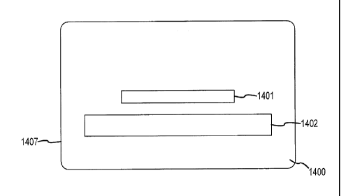
card body. For example, card body 1407 has pocket 1401 milled to accept back
panel 1406.
Also for example, card body 1407 has pocket 1410 milled to accept microchip
1403. As a
further example, card body 1407 has pocket 1402 milled to accept a signature
panel. The
procedure for creating this pocket via milling is described below with
reference to the card
making process 1308.
A back panel may be any layer of metal. A back panel may be any layer of
plastic.
The metal used to construct the back panel may be any metal or metal alloy.
For example,
titanium, stainless steel, alloys thereof and combinations thereof may be used
to construct
the back panel. A back panel may be prepared 1301, 1305 by any method
discussed herein.
A back panel may be cut 1303, 1307 from a sheet of metal. Any method of
cutting metal
disclosed herein may be used to cut a back panel from a sheet of metal. A back
panel may
have the standard transaction card dimensions. In one embodiment, the back
panel may
- 19 -
CA 02725186 2010-11-22
WO 2009/142656
PCT/US2008/079016
include one or more dimensions that are smaller than a card body (as farther
described
below).
A card body may have indicia disposed on, within or above a surface. Indicia
include legal notices, regulatory compliance messages, phone numbers, URLs,
email
addresses, trademarks, pictures, graphics, bar codes, or any other readable or
understandable
symbol. Indicia may be disposed in any manner suitable for the material of the
card body.
For example, indicia may be printed onto the card body. Printing may be
completed with
any suitable type of ink that bonds to metal or plastic. Also for example,
indicia may be
etched onto the card body. Etching may be accomplished by a laser. Etching may
be
accomplished chemically, or through milling, grinding, pressing, stamping,
embossing or
scratching. For example, indicia 1404 may be pressed or embossed onto a card
body 1407.
Also for example, indicia 1408 may be laser etched onto card body 1407. As an
additional
example, indicia 1409 may be printed onto card body 1407. To facilitate the
pressing or
embossing of indicia onto a card body, a pocket may be milled on one surface
of the card
body. Milling may involve the removal of card body material over an area.
After a pocket is created, a pressing, stamping or embossing process may be
used to
create indicia. The embossing of the characters may be applied on the surface
of the
titanium within the pocket, such as with an addressograph machine. The
pressing, stamping
or embossing may be completed within the pocket so that the embossing may be
completed
in a portion of the titanium or other metal that is thinner than the total
thickness of the
transaction card. Pressing, stamping or embossing indicia in thinner titanium
may be easier,
and may provide clearer and more visible characters on the other side of the
metal surface,
without distortion or warping of the characters or of the card body itself.
The indicia made
by pressing or embossing may be raised above the surface that is opposite the
pocket.
Pressing, stamping or embossing metal to create raised indicia may create
indicia that are
sharp or otherwise inconvenient to use in a transaction card. As such, raised
indicia may be
further milled, polished, ground, or otherwise reduced in thickness.
A back panel may have indicia disposed on a surface. Indicia include legal
notices,
regulatory compliance messages, phone numbers, URLs, email addresses,
trademarks,
pictures, graphics, bar codes, or any other readable or understandable symbol.
Indicia may
be disposed in any manner suitable for the material of the back panel. For
example, indicia
may be printed onto the back panel. Printing may be completed with any
suitable type of
ink that will bond to metal or plastic. Also for example, indicia may be
etched onto the back
- 20 -
CA 02725186 2010-11-22
WO 2009/142656
PCT/US2008/079016
panel. Etching may be accomplished by a laser. Etching may be accomplished
chemically.
or through milling, grinding, pressing, embossing or scratching. For example,
indicia 1405
may be printed on back panel 1406. In many jurisdictions, transaction cards
are required to
display particular pieces of information. A back panel having indicia disposed
thereon is
one approach to fulfilling certain requirements for different regions. By
disposing indicia on
a back panel, one card body may be manufactured and then paired with an
appropriate back
panel. This reduces production costs while still allowing a transaction card
issuer to comply
with applicable regulations.
A back panel may be bonded to a card body. Bonding 1304, 1309 may be
accomplished by coupling a back panel and a card body and subjecting the
combination to
suitable temperatures and pressures. Any pressure suitable for bonding may be
used.
Bonding may occur at any pressure high enough so that bonding would be
effective.
Bonding may occur at any pressure lower than that which would unacceptably
deform either
the card body or back panel. Any suitable temperature suitable for bonding may
be used.
For example, bonding may occur at about 275 degrees F (135 degrees C).
Further, bonding
may occur at any temperature high enough so that bonding would be effective.
Bonding
may occur at any temperature lower than that which would melt or otherwise
unacceptably
deform either the card body or back panel. Bonding may take place over any
suitable
amount of time. Bonding time may be dependent on the temperature and pressure
used. For
example, bonding may occur over the course of 15 seconds. Bonding may be
performed
with no adhesive. Bonding may be performed with an adhesive disposed between
the card
body and the back panel. Many adhesives are known in the art that are suitable
for such a
process. For example, ABLEBOND 931-1T1N1 may be used.
A card body may have a microchip disposed thereon. The position of the
microchip
on the card may be standardized by industry practice (for example, ISO 7816).
Many
jurisdictions may now require a microchip in transaction cards. The high
temperatures and
pressures that may be associated with a bonding process may damage any
microchip or
other semiconductor disposed on or in a card body. To minimize this risk, the
back panel
may be positioned on the card body such that the high temperatures and
pressures of the
binding process do not damage the microchip. Positioning the back panel below
a signature
panel may avoid damage to a microchip during the milling process. For example,
a back
panel may have a size of 3.056 in by 0.829 in. A back panel may be bonded to a
card body
such that the distance from the bottom of the card body to the bottom of the
back panel is
- 21 -
CA 02725186 2013-01-16
0.13 in. A back panel may be bonded to a card body such that the distance from
the bottom
of the card body to the bottom of the back panel is less than 0.13 in. A back
panel may be
bonded to a card body such that the distance from the top of the card body to
the top of the
back panel is 1.171 in. A back panel may be bonded to a card body such that
the distance
from the top of the card body to the top of the back panel is less than 1.171
in. A back panel
may be bonded to a card body such that the distance from each side of the card
body to each
side of the back panel is 0.159 in. A back panel may be bonded to a card body
such that the
distance from each side of the card body to each side of the back panel is
less than 0.159 in
or more than 0.159.
A microchip may be disposed onto a card body in a variety of ways. A card body
may have material removed across an area to accommodate a microchip. For
example, a
pocket may be milled into the card body. A pocket may be milled so that a
microchip may
sit flush with the surface of the card body. An adhesive may be disposed in
the pocket or on
the microchip prior to positioning a microchip into a pocket in a card body.
Any suitable
adhesive may be used. For example, ABLEBOND 931-1 T1N1 may be used for this
purpose. Further, in various embodiments, an insulating material may be
disposed in the
card body pocket to be positioned between the microchip and the card body so
as to
electrically insulate the microchip and the card body. An adhesive may act as
an insulating
material. Any insulator may be used for this purpose. Insulating properties
may be
beneficial as when the card body is made of metal, contact between the card
body and some
kinds of microchips may cause an electrical failure.
It should be noted that various changes and modifications to the presently
preferred
embodiments described herein will be apparent to those skilled in the art.
Such changes and
modifications may be made without departing from the scope of the present
invention and without diminishing its attendant advantages. It is, therefore,
intended that such changes and modifications be covered by the appended
claims.
Benefits, other advantages, and solutions to _problems have been described
herein
with regard to specific embodiments. However, the benefits, advantages,
solutions to
problems, and any elements that may cause any benefit, advantage, or solution
to occur or
become more pronounced are not to be construed as critical, required, or
essential features
or elements of the invention. The scope of the invention is accordingly to be
limited by
nothing other than the appended claims, in which reference to an element in
the singular is
not intended to mean "one and only one" unless explicitly so stated, but
rather "one or
- 22 -
CA 02725186 2013-01-16
more." Moreover, where a phrase similar to 'at least one of A, B, and C' is
used in the
claims, it is intended that the phrase be interpreted to mean that A alone may
be present in
an embodiment, B alone may be present in an embodiment, C alone may be present
in an
embodiment, or that any combination of the elements A, B and C may be present
in a single
embodiment; for example, A and B, A and C, B and C, or A and B and C. Although
the
invention has been described as a method, it is contemplated that it may be
embodied as
computer program instructions on a tangible computer-readable carrier, such as
a magnetic
or optical memory or a magnetic or optical disk. All structural, chemical, and
functional
equivalents to the elements of the above-described exemplary embodiments that
are known
to those of ordinary skill in the art are intended to be encompassed by the
present claims. Moreover, it is not necessary for a device or method to
address each and every problem sought to be to solved by the present
invention, for it to be encompassed by the present claims. Furthermore, no
element,
component, or method step in the present disclosure is intended to be
dedicated to the public
regardless of whether the element, component, or method step is explicitly
recited in the
claims. As used herein, the terms "comprises", "comprising", or any other
variation thereof, are intended to cover a non-exclusive inclusion, such that
a
process, method, article, or apparatus that comprises a list of elements does
not include only those elements but may include other elements not expressly
listed or inherent to such process, method, article, or apparatus.
- 23 -