Note: Descriptions are shown in the official language in which they were submitted.
CA 02725309 2010-12-14
Case 3019
METHOD OF MANUFACTURING ELECTRONIC CARDS
Field of the invention
The present invention concerns a method of manufacturing complex
electronic cards each including a first electronic unit, at least partially
arranged in a window in a solid layer of the card, and a second electronic
unit electrically connected to the first electronic unit and incorporated in
an
internal layer formed by a filler material which covers at least one of the
surfaces of said second electronic unit. In particular, the filler material is
a
resin, provided in a non solid state during the manufacturing process or a
resin provided in the form of at least partially melted hot melt sheets, so as
form an internal layer of the card. It will be noted that the internal layer
formed by the filler material can contain other solid structures or elements,
in particular positioning or filler structures for said internal layer.
"Electronic card" means a bank type card and also other devices in
various forms, particularly an electronic tag or a portable electronic device.
Background of the invention
A method is already known from EP Patent No. 1,559,068 for
manufacturing electronic modules which each include two insulating sheets
defining the external faces thereof, at least one electronic element having
an external surface that substantially touches one of the external surfaces
of the electronic module and an electronic circuit arranged between the two
insulating sheets and connected to the electronic element. This method
provides the following steps:
- providing at least a first insulating sheet including a window for
housing the electronic element;
CA 02725309 2010-12-14
-2-
- inserting the electronic instrument in the window of the first
insulating sheet, said electronic element being provided with conductive
connection pads arranged on an inner surface opposite to the external
surface thereof;
- superposing an adhesive protective film that extends at least into
the area between the electronic element and the edges of the window, the
protective film holding the electronic element in the window and closing any
slit between said electronic element and the lateral wall of said window;
- placing the electronic circuit in a zone close to the window and
connecting the electronic element to the electronic circuit through a window
provided or made in the protective film and located opposite said
conductive connection paths;
- depositing a filler material on the set of elements already provided
and superposing a second insulating sheet on the filler material;
- pressing or laminating the assembly produced by the preceding
steps, the filler material forming a layer compensating for any surface
contours resulting from assembling the electronic module.
The manufacturing method described above solves an important
problem, namely, preventing the filler material, generally formed by a resin
which is in a viscous liquid state when pressure is applied to form the
electronic module, from flowing into any slit between the electronic element
and the lateral wall of the window in which it is arranged, so as to prevent
the resin extending at least partially onto the visible external surface of
the
electronic element. However, the manufacturing method presents a
problem in relation to the sequence of steps, in particular the fact that the
electrical connection between the visible electronic element and the internal
electronic unit is achieved once the electronic element has been inserted in
a window in an external insulating layer of the card being manufactured and
the adhesive protective layer is in place. This sequence of steps raises a
practical problem given that card manufacturing equipments or facilities are
not generally equipped with a device for welding or assembling various
CA 02725309 2010-12-14
-3-
electronic units. Indeed, generally, the various electronic circuits and
elements are first assembled to form electronic devices and then these
electronic devices are taken to a conventional card manufacturing
equipment or facility in which the various materials used to form the cards
are provided and processed in an appropriate manner to obtain high quality
electronic cards into which the electronic devices are respectively
incorporated. The aforecited Patent of the prior art does not propose
temporally separating production of the electronic devices from the
manufacture of the cards incorporating these electronic devices. Although
the method described in the aforecited document can be implemented and
used to obtain complex electronic cards, it has a major drawback for those
skilled in the art specialised in manufacturing finished electronic cards or
inlets, who prefer to separate the production of the electronic devices from
the card forming process.
It is an object of the present invention to overcome the major
drawback of the prior art method mentioned above.
Summary of the invention
The electronic card manufacturing method according to the invention
is mainly characterized in that the electronic assembly or device, formed by
at least a first electronic unit provided in a window in a solid layer of the
card and by a second electronic unit arranged in an inner layer or the body
of said card, is manufactured first, prior to production of the electronic
cards; i.e. before the solid layers and other materials forming the body of
the card are added. Thus, the electronic device incorporated into each card
is made in a preliminary step, in accordance with a conventional process. In
order to do this, various ways of implementing the card manufacturing
method are proposed. In particular, according to the invention the protective
film is formed of several parts or a single part with at least one slit.
CA 02725309 2010-12-14
-4-
If the protective film is in several parts, these parts have
complementary profiles that can cover the external edge of a rear face of
the first electronic unit, while extending into the entire peripheral zone of
said first electronic unit and defining a window allowing the electrical
connection between the first and second electronic units to pass through.
This window thus has smaller dimensions than those of the first electronic
unit. Thus, once the electronic device has been taken to the card
manufacturing equipment or facility and the first electronic unit has been at
least partially inserted into a window in the first solid layer, the
protective
film can properly cover any slit between the lateral wall of the window and
the first electronic unit.
If the protective film is formed of a single part with at least one slit,
this slit is either a through slit between a central window in the film and
the
outer edge thereof, said slit thus being able to be moved aside to allow the
electrical connection to pass inside said central window, or, when the slit is
not a through slit, it is arranged such that the first or second electronic
unit
can pass through the central window in the protective film by moving aside
the parts of said protective film located at the edge of said window.
The electronic card manufacturing method according to the invention
includes three main implementation modes. In a first implementation mode
of the invention, as described in claim 1 annexed to this description of the
invention, the electronic device, formed of at least first and second pre-
assembled electronic units, is first of all brought to the card manufacturing
equipment or facility where the first electronic unit is placed in a window in
a
first solid layer. Next, a protective film of the type described above is
provided and arranged so as to cover essentially any slits that may exist
between the first electronic unit and the lateral wall of the window.
According to the second implementation mode defined in claim 2
annexed to this description of the invention, the electronic assembly or
device is first of all made and then, before the electronic device is provided
on a first solid layer and the first electronic unit is arranged in the window
in
CA 02725309 2010-12-14
-5-
said solid layer, the protective film is assembled to said electronic device
so
that the electrical connection is located in a window defined by the
protective film and so that the latter is thus located between the first and
second electronic units. Next, the pre-assembled electronic device and
protective film are taken to the card manufacturing equipment or facility
where said solid layer is provided, the first electronic unit is conveniently
inserted in the aperture provided in the solid layer, and the protective film
is
applied across a zone peripheral to the window and, if this has not been
previously done, at least against the lateral surface and/or the outer edge of
a rear face of the first unit. In a variant of this second embodiment, a
protective film is first of all assembled to said first unit by applying said
film
at least against the outer edge of a rear face of said first unit, then an
electrical connection is established with the second electronic unit through
an aperture in said film before the protective film pre-assembled with the
electronic device is taken to a card manufacturing equipment or facility
where the first solid layer is added.
According to the third implementation mode of the invention, as
defined in claim 6 annexed to this description of the invention, firstly the
electronic assembly or device is manufactured, formed of at least the first
and second electrically connected electronic units, and then a structure
including a protective film having at least one window, which has smaller
dimensions than those of the first electronic unit and has flaps at the
periphery thereof, separated by slits, and a first solid layer having at least
one window for at least partially receiving the first electronic unit. Said
protective film is assembled to the first solid layer with said at least one
aperture centred on said at least one window. Next, said structure and said
electronic device are taken to a equipment or facility and the first
electronic
unit is placed opposite said aperture, then said first unit is pushed into
said
window by folding said flaps towards the lateral wall of the aperture until
the
flaps are released and then moved back up at least partially in the direction
of the general plane of the protective film. Next, the first unit is moved
back
CA 02725309 2010-12-14
-6-
up in the direction of said aperture and said flaps are at least partially
applied against the lateral surface and/or a rear face of said first unit, so
as
to close any slits between the lateral wall of the window and the first unit,
said electrical connection passing through said aperture.
Finally, in the method according to the invention a filler material is
provided on the protective film, in particular a resin, which is at least
partially in a non solid state when a layer or body of the cards is at least
partially formed by the filler material, the latter at least partially
covering said
electrical connection of said electronic assembly or device.
It will be noted that, in a variant, the protective film has an adhesive
surface that holds it in place and also, in a subsequent step of depositing a
filler material at least partially covering the electronic connection,
prevents
said filler material from infiltrating underneath the protective film and thus
flowing into the window. Other variants for holding the protective film in
place can be envisaged. For example, the solid layer may have an adhesive
top surface in the area provided for the protective film. In another variant,
the protective film is thermally welded to the solid layer, particularly in
several specific areas.
Various variants of the manufacturing method according to the
invention form the subject of the dependent claims.
Brief description of the drawings
Other features and advantages of the electronic card manufacturing
method according to the invention will also appear from the following
detailed description of implementation modes of this method, this
description being made with reference to the annexed drawings, given by
way of non-limiting example and in which:
CA 02725309 2010-12-14
-7-
- Figure 1 shows a first embodiment of the electronic device
incorporated in each card manufactured in accordance with the method of
the invention;
- Figure 2 shows the electronic assembly or device of Figure 1
assembled with a protective film;
- Figure 3 is a top view of an electronic card according to the
invention in an intermediate state during the manufacturing method of the
invention;
- Figure 4 is a cross-section along the line IV-IV of Figure 3 with the
electronic card in a finished or semi-finished state;
- Figure 5 is a cross-sectional view along the line V-V of Figure 3 with
the electronic card in a finished or semi-finished state;
- Figures 6A and 6B illustrate respectively two variants of a protective
film according to the invention;
- Figure 7 shows schematically a second embodiment of an
electronic device incorporated into each card manufactured in accordance
with the method of the invention;
- Figure 8 is a cross-sectional view of a card obtained via the method
according to the invention and incorporating the electronic device of Figure
7;
- Figure 9A shows schematically one step of a second
implementation mode of the method according to the invention;
- Figure 9B partially shows the intermediate product resulting from
the step shown in the diagram of Figure 9A;
- Figure 10 shows a cross-section of a variant of an electronic card
obtained via the method according to the invention;
- Figure 11 is a top view of a protective film for producing a batch of
cards in accordance with a third implementation mode of the method of the
invention; and
- Figures 12A, 12B, 12C, 12D and 12E show a series of steps
occurring in the aforementioned third implementation mode.
CA 02725309 2010-12-14
-8-
Detailed description of the invention
With reference to Figures 1 to 5, a first implementation mode of an
electronic card manufacturing method according to the invention will be
described below.
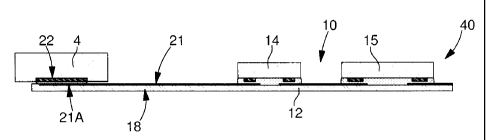
In a preliminary step of this card manufacturing method, a first
electronic unit 4 is assembled to a second electronic unit 10 to form
electronic assembly or device 40. Electronic unit 10 is formed of a PCB type
support 12 at the surface of which various components 14, 15 and 16 are
arranged. These electronic circuits can be formed of any type of component
and may have various functions. Component 14 can for example be a
micro-processor, component 15 a display and component 16 a battery. It
will be noted that the second electronic unit 10 can also, in a variant, form
a
battery or, in another variant, form an antenna. It will also be noted that
the
first electronic unit can be formed by a single external electric contact pad
connected to an internal electronic unit of the card.
PCB 12 can be rigid or flexible. This support 12 is extended by a
tongue 18 which is flexible, or at least capable of undergoing elastic
deformation. Conductive paths 20 and 21 for establishing electrical
connections between unit 10 and unit 4 are arranged on tongue 18. For this
purpose, unit 4 has electrical connection pads 22 to which end pads 20a
and 21A of paths 20 and 21 are electrically connected, particularly by tin
welding or using a conductive adhesive. The tin can be deposited
beforehand in the form of a thin film at the surface of contact pads 22. It
will
be noted that, according to the terminology used for this description of the
invention, tongue 18 fitted with conductive paths forms an electrical
connection between the first electronic unit 4 and the second electronic unit
10. It will be noted that the electrical connectiondescribed here is an
advantageous example, but that any type of electrical connection between
two electronic units known to those skilled in the art can be envisaged. In
CA 02725309 2010-12-14
-9-
particular, more than two conductive paths or electrical connections can be
provided between the two units. Tongue 18 can act as a support for a large
number of electric connection paths between the two electronic units.
After electronic device 40 has been formed, a protective film in two
parts 24 and 26 is provided, the respective profiles of said parts defining,
when assembled, a central aperture 32 into which electrical connection 18
passes, said aperture having smaller dimensions than those of first
electronic unit 4. The two part protective film is arranged between the first
and second electronic units 4 and 10, with electrical connection 18 passing
through aperture 32. In the variant shown, the two parts have a general U
shape. In another variant, only one of the two parts is U-shaped or both
parts are L-shaped. The protective film has a zone peripheral to aperture 32
which is applied against the outer edge 5 of the rear face of first electronic
unit 4. Protective film 24, 26 then extends into a zone peripheral to first
unit 4 as shown in Figure 2. The function of the protective film will be
described below.
Electronic devices 40 fitted with the protective film are then taken to
an electronic card production equipment or facility where several cards or
inlets are generally manufactured simultaneously in the form of a plate or
sheet. In the equipment or facility, a first solid layer is provided, said
layer
having at least one window 6 provided for each card and intended to
receive at least partially the first unit 4 of electronic device 40. Each unit
4 is
thus placed in a window 6 in solid layer 8. The protective film is then
applied
against the peripheral zone of window 6 so as to close any slit 28 between
the lateral wall 30 of said window and first unit 4. To ensure that slit 28 is
entirely closed by the protective film, the two parts 24 and 26 thereof have a
zone 34 where the parts are superposed, part 26 having a region that
partially covers part 24. In a variant, it is, however, possible to omit the
overlapping zone, but to assembly the two parts properly side by side
without leaving any space between them.
CA 02725309 2010-12-14
-10-
In a subsequent step, a filler material 42 is provided on first solid
layer 8 and on the protective film, and pressure is for example applied to
the filler material which is then in a non solid state, to form a layer of the
electronic cards being manufactured, with the filler material surrounding
electrical connection 18.
In the variant shown in Figures 4 and 5, before pressure is applied to
filler material 42, a second solid layer 44 is provided on said filler
material.
Preferably, the protective film includes an adhesive or heat-reactivatable
surface allowing said protective film to be fixed firstly to the rear face of
unit 4 and/or said protective film to be bonded to the top surface of solid
layer 8. The fact that the protective film is in two or more parts means that
it
can easily be arranged at the edge of the rear face of electronic unit 4 while
defining an aperture 32 that allows electrical connection 18 to pass through.
Owing to this feature, it is thus possible to arrange the protective film
properly after electronic device 40 has been formed.
It will be noted that the electronic device can include more than two
units, in particular at least two units at least partially arranged in
respective
windows in one or two solid layer(s) so as to be visible.
Figures 6A and 6B show two variants of another embodiment of the
protective film which also satisfies the objective of the present invention.
Protective film 50 of Figure 6A is formed of a single part defining a central
aperture 32 and having a slit 52 which passes through film 50 from
aperture 32 as far as the external edge of said film. It is thus of the slit
ring
type. Again, so as to be able to arrange an area of film 50 peripheral to
aperture 32 against the outer edge of the rear face of unit 4, aperture 32
has smaller dimensions than those of unit 4. The electrical connection 18
can easily be arranged in aperture 32 by inserting connection 18 into slit 52,
and then moving it until it is located in aperture 32. Next, film 50 is
correctly
placed against the rear face of unit 4 in a similar way to the arrangement
shown in Figures 2 and 4.
CA 02725309 2010-12-14
-11-
Protective film 54 of the variant shown in Figure 6B differs in that a
plurality of slits 56a to 56d is arranged at the periphery of aperture 32.
These slits do not pass through film 54 as far as the outer edge thereof.
They can therefore define parts peripheral to aperture 32, which can easily
be folded outside the general plane of film 54 and thus allow an electronic
unit, of larger dimensions than those of aperture 32, to pass through. To
arrange protective film 54 between the first and second units 4 and 10 of an
electronic device 40 in accordance with the present invention, unit 4 is
pushed through aperture 32 moving aside the parts peripheral to said
aperture 32 located between slits 56a to 56d. These peripheral parts thus
undergo elastic deformation and return into the general plane of protective
film 54 once unit 4 has passed through. The electrical connection 18 is then
in aperture 32. So as to limit as far as possible any flow of resin into any
slit
or generally of any filler material deposited when the card body is being
formed, the slits preferably have a minimum or zero width. "Slit" therefore
means in particular making a simple cut in the protective film, particularly
along a straight line portion.
The filler material provided to form the core of the card or an internal
layer of said card is preferably formed by a resin deposited in viscous liquid
state or in the form of a hot melt solid which is then at least partially
melted
so as to coat second electronic unit 10. According to a preferred
implementation of the step of forming the core or internal layer of the card,
firstly the second units 10 are rotated by elastically folding electrical
connection 18, units 10 then being turned onto their top side on the other
side of aperture 6 relative to the side provided for these units in the centre
of the finished card. In a variant, units 10 are simply raised by suitable
means and placed for example momentarily in a substantially vertical
position. Next, a first part of the filler material is placed on bottom solid
sheet 8, so that this first resin part at least partly covers the areas of
said
layer 8 where units 10 will eventually be arranged. Then, electronic units 10
are folded down or rotated again onto the bottom side thereof and placed
CA 02725309 2010-12-14
-12-
on the first part of the filler material deposited beforehand. A second part
of
the filler material is then placed on units 10 so that the filler material
completely coats the units and most of electrical connection 18. This
method ensures that the filler material is present underneath
components 14 to 16 of unit 10. This thus avoids some parts of bottom
layer 8 not being coated with resin; which could then cause subsequent
surface deformation problems for the finished card.
According to an alternative implementation of the method of the
invention, in particular in the situation described with reference to Figures
1
to 5, the resin is essentially provided during a single same step and then
spread out by using a roller or blade in one direction which ensures that part
of the resin thereby spread out penetrates beneath support 12 of unit 10.
This is made easier because the electronic components of unit 10 are
located underneath said support. Thus, support 12 is initially located at
some distance from solid layer 8 and a resin in a viscous liquid state easily
penetrates beneath and also partly above said support during the step of
forming a resin layer. It will be noted here that, in a variant where the
electronic device 40 is manufactured so that the components of the second
unit 10 are located above support 12 once the first unit 4 has been
arranged in the aperture of the bottom layer, means can be provided to
assist the flow of part of the resin underneath support 12. By way of non-
limiting example, this support can have small projecting portions thus
creating an empty space between said support and the bottom solid layer.
Apertures can also be provided in support 12 to encourage the flow of part
of the resin underneath said support. In a variant, support 12 can have a
raised end part, particularly defining an inclined plane. The resin is then
spread out by a roller or a blade in a direction that tends to lift the second
internal electronic units, the horizontally pushed resin pressing against
these raised parts relative to the general plane of support 12 and thus
exerting an upward thrust. In a variant, the resin is introduced laterally
between the two solid layers 8 and 44, particularly by injection into a mould.
CA 02725309 2010-12-14
-13-
According to another alternative implementation of the method
according to the invention, in the aforementioned case where support 12 of
the second electronic unit 10A is provided underneath the electronic
components of the second unit, a resin film 60 is deposited beforehand
underneath support 12. This resin film may be similar in nature to a resin
film 62 deposited underneath protective film 50 (Figure 7).
According to the embodiment of the electronic device 40A of
Figure 7, the electrical connection 64 between units 4a and 10A is formed
by metal tongues which come out of module 14A. These metal tongues can
be deformed and allow protective film 50 to be easily arranged against the
rear face of unit 4A. It will be noted that unit 4A has a lateral wall with a
recess. As shown in Figure 8, electronic device 40A is then arranged on a
solid layer 8A having apertures 6A with steps against which the top part of
unit 4A rests. Solid layer 8A can be formed of two layers laminated to each
other and each having an aperture of different dimensions to define a
housing having a cross-sectional profile matching that of unit 4A. In the
embodiment of a card according to the invention shown in Figure 8, two
transparent external films 66 and 68 are finally added. It will be noted that
transparent film 66 covers electronic unit 4A. The latter forms, for example,
a light sensor, a solar sensor, or a light emission source, in particular
within
the infra-red range. Unit 4A can also define an electronic display visible
through transparent film 66.
It will also be noted that resin film 60 located between layer 8A and
support 12 can be identical to resin 42 forming the internal layer of the
card.
Adhesive film 60 can be made to adhere to the bottom layer by applying
heat through said layer.
With reference to Figures 9A, 9B and 10 a second implementation
mode of the card manufacturing method according to the present invention
will now be described. This essential difference between this second
implementation mode and the first mode is a variation in the sequence of
steps of the method. As shown schematically in Figure 9A, electronic
CA 02725309 2010-12-14
-14-
assembly or device 40B is firstly provided on bottom solid layer 8 and
unit 4B is inserted into cavity 6 provided in said layer. It will be noted
here
that one part 42A of the resin, intended to form an internal layer in which
electronic unit 10B is incorporated, is provided before device 40B or, in a
variant, this resin part 42A is added while unit 10B is raised or turned over,
as was described previously. Once the first unit 4B is partially housed inside
aperture 6 of solid layer 8, protective film 50 is provided and set in place
as
shown in Figure 9B, by inserting the electrical connection 64A in
aperture 32 of film 50, through slit 52 provided in said film (Figure 6A). It
will
be noted that unit 4B can be secured to the layer by dots of adhesive before
the protective film is arranged. This film is formed in this variant of a
single
part having at least one slit starting from an aperture made in said part, the
dimensions of said aperture being smaller than those of first unit 4B.
Protective film 50 is set in place so that it covers a peripheral zone of
window 6 and the outer edge of the rear face of first unit 4B where electrical
connection pads 22 are arranged. This arrangement according to the
invention allows any slit between the lateral wall of each window provided in
solid layer 8 and the first unit 4B placed in said window to be closed. As in
the first implementation, the protective film can be formed of several parts
with respective profiles which, when assembled on the bottom solid layer 8,
define an aperture into which the electrical connection 64A passes.
Then, as in the first implementation mode of the invention, a filler
material, particularly a resin, is deposited on the first solid layer 8 and
protective film 50, and the filler material is spread out in a non solid state
to
form a layer of the electronic cards, said filler material then covering the
second electronic unit 10B.
The card variant shown in Figure 10 differs in particular from that of
Figure 8 in that the bottom transparent film 70 has a window 72 arranged
opposite the external surface of the first unit 4B. Electronic unit 4B here
forms for example a fingerprint sensor. This latter variant has the advantage
CA 02725309 2010-12-14
-15-
of closing any slit between unit 4B and the lateral wall of window 6 on the
side of the external surface of solid layer 8.
It will be noted that, in the various card embodiments described
above, the dimensions of the protective film are limited such that it does not
extend underneath the whole of the second electronic unit incorporated in
the resin layer. In particular, the protective film has reduced dimensions and
is not superposed on the second internal unit incorporated in the resin
layer. This thus avoids having a film covering most of the bottom solid layer
and thus forming an interface between the resin layer and the bottom solid
layer. Even if the protective film has adhesive or heat-reactivatable
surfaces, the adherence of the film to the bottom solid layer may be
reduced. A protective film passing through the card could thus cause
peeling problems for the bottom solid layer.
With reference to Figures 11 and 12A to 12E, a third implementation
mode of the electronic card manufacturing method according to the present
invention will be described below. This implementation is particularly suited
to automated production and provides cards of very high quality, without
any risk of the protective film peeling off.
Protective film 76 is made for several batch manufactured cards, in
the form of a plate from which the cards are then cut out. This film 76 has
apertures 32A for the electrical connections 64, of electronic assemblies or
devices 40C incorporated in the cards, to pass through, and preferably
apertures 78 in the zones provided for the second electronic units 10C.
Each aperture 32A has four flaps 80a to 80d defined by four slits 82
provided in the corners of said aperture 32A. It will be noted that the
protective film is very thin here.
In a first step of the card production method, film 76 is assembled by
lamination, preferably hot lamination, with a solid layer 8 having apertures 6
for receiving respectively the first units 4 of the prefabricated electronic
assemblies or devices 40C. This solid layer and the protective film thus
CA 02725309 2010-12-14
-16-
adhere securely to each other. Apertures 32A are centred on apertures 6.
Flaps 80a - 80d are then located along the perimeter of each aperture 6 in
the general plane of protective film 76. It will be noted that the slits can
be
made after the lamination step, particular in the case of hot lamination.
Next, the electronic devices 40C are placed on the structure formed
of bottom layer 8 and protective film 76 (Figure 12A) and the first units 4
are
pushed into apertures 6 by folding flaps 80a - 80d against the lateral wall 30
of said apertures (Figure 12B). Units 4 are lowered sufficiently to release
said flaps which then move at least partially back up towards the general
plane of film 76 (Figure 12C). Finally, units 4 are moved up inside apertures
6 to the level anticipated for the finished cards (Figure 12D). The flaps are
then abutting against the lateral surface of unit 4. To close the slit
securely
between unit 4 and wall 30 of aperture 6 in which it is inserted, the ends of
the flaps are preferably folded against the outer edge of the rear face of
unit 4 (Figure 12E). These folded ends are preferably bonded against said
rear face. Again slits 82 may have almost zero width. Thus when the resin
is subsequently deposited on film 76, electronic units 10C and their
respective electrical connections 64 to units 4, the resin will not flow along
walls 30 of windows 6. The subsequent steps are similar to those of the
other implementations modes of the method, as are the variants that can be
envisaged for these subsequent steps. They will not be described again in
detail here.
In a variant that is not shown, the first electronic unit has a narrowed
portion in the internal part thereof, this narrowed portion defining, on the
top
internal surface of solid layer 8, a horizontal peripheral surface of said
first
unit substantially in the plane of said top internal surface while the height
of
the first first unit can be considerably greater than the thickness of the
solid
layer. When the first unit is moved up into its final position, the flaps of
the
protective film are then located on said peripheral surface of said first unit
in
a horizontal position. The slits in the corners of the aperture can thus be
properly closed since the flaps are located in the general plane of the
CA 02725309 2010-12-14
-17-
protective film; which guarantees a high level of sealing when the filler
material passes in its non solid state, in particular a resin in a viscous
liquid
state.
It will be noted that, in the variant shown in Figure 12A, the bottom
surface of internal unit 10C has bumps or raised portions which leave a
space free between the internal unit and the top surface of layer 8 so as to
allow the resin to fill this space when an internal layer of the cards is
being
formed and thus form a resin film that securely fixes unit 1 OC to layer 8.