Note: Descriptions are shown in the official language in which they were submitted.
CA 02725723 2010-11-23
WO 2009/151941 PCT/US2009/045129
1
MULTI-LAMPS INSTANT START ELECTRONIC BALLAST
FIELD OF THE INVENTION
[0001] The present invention relates to electronic ballasts, and more
specifically, to
series resonant ballast inverters for operating multiple discharge lamps. In
addition, it relates to
ballast starting and steady-state operation of a variable number of lamps (for
instance, from 0
lamps to 4 lamps) to maintain a constant brightness level of the lamps.
BACKGROUND OF THE INVENTION
[0002] Gas discharge lamps utilize electronic ballasts for converting an AC
line
voltage into a high frequency current for powering the gas discharge lamps.
Instant start ballasts
typically supply power to several lamps in a fixture. The instant start
ballast is frequently used
for lamp starting without preheating the lamp filaments. For example, the
industry standard,
instant start electronic ballast for multiple T8 lamps employs a current fed
parallel resonance
inverter. Since this inverter is a voltage source rather than a current
source, each of these lamps
is connected to the inverter output via a boost capacitor. A difference
between a current fed half
bridge resonance inverter and a voltage fed series resonance half bridge
inverter is that in the
current fed inverter maximum voltage across switching transistors is more than
twice as high as
the voltage fed inverter. A half bridge current fed ballast inverter requires
high voltage
transistors (1100V and higher), whereas in a half bridge voltage fed series
resonant inverter the
maximum transistor voltage is much lower, i.e., it is equal to the DC bus
voltage (430-440V).
Voltage fed resonant inverters tend to be more efficient than current fed
resonant inverters
because voltage fed inverters utilize MOSFETS in a Zero Voltage Switching
(ZVS) mode. In
addition, the lamp current generated by voltage fed series resonant inverters
is almost sinusoidal.
It provides longer lamp life than a current fed inverter. Also, voltage fed
series resonance
inverters can be built without an output power transformer.
CA 02725723 2010-11-23
WO 2009/151941 PCT/US2009/045129
2
[0003] To take advantage of voltage fed inverters, multi-lamp ballasts
sometimes are
provided with several identical resonant tanks, each coupled to a single
discharge lamp. For
example, US Patent 7,372,215 issued to Sekine et al. discloses a multi-
parallel lamp ballast with
a single inverter and multiple resonant tanks. In addition to complexity, the
above ballast needs
to be restarted after replacing a lamp. It is provided with lamp out/in
sensing to activate the
restart. Patent Application 2007/0176564 issued to Nerone at al. discloses a
multi-lamp
application of a voltage fed self generated inverter having a regulated output
voltage. This
inverter is provided with output voltage clamping means since its control does
not have enough
resolution to limit this voltage at no load. Also, it has a number of multi-
winding magnetic
components which affect ballast cost.
[0004] One challenge in designing a multi-lamp series resonant ballast is to
control
both the wide range of load variations and the need for sufficient start up
voltage. A few of such
series resonant ballasts for powering multi-parallel lamps are known. For
example, US Patent
6,362,575 issued to Chang et al. discloses a control circuit for a four lamp
transformerless series
resonance inverter with regulated output voltage. Four boost capacitors, each
connected in series
with a lamp, are used for ballasting gas discharge lamps. The ballast senses
the number of lamps
connected by monitoring the current via lamp filaments and generates reference
voltages
according to number of lamps connected to the ballast. The above approach
requires additional
wiring between the ballast and the lamps. US Patent 7,352,139 issued to
Ribarich et al. discloses
a static feedback control circuit for a multi-lamp series resonant inverter
with a control IC
utilizing a voltage control oscillator (VCO) for frequency control. Since VCO
oscillations are not
phase locked with resonant load oscillations, the VCO cannot follow changes in
resonant load
fast enough and may not always oscillate above the resonant frequency.
According to the above
patent application, the VCO integrates its input signal, causing a delay in
dynamic frequency
response. During transients in the resonant load (a gas discharge lamp may
significantly change
CA 02725723 2010-11-23
WO 2009/151941 PCT/US2009/045129
3
its resistance in few microseconds) or lamp removal, this delay can cause
temporarily hard
switching in the inverter MOSFETS and damage the inverter. ICs with adaptive
ZVS (IR 2520D
and other similar adaptive circuits) do not eliminate the cross conduction
phenomena in
switching transistors during unexpected transients in inverter load. US Patent
7,030,570 assigned
to Osram Sylvania discloses a series resonant inverter single lamp operation
in which hard
switching is avoided during load transients.
[0005] Nevertheless, there is a need for a ballast control circuit and method
aimed at
multi-lamp instant start applications. Parallel connected lamps are preferable
in multi-lamp series
resonant ballast since the light in not interrupted when replacing lamps in a
fixture. Existing
control methods for multi-lamp inverters (0 load) are based on the concept
that the resonant
inverter voltage is regulated and ballasting of lamps is achieved with series
capacitors. In one
embodiment, the present invention provides a method and control circuit for
parallel multi-lamp
instant start operations that utilize the ballasting features of both resonant
inverters and series
capacitors.
SUMMARY OF THE INVENTION
[0006] In one embodiment, the present invention provides a series resonant
ballast
inverter for plurality of gas discharge lamps (up to 4 lamps typically)
coupled in parallel. In
another aspect, an embodiment of the invention provides a series resonant
inverter for a variable
number of lamps (typically from 1 lamp to 4 lamps) wherein lamp brightness is
maintained
almost independent of the number of lamps connected.
[0007] It is the other aspect of an embodiment of the present invention to
provide a
multi-parallel lamp series resonant inverter with dimming capability.
[0008] It is the other aspect of an embodiment of the present invention to
provide a
ballast control circuit having continuous no load operation with reduced power
losses.
CA 02725723 2010-11-23
WO 2009/151941 PCT/US2009/045129
4
[0009] It is the other aspect of an embodiment of the present invention to
provide
multi-lamp ballast with ZVS inverter operation during transients.
[0010] It is the other aspect of an embodiment of the present invention to
utilize a
control IC (self oscillating half bridge driver) with minimum surrounding
components.
[0011] It is the other aspect of an embodiment of the present invention to
provide
transformerless ballast for instant start lamps with limited leakage current
satisfying electrical
shock safety requirements.
[0012] It is a still another aspect of an embodiment of the invention to
provide
electronic ballast with minimum components, a simple schematic and a low cost.
[0013] In one embodiment, an electronic ballast comprises a series half bridge
resonant inverter, a control circuit controlling the inverter switches, a
first feedback circuit
coupled between the inverter output and a control input and a second feedback
circuit coupled
between the inverter output and the control input.
[0014] In one embodiment, the electronic ballast comprises a series half
bridge
resonant inverter and a control circuit for the inverter with dimming
capability. The inverter
powers a number of gas discharge lamps connected in parallel via individual
boost capacitors.
The inverter includes a first and a second additional voltage feedback
circuits via first and
second charge pumps correspondingly coupled between the inverter output and
the dimming
input of the control circuit. The first charge pump generates a referenced
control signal to
achieve nominal lamp current/power after starting. The second charge pump
generates an error
control signal when the inverter output voltage exceeds a predetermined value.
Both signals are
summed at the dimming input of the inverter control circuit. The error control
signal prevails
during lamp starting, open circuit and reduced number of lamp operation modes.
This error
signal shifts the switching frequency higher to avoid voltage and current
stresses in the inverter
components. The referenced control signal prevails at full inverter load,
shifting operation to a
CA 02725723 2010-11-23
WO 2009/151941 PCT/US2009/045129
lower frequency and stabilizing the steady-state mode of the inverter. As a
result, the inverter
frequency changes as a function of number of lamps connected, and the inverter
operates safely
above the resonance frequency so that lamps are not overdriven.
BRIEF DESCRIPTION OF THE DRAWINGS
[0015] The invention is better understood with reference to the accompanying
drawings in which:
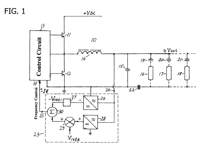
[0016] FIG. 1 is a circuit diagram of an instant start multi-lamp ballast
inverter
control circuit according to one embodiment of the invention;
[0017] FIG. IA illustrates a typical dimming characteristic (output power P
versus
DC control bias signal Ib) for the ballast inverter control circuit of FIG. 1;
[0018] FIG. 2 is a circuit diagram of an instant start multi-lamp ballast
inverter
control circuit according to another embodiment of the invention;
[0019] FIG. 3 is a circuit diagram of one embodiment of the invention;
[0020] FIG. 4 is (a prior art diagram) illustrating a family of conventional
resonant
plots of inverter output voltage Vout versus switching frequency when driving
different numbers
of lamps;
[0021] FIG. 5 illustrates an inverter transistor current and output inverter
voltage
during starting with four lamps according to one embodiment of the invention.
DETAILED DESCRIPTION OF THE INVENTION
[0022] The present invention relates to a ballast control circuit with a self
oscillating
half bridge driver IC. Unlike other control circuits for half bridge resonant
inverters having
control ICs with a VCO, it utilizes direct feed-forward control from a
resonant load that includes
lamp resistance. A time duration of any half wave formed by the inverter
depends on the lamp
resistances during formation of the half wave. The inverter control circuit is
described in Osram
CA 02725723 2010-11-23
WO 2009/151941 PCT/US2009/045129
6
Sylvania US Patent 7,095,183 "Control System for Resonant Inverter with Self-
Oscillating
Driver". Accordingly, the inverter control system is provided with a source of
regulated negative
DC bias and a voltage feedback circuit as a source of positive DC bias. Both
positive and
negative DC bias currents are summed at the frequency control input of the
resonant inverter.
The negative DC bias current is applied to the frequency control input with a
time delay relative
to a beginning point of resonance inverter starting. The voltage feedback
circuit converts the
inverter output AC voltage to a DC voltage signal and compares this voltage
signal to a reference
signal. An error signal initiates the positive DC bias. A regulated negative
DC bias current sets
the nominal current and power of the lamps coupled to the inverter after
starting. The positive
DC bias current appears when the output voltage of resonant voltage reaches a
given maximum
level, which occurs during lamp starting or when one or more lamps are
disconnected during
ballast operation.
[0023] In one embodiment of the invention, two charge pump circuits are
coupled to
the inverter output. The first charge pump converts the AC inverter output
voltage to a
referenced negative DC bias signal. The second charge pump is used in a
voltage feedback
circuit for sensing an output AC voltage and converting sensed AC signal to a
positive DC signal
voltage. This positive DC signal voltage is compared with the referenced DC
voltage and, if it
exceeds this referenced voltage, an error signal is generated. The error
signal is applied as a
positive DC bias to the frequency control input for limiting inverter output
voltage. The error
signal may be amplified for more precise voltage limiting. A voltage feedback
circuit limits the
inverter output voltage in a no load mode as well as during lamp starting and
during operation
with a reduced number of lamps. Since the charge pumps are used in this
feedback, all voltage
control functions are provided relative to the inverter RMS output voltage.
[0024] FIG. 1 shows a block-circuit diagram for a multi-parallel lamps series
resonant inverter 10 according to one embodiment of the invention.
Practically, up to four gas
CA 02725723 2010-11-23
WO 2009/151941 PCT/US2009/045129
7
discharge lamps can be connected in parallel to the output of the resonant
inverter via individual
boost capacitors. The ballast is provided with Power Factor Corrector (PFC)
converting AC line
voltage to regulated DC bus voltage VDC (PFC is not shown in FIG. 1).The input
of a half bridge
series resonant inverter 10 is coupled to regulated DC voltage bus (+VDC). The
resonant inverter
converts the DC bus voltage to a high frequency AC voltage Vout. The power
stages of
inverter 10 include switching transistors 11 and 12 driven by a control
circuit 13. The control
circuit 13 incorporates high side and low side half bridge MOSFET drivers, an
internal oscillator
(not shown in FIG. 1), and a frequency control (not shown in FIG. 1). In
general, any ballast
inverter control circuit having frequency dimming capability may be used. For
example, the
circuit described in Osram Sylvania US Patent 7,095,183 may be used. Because
it provides no
time delay in changing the switching frequency when the ballast load changes,
resonant inverters
operate in a safe inductive mode during load transitions.
[0025] In FIG. 1, an inverter resonant tank comprises resonant inductor 14 and
series
resonant capacitor 15. Parallel gas discharge lamps 16, 17, and 18 are
connected in series with
boost capacitors 19, 20, and 21, all coupled in parallel to the inverter
resonant tank 14, 15 via a
DC blocking capacitor 22 separating the lamp terminals from the rest of
inverter circuit. Boost
capacitors 19, 20, 21 and DC blocking capacitor 22 limit low frequency lamp
pin leakage current
to ground in order to meet safety requirements. The resonant inverter includes
a feedback control
circuit 23 having its input terminal 24 coupled to inverter high voltage
terminal Vout and an
output terminal 25 coupled to a frequency control input 31 of the control
circuit 13. The
feedback control circuit 23 comprises a first AC/DC signal converter 26, and
voltage regulator
27 at the output of converter 26 for providing a source of a first referenced
negative voltage -
Vref.1 for generating referenced negative bias current component. The feedback
control circuit
23 comprises also a voltage negative feedback circuit limiting the output
voltage Vout.
CA 02725723 2010-11-23
WO 2009/151941 PCT/US2009/045129
8
[0026] Circuit 23 includes a second AC/DC signal converter 28 for sensing
inverter
output voltage and converting this voltage to a positive DC signal voltage
corresponding to the
inverter output, and a voltage difference control circuit 29 for comparing the
incoming DC
voltage from the second AC/DC converter 28 to a second reference voltage
Vref.2. The
difference control circuit 29 generates a positive error signal and can employ
an error amplifier
(not shown in FIG. 1) for better regulation and stability of the inverter
output voltage Vout. The
error signal from the voltage difference circuit 29 provides a positive bias
current component.
Both positive and negative bias current components are summed by a summing
circuit 30 and
result in control bias current Ib applied to the frequency control input 31 of
inverter control
circuit 13. Bias control current Ib can be negative or positive depending on
mode of inverter
operation and load conditions. Signal converters 26 and 28 deliver output DC
voltage signals that
are proportional to inverter output voltage Vout.
[0027] FIG. IA shows a typical output power P plot versus DC bias current Ib
for the
inverter in FIG. 1. Functional blocks of inverter in FIG. 1 are built
accordingly to FIG. IA plot to
provide ballast functionality in various modes of operations.
[0028] FIG. 2 shows a diagram according to one embodiment of the invention
having
an AC/DC signal converter 32 as a negative bias current source coupled to
common terminal 33
of the switching transistors 11 and 12. Output of the AC/DC converter 32 is
connected in series
with a time delay circuit 34. In both diagrams in FIG. 1 and FIG. 2, a
negative bias signal
appears with a delay after transistors 11 and 12 start switching. When
starting the ballast, control
circuit 13 initiates the switching of transistors 11 and 12 at a zero bias
current Ib=0 with an
initial frequency fo. The initial switching frequency fo of the control
circuit 13 is set up
(programmed) by an oscillating RC network (not shown in FIG. 1 and FIG. 2). It
is understood
that other sources of the AC signal (to which starting is correlated with
inverter starting) may be
CA 02725723 2010-11-23
WO 2009/151941 PCT/US2009/045129
9
used instead the AC/DC converter 32. Time delay means 34 may be a filtering
circuit of the
AC/DC converter 32.
[0029] When the voltage Vout appears at the inverter output, the control
circuit 13
oscillations are automatically phase locked into resonant tank oscillations.
The oscillator in
control circuit 13 is automatically synchronized to the higher starting
frequency f1> fo via a
phase shifted voltage loop (this voltage loop is not shown in FIG. 1). The
above loop provides
phase advance for the feedback signal. For reliable synchronization at
starting, frequency fl is
selected 5-10% above the programmed frequency fo (synchronization via voltage
feedback for a
control circuit based on a self-oscillating driver IC is described in Osram
Sylvania US Patent
7,095,183). AC/DC signal converters 26 and 28 both deliver output voltage
signals proportional
to the inverter output voltage Vout. The output negative voltage signal from
the AC/DC signal
converter 26 generates a negative component of bias current Ib that boosts the
output voltage
during lamp starting. The negative component of bias current Ib is limited by
the voltage
regulator 27. After starting the voltage regulator 27 provides a negative
referenced voltage Vref.
1, which in turns generates a negative referenced bias current that
corresponds to nominal lamp
power. During a starting mode or during reduced load conditions when the
inverter voltage Vout
is higher than its given maximum value, the output signal from signal
converter 28 exceeds the
Vref.2 voltage applied to voltage difference circuit 29. The bias current
signal becomes positive
and limits output voltage Vout. This maximum voltage value is selected such a
way that it will
allow continuous no load operation, from one side, and reliable all lamps
starting, from the other
side. Practically, for T8 lamps with instant start, this voltage is about 600-
660V rms. Since this
starting voltage has a frequency up to 30-40% higher than nominal operating
frequency at full
load, higher initial glow current in the lamps enhances rapid lamp starting.
CA 02725723 2010-11-23
WO 2009/151941 PCT/US2009/045129
[0030] FIG. 3 illustrates a schematic diagram of one embodiment of the
invention
corresponding to FIG. 1. The control circuit 13 in FIG. 1 corresponds to the
above mentioned US
Patent 7,095,183.
[0031] The circuit in FIG. 3 comprises the resonance inverter 10 powering
discharge
lamps 35, 36, 37, and 38 via boost capacitors 39, 40, 41, and 42,
respectively. A standard self-
oscillating driver IC 43 (for instance industry standard ST 6571) with
surrounding circuitry
provides a general synchronizing control arrangement with the resonant load.
The driver IC 43
drives half bridge power stages with MOSFETs 11 and 12 via high HO and low LO
outputs and
gate resistors 44 and 45. The driver IC 43 is provided with a bootstrap
capacitor CB connected
between the pins VS and VB coupled to a bootstrap diode (not shown in FIG. 3).
The driver IC
43 has a built in oscillator that is similar to the industry standard CMOS 555
timer. An initial
oscillator frequency can be programmed with an external resistor 46 and a
timing capacitor 47
coupled to pins CT and RT of the driver IC 43. In the driver IC 43, a low side
output LO is in
phase with the RT pin voltage signal. Since the RT pin voltage potential
changes between low
(0) and high (+Vcc) relative to common "com", the CT pin voltage VCT has a
ramp shape
superposed on a DC voltage. The IC 43 has a built-in oscillator which switches
at high (2/3Vcc)
and low (1/3Vcc) predetermined CT pin voltage levels. The timing circuit of
the IC 43
corresponds to US Patent 7,095,183 by inserting between the common terminal
"com" and the
timing capacitor 47 (see FIG. 3) a network comprising two anti-parallel diodes
48 and 49 and
resistors 50 and 51 coupled to the "com" terminal. A small capacitor 52 (100-
200pf) is
connected between the common point of the diode 48 and the resistor 50 and
+Vcc terminal via a
resistor 53. The common point of the capacitor 52 and the resistor 53 is
connected to the
collector of a small signal transistor 54 used as a zero signal detector. The
transistor 54 input
comprises an anti-parallel diode 55 and a noise suppressing resistor 56. The
transistor 54
CA 02725723 2010-11-23
WO 2009/151941 PCT/US2009/045129
11
switches when its input signal changes polarity. It will initiate an instant
discharge of capacitor
52 via the resistor 50 when the input sinusoidal signal changes from negative
to positive.
[0032] As a result, negative strobe pulses will be generated across resistor
50. The
strobe pulses will be injected in the RC timing and superposed on the CT pin
ramp voltage
causing a forced switching of the IC 43. The input sinusoidal current signal
to the switching
transistor 54 is provided via resistor 57 from a phase compensator 58 that
senses the inverter
output voltage Vout. The phase compensator 58 provides attenuation and a phase
advance
(delay) for a feedback signal that is necessary to synchronize the controller
at the desirable
frequency above resonant. The phase advance compensator 58 in FIG. 3 includes
series
capacitors 59 and 60 and a resistor 61 connected in parallel to the capacitor
60. The advance
phase of the feedback signal and the synchronization frequency can be
adjusted, for instance, by
resistor 61 variations.
[0033] For variable load applications such as ballasts driving multiple
instant start
lamps with a hot lamp swap feature, two charge pumps 62 and 63 are utilized to
act as AC/DC
signal converters 26 and 28 (shown in block diagram of FIG. 1). The first
charge pump 62
corresponds the first AC/DC signal converter 26 that generates a negative
control signal and the
second charge pump 63 corresponds the second AC/DC signal converter 28 that
generates a
positive control signal. Both charge pumps 62 and 63 are connected to the
inverter output Vout
via series capacitors 64 and 65, respectively. The first charge pump 64
comprises a negative
output signal rectifier with diodes 66 and 67. The second charge 66 pump
comprises a positive
output signal rectifier with diodes 68 and 69. The first charge pump 62 is
preloaded with a first
resistor 70 and a first smoothing capacitor 71. The second charge pump 63 is
preloaded with a
second resistor 72 and a second smoothing capacitor 73. A Zener type diode 67
may be used in
the charge pump 62 for generating referenced negative DC control signal (see
Vref.2 in FIG. 1)
CA 02725723 2010-11-23
WO 2009/151941 PCT/US2009/045129
12
at the output of charge pump 62. Both charge pumps 62 and 63 are provided with
series resistors
74 and 75 for generating DC bias control signals for dimming.
[0034] A Zener diode 76 is connected between charge pump 63 and the base of
transistor 56. The Zener diode 76 is used as a source of reference voltage
(see Vref. 1 in FIG. 1)
in the static feedback loop for limiting the output inverter voltage Vout. DC
signals from charge
pumps 62 and 63 are summed at the base of the transistor 54. The resulting DC
bias control
signal Ib can be negative or positive during different modes of ballast
operation. Since the charge
pumps include series capacitors, they generate an output voltage signal
proportional to the
inverter voltage Vout and its frequency. The resistor 75 compensates for
increases in feedback
loop gain caused by the series capacitor 65 when the inverter frequency
increases. When limiting
output voltage Vout, the Zener diode 76 conducts and its current is higher
than referenced
negative DC signal from the charge pump 62. The total DC bias current Ib
becomes positive and
causes the inverter frequency to increase limiting the rms output voltage
Vout. Zener diode 76 is
selected to start conducting at a desirable open circuit voltage Vout max.
This open voltage
should be high enough for reliable lamp starting and should not overstress
components or cause
significant power loss when the ballast is operating in an open circuit mode.
[0035] FIG. 4 demonstrates a family of inverter output voltages Vout versus
switching frequency fsw plots for the resonant inverter illustrated in FIG 3.
In particular, FIG. 4
illustrates an inverter built with a resonant inductor 14 having inductance Lr
= 1.67mH, a
resonant capacitor 15 having a capacitance Cr = 2.2nF, a DC capacitor 22
having a capacitance
O.luF, and series capacitors 39-42 each having a capacitance lnF. The MOSFET
half bridge was
driven by a standard L6571A self oscillating IC having initial oscillator
frequency fo = 52-
54kHz. The regulated DC bus voltage VDC=430Vis provided by a Power Factor
Corrector (not
shown in FIG. 3). The plots in FIG. 4 correspond to conventional resistive
loads that are
equivalent to the nominal steady-state resistance of lamps. Points OL, 1L, 2L,
3L and 4L
CA 02725723 2010-11-23
WO 2009/151941 PCT/US2009/045129
13
designate inverter steady-state operation points corresponding to the number
of lamps connected.
For instance, point 4L shows the nominal operating mode with 4 lamps featuring
fsw = 56.7 kHz
and Vout=530V. A dotted horizontal line designate level of limiting output
voltage
Vout=VLIMIT in steady-state no lamps operation.
[0036] Further, in FIG. 4, a starting trajectory A of the inverter of FIG.3
with four T8
32W lamps is shown. In FIG. 5, a corresponding diagram of transistor 11 drain
current ID,
transistor 12 gate voltage Vg and inverter output voltage Vout over time are
shown. The inverter
IC 43 (FIG. 3) locks to the inverter resonant tank oscillations with the first
energizing pulse
provided by the upper transistor 11. During the first cycles, the inverter
operates to open circuit
the oscillator, which is synchronized to the initial switching frequency,
which may be twice as
high as its nominal frequency (see trajectory A starting). Then, the output
voltage Vout increases
rapidly. Since the negative voltage feedback circuit comprising the charge
pump 63 has a built in
time delay, some overshunt voltage (the voltage that is above selected VLIMIT)
has been
generated during the first 3-4 cycles. The overshunt voltage provides a rapid
gas braking
simultaneously in all parallel lamps.
[0037] Further, in FIG. 4, a trajectory B is shown designating inverter
operation when
the lamps are sequentially disconnected from inverter output.
[0038] In FIG. 4, a preferable mode of operation with varying numbers of lamps
(four lamps L4, three lamps L3, two lamps L2 and one lamp L1) is demonstrated.
Except for a
no lamp mode, the resonant inverter generates output voltages Vout that are
below VLIMIT. A
trajectory B shows the inverter operation when the lamps are sequentially
disconnected from the
inverter output. By this approach, the ballasting characteristics of the
resonant inverter are
utilized, as well as the ballasting provided by impedance of series capacitors
39-42. This is in
contrast to prior art resonant inverters having regulated output voltage and
ballasting provided
only by series capacitors.
CA 02725723 2010-11-23
WO 2009/151941 PCT/US2009/045129
14
[0039] In one embodiment, a series resonant inverter to continuously operate
in an
open circuit is provided. In this open circuit mode, a total power loss in the
inverter is about the
same as at full inverter load.
[0040] One advantage of the multi-lamp series resonant ballast of one
embodiment of
the invention is that in steady-state and transient modes of operation its
inverter operates above
resonance (the inverter resonant load including lamps is inductive).
[0041] When introducing elements of aspects of the invention or the
embodiments
thereof, the articles "a," "an," "the," and "said" are intended to mean that
there are one or more
of the elements. The terms "comprising," "including," and "having" are
intended to be inclusive
and mean that there may be additional elements other than the listed elements.
[0042] In view of the above, it will be seen that several advantages of the
invention
are achieved and other advantageous results attained.
[0043] Having described aspects of the invention in detail, it will be
apparent that
modifications and variations are possible without departing from the scope of
aspects of the
invention as defined in the appended claims. As various changes may be made in
the above
constructions, products, and methods without departing from the scope of
aspects of the
invention, it is intended that all matter contained in the above description
and shown in the
accompanying drawings shall be interpreted as illustrative and not in a
limiting sense.