Note: Descriptions are shown in the official language in which they were submitted.
CA 02726431 2010-11-30
- 1 -
Security element with optically variable element
The invention relates to a security element of at least one thin layer element
in
form of a multi-layer composition, capable of interference. The multi-layer
composition, capable of interference, consists of at least one reflecting
layer, at
least one partially transmitting layer and at least one dielectric layer
arranged
between these layers.
For the protection against counterfeiting, in particular using color copiers
or other
reproduction methods, data carriers, as for example banknotes or cards, are
equipped with security elements of at least one multi-layer composition,
capable
of interference. The protection against counterfeiting is thereby based
thereon that
the visually as well as simple and clearly recognizable optically variable
effect of
the multi-layer composition, capable of interference is not or only
insufficiently
reproduced by the above mentioned reproduction apparatuses.
Security elements of a multi-layer composition, capable of interference, are
for
example thin layer elements, which consist of a reflecting layer, a dielectric
layer
and a partially transmitting layer or an absorber layer. In case the security
element is viewed from the side of the partially transmitting layer, the
viewer
perceives a particular color, which changes with a change of the viewing
angle.
The reason for the color shifting is an interference effect between the light
rays,
which are reflected from the surface of the outer partially transmitting
layer, and
the light rays, which transmit through the outer partially transmitting and
the
middle dielectric layer and are reflected back from the inner reflecting layer
to the
partially transmitting layer. At the partially transmitting layer the light
rays are
thereafter either transmitted outward or reflected again, so that in this case
the
light rays are reflected back and forth several times between the reflecting
layer
CA 02726431 2010-11-30
- 2 -
and the partially transmitting layer. Thereby the light rays, which have
transmitted the thin film layer, have covered a longer path than the light
rays
reflected on the surface of the thin film layer, so that they are phase
shifted with
respect to the latter, when they interfere with them.
In case the light rays incoming onto the thin film layer hit the thin film
layer at
different incoming angles, the path of the light rays covered in the thin film
layer
has different lengths. This difference results from the path difference of the
rays
reflected once or several times within the thin film layer, which path
difference is
modified by the incoming angle. Therefore the phase of the interfering light
rays
is different depending on the incoming angle, so that depending on the
incoming
angle different colors or tones of color of the resulting light beam perceived
by the
viewer are the result.
Such thin layer elements may be used in the form of foils. For example, from
WO
2005/108110 a security element having a thin film layer element is known, in
which the single layers are arranged over the full surface on the security
element.
By means of the impact of laser radiation identifiers in the form of patterns,
characters, numbers or images are introduced into the layer sequence. For this
purpose the layer sequence contains a marker layer of a color mixture, which
comprises a mixture component absorbing in the laser radiation as well as a
mixing component being transparent for the laser radiation. The identifiers
are
perceptible visually and/or by machine due to an irreversible change of the
optical properties of the color mixture effected the impact of the laser
radiation.
From DE 102 006 062 281 a security feature is known, in which an optically
variable color with pigments is used, which have at least one multi-layer
composition capable of interference. The color is printed with such little
areal
coverage, that it still transmit significant portions of the visible light in
transmission. The pigments of the optically variable color are modified
CA 02726431 2010-11-30
- 3 -
irreversibly in a partial region by means of an electromagnetic radiation, for
example a laser, such that in this partial region the interference effect is
modified
clearly perceptible visually and/or by machine. Preferably the pigments
consist of
a thin layer composition of a reflecting layer, a dielectric layer and a
partially
transmitting layer, wherein the laser modifies only the partially transmitting
layer. An incident light-transmitted light-effect is generated, as in incident
light
(or reflection light) the reflecting layer of the lasered partial region is
visible as
silver colored marking, whereas the color tilt effect is visible outside the
lasered
partial regions. In contrast to that, in transmitted light the security
element
to appears uniformly gray, as in the lasered partial regions the reflecting
layer is not
injured by the laser and all pigments are still opaque.
The security feature described in DE 102 006 062 281 is highly attractive and
counterfeiting safe at the same time. What is of disadvantage only is, that
optically variable colors with pigments are cost intensive in production and
procurement. Besides that, for the production of the security element a laser
demetallization is necessary, which has to satisfy vary high standards, in
particular with respect to its focusing, as in laser demetallization
exclusively the
partially transmitting layer may be modified, without modifying neighboring
layers. In addition to that it is not possible to generate visible information
in
transmitted light by means of structurings of the reflecting layer.
The invention is therefore based on the object to develop a security element
of the
type stated in the beginning further such, that the disadvantages of the state
of the
art are eliminated and the protection with respect to counterfeiting is
increased
further.
This object is solved by the features of the independent claims. Developments
of
the invention are subject of the dependent claims.
CA 02726431 2010-11-30
- 4 -
According to the invention both the reflecting layer and the partially
transmitting
layer has gaps: the at least one reflecting layer has a multitude of gaps in a
first
region of the security element and the at least one partially transmitting
layer has
at least one gap in a second region. The gap in the partially transmitting
layer is
configured as an alphanumeric character, a drawing or a pattern.
Alternatively the at least one partially transmitting layer has a multitude of
gaps,
which result in their entirety in an alphanumeric character, a drawing or a
pattern. Here the partially transmitting layer does not comprise a complete,
but a
multitude of grid like arranged gaps. This has the advantage that the pattern
visible in incident light or reflected light is somewhat less obvious, in
return,
however, disappears more reliably when viewed in transmitted light.
Also the multitude of gaps in the reflecting layer may result in its entirety
in the
form of at least one alphanumeric character, a drawing or a pattern. By the
continuous and location dependent variation of the gap density or gap size
more
complex structures can be reduced therewith in transmitted light to the point
of
halftone images.
Preferably a thin continuous line in form of at least one alphanumeric
character, a
drawing or a pattern may also be arranged within the gaps of the reflecting
layer.
Such lines have line widths of at least 0,1 mm to 5 mm, preferably of 0,2 mm
to 0,7
mm, particularly preferably of about 0,5 mm. Instead of lines certainly also
areal
regions can be configured without gap, such that the alphanumeric character,
the
pattern or the drawing made up by it is only recognizable in transmitted
light, but
not in incident light. By this additional security feature the security with
respect
to counterfeiting is thus further increased in an advantageous way.
According to the invention further the second region is at least partially
arranged
within the first region and the total area of the second region, which is at
least
CA 02726431 2010-11-30
- 5 -
partially arranged within the first region, is smaller than the total area of
the first
region. The first and the second region therefore overlap, wherein in the
overlapping region the total area of the second region is smaller than the
same of
the first region.
In case the security element according to the invention is viewed from the
partially transmitting layer, a different appearance arises in top view, and
therefore in reflection, than in transmission view. Thereby the special effect
of a
marker visible in incident light, which disappears in transmitted light, is
generated by the combination of the gaps in the partially transmitting layer
and at
the same time in the reflecting layer arranged below.
A viewing in incident light according to the invention is an illumination of
the
security element from one side and a viewing of the security element from the
same side. A viewing in incident light is therefore the case for example when
the
front side of the security element is illuminated and also viewed.
A viewing in transmitted light according to the invention is an illumination
of the
security element from one side and a viewing of the security element from
another side, in particular the opposite side. A viewing in transmitted light
is
therefore for example the case, when the back side of the security element is
illuminated and the front side of the security element is viewed. The light
therefore shines through the security element.
In a particularly preferred embodiment the multitude of gaps in the reflecting
layer and/or the partially transmitting layer are arranged stochastic and/or
grid
like. A grid in the meaning of this invention is a uniform or non-uniform
distribution of gaps, wherein the gaps are distanced from each other.
CA 02726431 2010-11-30
- 6 -
Herein the single gaps can be configured in arbitrary shapes. If here
particular
shapes of the gaps are chosen, then this can even represent an additional
security
feature, for example gaps in the form of a text or a micro-drawing. In case
the
gaps are configured circular and/or line shaped the preferred circle diameter
and
the preferred line width is 10um to 100um, respectively.
In order to avoid Moire-effects, the two grids can be constructed as a
stochastic
grid. That means the distances of the single grid designs vary. In case
regular
point- or line grids are used, the Moire-effects may be prevented effectively
if an
angle being significantly different from 00 is used between the legs of the
grid
unity cells of the two grids. Preferable are angles having odd degree numbers
between 15 and 75 , particularly preferably 23 .
The portion of the total area of the multitude of gaps in the reflecting layer
with
respect to the total area of the reflecting layer is preferably 10% to 40% and
particulary preferably about 20%. The portion of the total area of the gaps in
the
partially transmitting layer with respect to the total area of the region of
the
partially transmitting layer, in which appearance is visible in top view, is
preferably 10% to 100% and particularly preferably 10% to 40%.
In a further embodiment also the dielectric layer is left open at the
locations, at
which the partially transmitting layer has gaps. This has the same optical
effect as
a gap of only the partially transmitting layer, but can be advantageous
procedurally in manufacturing.
Additionally the multi-layer composition, capable of interference, can be
combined with at least one optically active microstructure, for example a
hologram, a sub-wavelength grating, a refractive microstructure, a matte
structure
or a blazed grating.
CA 02726431 2010-11-30
- 7 -
Further, the security element may comprise further security elements, such as
fluorescence or security print, which are arranged in the register with
respect to
the at least one gap in the multi-layer composition, capable of interference.
For
example, different fluorescent materials can be printed onto the front- and
backside of the security element. This has the advantage, that on the front-
and
the backside of the foil a different fluorescent image is recognizable,
respectively,
under UV-light.
The multi-layer composition, capable of interference, is preferably configured
in
three layers or five layers.
The three-layer composition consists of a reflecting layer, a middle
dielectric layer
and a partially transmitting layer, wherein both the reflecting layer and the
partially transmitting layer comprises gaps.
The five-layer composition consists of a middle reflecting layer, two
dielectric
layers surrounding the middle reflecting layer on each side and two outer
partially transmitting layers. A five-layer thin layer element therefore
consists of
one lower partially transmitting layer, followed by a dielectric layer, a
middle
reflecting layer, which is followed on the opposite side again by a dielectric
layer,
as well as finally of an upper partially transmitting layer. The five-layer
composition therefore consists of two three-layer compositions, described
above,
which have a common reflecting layer. This has the advantage that a color tilt
effect is visible from both sides. On the other hand, the upper and lower
dielectric
layer can be left open with different information content by which, for
example, in
incident light from the one side number "50" and from the opposite side in
incident light a symbol "e" appears. The corresponding information disappears
in
transmitted light.
CA 02726431 2016-04-06
- 8 -
In addition, the color tilt effect may be even chosen differently on both
sides by
choosing the thickness of the dielectric layer on both sides differently.
As materials for the corresponding layers of the composition, capable of
interference, in particular are used:
for the reflecting layer reflecting substances, in particular metals, like
aluminum, silver or copper,
for the dielectric layer 5i02 (silicon dioxide), Zr02 (zirconium dioxide),
MgF2 (magnesium-difluoride) or TiO2 (titanium dioxide) or different
transparent materials, like very thin and extremely homogeneously printed
transparent varnishes
for the partially transmitting layer chromium and/or nickel, iron, silver,
gold or alloys there from, like JnconelTM (Ni-Cr-Fe).
Further materials for the respective layers of the composition, capable of
interference, as well as in particular their respective layer thicknesses are
mentioned in the printed publications WO 01/03945 Al, US 6,586,098 B1 and US
6,699,313 B2.
The invention is, however, not restricted only to three- or five-layer thin
layer
elements, but is applicable to many one- or multi-layer thin layer elements,
which
generate an optically variable effect. In particular, optically variable
layers are
known from the state of the art, which have, starting from the reflecting
layer, in
direction towards the viewer more than two layers. Also for thin layer
elements,
which are made from such optically variable layers and therefore have more
than
five layers, the invention is applicable.
CA 02726431 2010-11-30
- 9 -
The single layers of the security element can be printed onto a substrate
and/or
vapor deposited, for example by means of known printing processes or by means
of vacuum vapor deposition, such as sputtering, reactive sputtering, Physical
Vapor Deposition or Chemical Vapor Deposition. Thereby absorber materials,
dielectrics and reflector materials are printed and/or vapor deposited in
respectively superimposed or overlapping layers onto the substrate.
The metals to be considered for the reflecting and the partially transmitting
layer
are required in very thin layers having layer thicknesses of about 5nm to
100nm.
Preferably these layers are applied by means of vacuum vapor deposition,
wherein the respective material is heated and evaporated in vacuum by means of
a heating device, for example a resistor or an electron beam. The metal
precipitates then as thin layer on a foil moved above it. For applying the
dielectric
layer with layer thicknesses between 100nm and 111m also the different
variants of
the vacuum vapor deposition methods are to be considered. In order to generate
uniform colors, it is hereby necessary to keep the layer thickness extremely
uniform, which in particular can be provided by sputtering or also by well-
controlled thermal or electron beam vapor deposition methods. Alternatively
the
transparent dielectric can also be applied in form of a transparent color by
means
of a printing method. Herein, however, utmost diligence is required in the
coating
process in order to assure the required layer thickness uniformity with a
tolerance
of for example 2%.
For the structuring and demetallization of the layers, respectively,
advantageously the known methods, like washing processes, etching, oil-
ablation,
lift-off or laser demetallization, are used.
Advantageously therefore the effect known from DE 10 2006 062 281 is produced
by vapor deposition and demetallization.
CA 02726431 2010-11-30
- 10 -
The security foil can be combined with further security elements, like
fluorescence, possibly with different design on front- and backside, or with a
precisely registered security print.
The security element according to the invention is preferably applied on a
data
carrier having a translucent, preferably transparent, region. The data carrier
herein is in particular a value document, such as for example a banknote, a
value
paper, a credit or identity card, a passport, a certificate and anything
similar, a
branded article, a wrapping or another element for product security.
The translucent region is for example a window in a form of a through opening,
which is covered by a translucent, preferably transparent foil. Therefore, the
security element according to the invention is visible from both sides of the
data
carrier.
"Translucent" in this context means that the layer is semitransparent, that
means
the layer has a light transmission of below 90% of the incident light,
preferably
between 80 and 20%. By transparency a light transmission of at least 90% is to
be
understood. In case the security element is applied on a translucent substrate
having a light transmission of less than 90%, for example a very thin paper
region,
the size of the gaps is to be adapted, correspondingly, which results in a
smaller
contrast and a smaller intensity of the color tilt effect.
Based on the following embodiments or examples and the complementing figures
the advantages of the invention are illustrated. The described single features
and
subsequently described exemplary embodiments are inventive as they are, but
are
also inventive in combination. The examples are preferred embodiments, to
which however the invention shall in no way be restricted.
CA 02726431 2010-11-30
- 11 -
Further the representations in the figures are for better understanding very
schematic and do not show the real situation. In particular the proportions
shown
in the figures do not correspond to the situation in reality and serve
exclusively
for improving clearness. Further, the embodiments described in the following
examples are reduced for better understanding to the essential core
information.
For conversion into practice significantly more complex patterns or images may
be used.
In detail, the figures show schematically:
Fig. 1 a three-layer composition, capable of interference, of a
partially
transmitting layer having a gap and a reflecting layer having a
multitude of grid-like arranged gaps,
Fig. 2 a three-layer composition, capable of interference, of a partially
transmitting layer and a reflecting layer having each a multitude of
grid-like arranged gaps,
Fig. 3 a five-layer-composition, capable of interference, of two
partially
transmitting layers and a middle reflecting layer having each a
multitude of grid-like arranged gaps,
Fig. 4 a three-layer composition, capable of interference, according
to Fig.
1, in which the dielectric layer comprises gaps analogously to the
partially transmitting layer,
Fig. 5 a three-layer composition, capable of interference, according
to Fig. 1
viewed from the side of the reflecting layer, having a continuous line
in form of a star within the grid-like arranged gaps of the reflecting
layer,
CA 02726431 2010-11-30
- 12 -
Fig. 6 a three-layer composition, capable of interference, according
to Fig. 1
in backward sequence, which is applied on an embossing lacquer
having an embossing structure and a substrate.
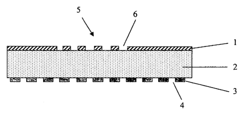
Fig. 1 shows a thin layer composition according to the invention in form of a
three-layer composition, capable of interference, of a partially transmitting
layer 1
having a gap 5 and a reflecting layer 3 having a multitude of grid-like
arranged
gaps 4. Between the partially transmitting layer 1 and the reflecting layer 3
a
dielectric layer 2 is arranged over the full area.
A viewer, which views from the side of the partially transmitting layer 1 onto
the
security element, perceives in incident light (or reflected light) in the
areas outside
the gap 5 a color tilt effect. Thereby the color of the thin layer composition
changes, for example from green to red, when tilting the security element from
green to red. In the region of the gap 5 the viewer perceives under almost all
viewing angles the color of the reflecting layer 3, for example the color
gray. In
case the gap 5 is for example configured in form of the number "50", the
viewer
sees, when tilting the security element, from almost all viewing angles the
gray
number "50", around the number "50", however, a color tilt effect from green
to
red.
The grid-like arranged gaps 4 are configured circular and/or line shaped,
wherein
the circular gaps have the diameter of 10 microns to 100 microns, preferably
of 30
microns to 50 microns, and the line shaped gaps have a width of 30 microns to
70
microns.
In contrast thereto, in transmitted light, light passes through the multitude
of the
gaps 4 of the reflecting layer 3 and through the remaining layers of the thin
film
CA 02726431 2010-11-30
- 13 -
composition, such that the viewer perceives both within and also outside the
gap
no color tilt effect, but a uniform gray area.
In case the viewer looks from the side of the reflecting layer 3 onto the
security
5 element, he perceives in incident light the light reflected from the
reflecting layer
3 and in a transmitted light the light passing through the gaps 4. Therefore
the
viewer perceives in incident light a metal like shining area and in
transmitted
light an uniformly gray area.
Depending on the configuration of the gap 5 in the partially transmitting
layer 1
also the gap 5 makes in transmitted light, viewed from the front side of the
security element, more or less an appearance. In order to prevent this, the
gap 5 is
replaced by a multitude of gaps 6 according to Fig. 2. By this the contrast
perceivable in incident light between the regions 5 and 1 is somewhat reduced,
in
return this leads to the region 5 to be outshined in transmitted light such,
that it is
not noticed anymore by the viewer.
The two embodiments according to Fig. 1 and Fig. 2 can also be modified to
this
effect, by configuring them double-sided according to Fig. 3. Herein a common
reflecting layer 3, which comprises the grid-like gaps, between the two
dielectric
layers 2 and 7. On the side of the respective dielectric layer 2 and 7, which
is
opposite to the reflecting layer 3, a partially transmitting layer 1 and 8 is
arranged,
respectively. Both partially transmitting layers 1 and 8 comprise gaps
according to
the exemplary embodiment of Fig. 2.
Herein it is particularly advantageous, that a color tilt effect is visible
from both
sides. On the other hand the partially transmitting layer 1 on the dielectric
layer 2
and the partially transmitting layer 8 on the dielectric layer 7 can be left
open with
different information. In incident light from the one side, for example, the
number
CA 02726431 2010-11-30
- 14 -
"50" appears and from the opposite side in incident light the symbol "E"
appears,
wherein the respective information disappears in transmitted light.
Without limiting the optical effect of the effect, according to Fig. 4 also
the
dielectric layer 2 can be left open at the locations, at which the partially
transmitting layer 1 has gaps. This is shown by way of example in Fig. 4 at
the
exemplary embodiment according to Fig. 2.
Fig. 5 shows a three-layer composition, capable of interference according to
Fig. 1
0 in transmitted light, viewed from the side of the reflecting layer 3. A
thin
continuous line 11 in form of a star is located within in the grid-like
arranged gaps
4 of the reflecting layer. To be effective the line has a width of 0,1mm to
5mm so
that the line is sufficiently noticeable in transmitted light. In incident
light it
cannot be noticed by a viewer, almost independent of its line width, as the
color
tilt effect noticeable in incident light between the regions of reflecting
layer over
the full area and of left open reflecting layer does practically not differ.
In
transmitted light the viewer therefore sees the star in addition to the
effects
described with respect to Fig. 1 and in incident light only the effects
described
with respect to Fig. 1 without the star.
Particularly advantageously the security element according to the invention is
combined with known optically active microstructures, as for example
diffractive
embossed holograms, Zero Order Gratings, refractive microstructures, such as
Blazed Gratings and such.
Fig. 6 shows by way of example such a combination with an embossed hologram,
wherein the following three-layer composition, capable of interference, was
chosen: a reflecting layer 3 having grid-like arranged gaps on a dielectric
layer 2
and a partially transmitting layer 1, which comprises gaps arranged grid-like
in
CA 02726431 2010-11-30
- 15 -
two regions. This composition is applied on an embossing lacquer 9 with a
diffractive embossing structure and a substrate 10.
This security feature shows from the frontside a first color tilt effect, for
example
from magenta to green, and from the backside a second color tilt effect, for
example from green to magenta. In addition to that in incident light from the
backside as well as from the front side different picture information, for
example
a "Ã"-sign and a "$"-sign, can be seen within the color layer. In transmitted
light
the color impressions then disappear completely and merely a light/dark-image
appears, for example a gray scale portrait. In addition to that a design can
be seen
from both sides, which is determined by the embossing structure.
Advantageously known hologram-design elements can be used for diffractive
embossing structures. The hologram information is from the front- and the
backside in the same way visible, however, mirror imaged to each other. In
transmitted light the hologram information disappears.
The exemplary embodiment according to Fig. 6 self evidently can also be
composed with the reverse layer sequence on the embossing layer, that means in
the sequence embossing lacquer, reflecting layer, dielectric layer and
partially
transmitting layer on the embossing lacquer 9 having a diffractive embossing
structure and the substrate 10. In the same way also an embodiment
corresponding to Fig. 3 is possible, that means, respectively, an optically
variable
thin layer element can be composed on both sides of the embossing lacquer 9.