Note: Descriptions are shown in the official language in which they were submitted.
CA 02726476 2010-11-30
WO 2009/158287 PCT/US2009/048031
1
ACTIVE THERMAL CONTROL FOR STACKED IC DEVICES
TECHNICAL FIELD
[0001] This disclosure relates to integrated circuits (ICs).
More
specifically, the disclosure relates to multi-tiered IC devices and even more
specifically
to systems and methods for active thermal control within the multi-tiered IC
devices.
BACKGROUND
[0002] In IC technology there is a need to stack chips together to
form
multi-tiered (3-D) IC devices (also referred to as multi-layered IC devices or
stacked IC
devices). One challenge that arises when chips are stacked is that thermal
conductivity
is reduced. Thus, hot spots could exist with little ability to move the heat
away from the
heat source. Because of the reduced size of stacked ICs, (substrate thickness
going from
100 microns to about 6-50 microns), the power density rises while lateral
thermal
conductivity is reduced.
[0003] One method for increasing lateral thermal conductivity is
to
increase the substrate thickness. This, in turn, negatively impacts the
desired form
factor of the stacked IC device and degrades performance.
[0004] An additional challenge exists when more than two tiers are
stacked. In such situations, the stacked IC device may contain multiple layers
of oxide,
one between each pair of stacked tiers. Oxide, being a poor thermal conductor,
adds to
the heat dissipation problem.
[0005] There are several approaches for addressing the thermal
conductivity issues. One approach positions a heat conducting layer between
the tiers.
Typically, heat conducting layers are metallic and thus could interfere with
inter-layer
electrical connections. Another approach uses Through Silicon Vias (TSVs) to
move
the heat from an inner tier to a surface tier of the stacked IC device and
then remove the
heat from the surface tier using traditional methods, such as positioning a
high thermal
conductivity material on the surface tier. Challenges arises with such a
solution. For
example, it is not always possible to position a TSV at the necessary location
because of
circuitry layout requirements in the various tiers.
[0006] Another approach is to circulate cooling material through
the
stacked IC device to cool the hot spots. A cooling circulation solution is
costly to
CA 02726476 2014-04-10
74769-3226
=
manufacture and, because of the moving liquid, requires a pumping mechanism
and tight
tolerances for liquid channels. Also, because of circuitry layout
requirements, it may not be
possible to "plumb" the device to channel the cooling material to the
necessary location. The
plumbing problem could be overcome, to some extent, by forcing cooling liquid
through the
substrate itself, but this method is not without a further set of problems and
costs.
BRIEF SUMMARY
[0007] Thermal conductivity in stacked IC devices can be improved by
constructing
one or more active temperature control devices within the stacked IC device.
In one
embodiment, the control devices are thermal electric (TE) devices, such as
Peltier devices.
The TE devices can then be selectively controlled to remove or add heat as
necessary to
maintain the stacked IC device within a defined temperature range or otherwise
bring the
stacked IC device to a desired temperature. The active temperature control
elements can be P-
N junctions created in the stacked IC device and can serve to move the heat
laterally and/or
vertically as desired.
[0007a] In one aspect, there is provided a stacked integrated circuit (IC)
device
comprising: a tier having an active layer in which active circuits are
disposed and a substrate
layer, the active layer directly on the substrate layer; and a thermal
electric (TE) device
partially disposed within the substrate layer and partially disposed within
the active layer in
which the active circuits are disposed, the TE device facilitating thermal
flow between an area
of said stacked IC device and said TE device.
[0007b] In another aspect, there is provided a stacked integrated
circuit (IC) device
comprising: first and second tiers, each of the first and second tiers having
an active layer in
which active circuits are disposed and a substrate layer on which the active
layer is directly
disposed; and at least one P-N junction partially constructed in at least one
of said substrate
layers of the tiers and partially constructed within at least one of the
active layers, said
junction operable for thermal energy transfer to/from a location in at least
one of said tiers by
selective application of current flow with respect to said junction.
CA 02726476 2014-12-03
74769-3226
2a
[0007e] In another aspect, there is provided a stacked integrated
circuit (IC) device
comprising: at least two bonded tiers, each tier containing an active layer in
which circuit
elements are disposed and a substrate layer on which the active layer is
directly disposed; and
a thermal electric (TE) device partially constructed within at least one of
said substrate layers
of the tiers and partially constructed within at least one of the active
layers, the thermal
electric (TE) device being configured for selectively heating/cooling a
particular area of one
of said tiers.
[0007d] In another aspect, there is provided a stacked integrated
circuit (IC) device
comprising: a tier having an active layer in which active circuits are
disposed and a substrate
layer on which the active layer is directly disposed; means for facilitating
thermal flow from
an area of the stacked IC device, the thermal flow means partially disposed
within the
substrate layer and partially disposed within the active layer in which the
active circuits are
disposed.
[0007e] In another aspect, there is provided a stacked integrated
circuit (IC) device
comprising: first and second tiers, each of the first and second tiers having
an active layer in
which active circuits are disposed and a substrate layer on which the active
layer is directly
disposed; and means for transferring thermal energy to/from a location in at
least one of the
tiers by selective application of current flow with respect to the
transferring means, the
transferring means partially constructed in at least one of the substrate
layers of the tiers and
partially constructed within at least one of the active layers.
1000711 In another aspect, there is provided a stacked integrated
circuit (IC) device
comprising: at least two bonded tiers, each tier containing an active layer in
which circuit
elements are disposed and a substrate layer on which the active layer is
directly disposed; and
means for facilitating thermal flow partially constructed within at least one
of the substrate
layers of the tiers and partially constructed within at least one of the
active layers, the thermal
means being configured for selectively heating/cooling a particular area of
one of the tiers.
[0007g] In another aspect, there is provided a method for controlling
undesired
temperature gradients in a stacked integrated circuit (IC), the method
comprising: allowing
CA 02726476 2014-12-03
74769-3226
2b
energy to flow between an area within the IC and a thermal electric (TE)
device, wherein the
IC includes a tier having a substrate layer and an active layer in which
active circuits are
disposed, wherein the active layer is directly disposed on the substrate
layer, and wherein the
TE device is partially disposed within the substrate layer and partially
disposed within the
active layer; and enabling current to flow with respect to the TE device so as
to selectively
control the energy flow.
[0007h] In another aspect, there is provided a method of removing heat
from a hot spot
in a multi-tiered integrated circuit (IC) device, the method comprising:
allowing heat from the
hot spot to pass through the multi-tiered IC device from one tier to at least
one other tier,
wherein the at least one other tier includes a substrate layer and an active
layer in which active
circuits are disposed, wherein the active layer is disposed directly on the
substrate layer, and
wherein a thermal electric (TE) device is partially disposed within the
substrate layer of the at
least one other tier and partially disposed within the active layer of the at
least one other tier;
and enabling the TE device to transfer the heat out of the multi-tiered IC
device.
[0008] The foregoing has outlined, rather broadly, the features and
technical
advantages of the present invention in order that the detailed description of
the invention that
follows may be better understood. Additional features and advantages of the
invention will be
described hereinafter which form the subject of the claims of the invention.
It should be
appreciated by those skilled in the art that the conception and specific
embodiment disclosed
may be readily utilized as a basis for modifying or designing other structures
for carrying out
the same purposes of the present invention. It should also be realized by
those skilled in the
art that such equivalent constructions do not depart from the scope of the
invention as set forth
in the appended claims. The novel features, which are believed to be
characteristic of the
invention, both as to its organization and method of operation, together with
further objects
and advantages, will be better understood from the following description when
considered in
connection with the accompanying figures. It is to be expressly understood,
however, that
each of the figures is provided for the purpose of illustration and
description only and is not
intended as a definition of the limits of the present invention.
CA 02726476 2010-11-30
WO 2009/158287 PCT/US2009/048031
3
BRIEF DESCRIPTION OF THE DRAWINGS
[0009] For a more complete understanding of the present invention,
reference is now made to the following descriptions taken in conjunction with
the
accompanying drawings, in which:
[0010] FIGURE 1 is a schematic drawing of a multi-tiered IC device
having a hot spot therein;
[0011] FIGURE 2 shows one example of a prior art solution for
relieving
heat from the hot spot;
[0012] FIGURE 3 shows one embodiment of a stacked IC device having
active temperature control in accordance with the teachings of the invention;
and
[0013] FIGURES 4A through 4G show one method of manufacturing a
multi-tiered IC device having active cooling capability in accordance with the
teachings
of the invention.
DETAILED DESCRIPTION
[0014] FIGURE 1 is a schematic drawing of multi-tiered IC device
10
having top tier 11 and bottom tier 12. Top tier 11 has an active circuit
(face) 102 and
substrate (back) 101. Bottom tier 12 has active circuit (face) 103 and
substrate (back)
104. Faces 102/103 contain connections 108 which serve to connect components
(or
terminals) such a component 109 on the respective tiers. These connections are
made
using connector paths, such as path 107 and a via, such as via 106
[0015] For illustrative purposes, location 110 is thermally
troubled in
this embodiment. That is, location 110 is a "hot spot" that exists, or could
exist, from
time to time in stacked IC device 10. A hot spot, in this context, means that
as stacked
IC device 10 is operating, the temperature of the area in and around location
110 can
become undesirably higher than other portions of tier 12. Because of the
stacking of tier
11 on tier 12 and, preferably, reduced thickness of each tier, the lateral
heat spread in
tier 12 is reduced. In addition, air gap 111 can be formed between the tiers
11, 12
thereby reducing thermal flow upward from the hot spot.
[0016] As discussed above, there are a number of reasons to
include
cooling functionality or structures within a stacked IC device. But there are
also reasons
for heating a stacked IC device, or portions thereof For example, when
designing an
adaptive voltage scaling circuit, it is desirable for the entire stacked IC
device to have a
CA 02726476 2010-11-30
WO 2009/158287 PCT/US2009/048031
4
uniform temperature. Thus, if there are some localized areas of a tier in the
stacked IC
device that "run hot" (i.e., not a hot spot per se, but a localized area that
operates at a
warmer temperature than other areas in a tier) it might be desirable or
necessary to heat
the cooler areas of the tier so that the stacked IC device has a relatively
constant or
uniform temperature. In some situations, initialization of a stacked IC device
to a
required temperature is desired or important. For example, sensors may need to
be hot
to operate and a TE could be used to reduce initial heating time.
[0017] Additionally, selective heating and/or cooling may be
required or
desirable in a stacked IC device. For example, selective heating or cooling or
a
combination thereof may be used to even out the temperature gradients across
silicon to
alleviate stress caused by temperature differentials in the substrate. Also,
selective
temperature control can be used to allow the stacked IC device to operate, at
least
temporarily, in temperature environments that it otherwise would not be
designed to
operate in.
[0018] FIGURE 2 shows one example of a prior art solution for
relieving
heat from hot spot 110. In this solution, TSV array 200 is positioned above
hot spot 110
so that the heat flowing from the hot spot 110 can be conducted through face
103, across
gap 111, through face 102 and out through vias 201. In addition to the thermal
conductivity problems, inherent with moving the heat through the various
layers and
gaps, in some situations circuitry or other elements, such as element 202, can
be
positioned in the heat flow path thereby reducing (and sometimes eliminating)
the
effectiveness of the TSV array 200.
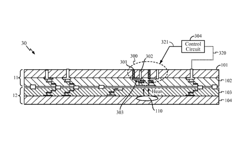
[0019] FIGURE 3 shows one embodiment of a stacked IC device 30
having active temperature control in accordance with the teachings of the
invention. A
TE device 300 includes a pair of P-N junctions. Each P-N junction includes a P-
type
element 301 and N type element 302, as well as a bottom conductor 303.
Depending on
which direction current flows through the P-N junction, the bottom conductor
303 can
either attract heat or provide heat. In one embodiment, the TE device 300 is a
Peltier
device. Although a pair of P-N junctions are shown, the invention is not
limited to such
a configuration. Rather, more or fewer P-N junctions can be provided.
[0020] Control circuit 304 is used to establish the current flow
direction
through the P-N junction. Control circuit 304 also controls current density.
Circuit 304
provides selective current control to TE device 300 via an input, such as
input 321. In
CA 02726476 2010-11-30
WO 2009/158287 PCT/US2009/048031
one embodiment, a TE device 300 operates such that a top side (top not
designated with
a reference number) heats while the other side, e.g., bottom 303, cools, based
upon the
current direction.
[0021] The thermal energy from hot spot 110 passes up through
faces
103 and 102 to device 300. This thermal flow can be facilitated by
constructing
channels (vias) through the faces if desired. By selecting the proper current
density, and
current flow direction, device 300 serves to remove heat, thereby cooling the
stacked IC
device 30. Heat sink, or other heat transfer devices, not shown, may be
located on the
surface of tier 11 adjacent to TE device 300 to assist TE device 300 in heat
removal
from stacked IC device 30. Note that the stacked IC device 30 can have TE
devices 300
provided in as many different areas as desired with some of the TE devices 300
injecting heat while others remove heat
[0022] Note that while the P-N junction material is shown going
all the
way through the substrate of tier 11, in another embodiment, the P-N material
partially
fills the substrate, with the junction being formed near the bottom conductor
303. In
this embodiment, the top portion of each via is filled by metallization,
creating a contact
within the vias.
[0023] In some embodiments, the "hot spot" can be co-located in
the
same layer as the cooling device thereby resulting in lateral heat
displacement. In such
a situation, a horizontal trench could be constructed in the substrate to
laterally transfer
the heat within the same substrate. A first portion of the trench would
include P-type
material and another portion of the trench would include N-type material.
[0024] FIGURES 4A though 4G show an exemplary method of
manufacturing a multi-layered IC device having active temperature control.
[0025] FIGURE 4A shows that tier 11 is stacked with respect to
tier 12
and that some locations, such as locations 401-405 in the substrate of tier 11
are filled
from top to bottom with sacrificial fill material. As will be seen, an active
temperature
control element will be constructed at location 400.
[0026] FIGURE 4B shows protective material 410 covering locations
401-404 in preparation for the next step in the process. Uncovered locations
405 will
become standard TSVs as the process continues.
[0027] FIGURE 4C shows the metallization of the uncovered
locations
405A by metal layer 420 to create standard TSVs 405A. Copper or any desired
metal
CA 02726476 2010-11-30
WO 2009/158287 PCT/US2009/048031
6
can be used for this purpose consistent with other elements of the stacked IC
device.
Thus, as shown in FIGURE 4C the uncovered locations now contain metal as shown
at
405A, whereas the elements 401-404 remains protected and filled with
sacrificial
material.
[0028] FIGURE 4D shows the removal of portions 410-2 and 410-4 of
protective material 410 leaving portions 410-1 and 410-3 in place. The
sacrificial
material within vias 402 and 404 is also shown removed.
[0029] FIGURE 4E shows P-type thermal electric material deposited
within locations 402 and 404. The P-type material has not been deposited
within
locations 401 and 403 because these locations remain protected by portions 410-
1 and
410-3 and thus still contain the sacrificial material.
[0030] FIGURE 4F shows the removal of portions 410-1 and 410-3 of
protective material 410 to expose vias 401 and 403. The sacrificial material
is then
removed from vias 401 and 403.
[0031] FIGURE 4G shows N-type thermal material deposited in
locations 401 and 403 thereby completing the formation of the temperature
control
device within layer 11. Typical materials for a Peltier device are bismuth
telluride,
Sb2Te3, PbTe and SiGe, but other materials, such as crystal-phonon glass or
nano
material, can be used as well. Also, it is possible to use two metals in a
metal to metal
junction such as Copper ¨ Nickel. In this embodiment, Nickel fills the TSVs
401 - 404
and Copper is the standard metallization. Accordingly, every TSV 401-404 would
be a
potential Peltier device. There are two advantages of this Peltier structure.
The first
advantage is the masking steps for P and N type fill are removed. The second
advantage
is the density of the Peltier devices is increased as one side of the TSV 401 -
404 would
act as the cooling point while the other side would be the heating side. Of
course heat
transport in the Z direction is improved while heat transfer in the X and Y
direction
becomes more difficult.
[0032] Although the description has shown the P-type material
being
deposited first and the N-type material subsequently being deposited, the
order is not
critical. That is, the N-type material could be deposited first if it is more
convenient.
[0033] It should be pointed out that the temperature differential
created
by the circuit elements in the substrate can be used to drive a voltage. The
voltage thus
created can be scavenged, for example, to drive other circuit elements as
shown by
CA 02726476 2010-11-30
WO 2009/158287 PCT/US2009/048031
7
connection 320, FIGURE 3 from control circuit 304. This would effectively
reverse the
operation of the TE device 300. The TE device 300 will cool the thermally
troubled
area (in FIGURE 3 that would be hot spot 110) because heat energy is being
removed
from the hot spot by conversion into electrical energy. The net effect then
would be that
there would be no net cooling of the stacked IC device 30 as a whole (because
energy is
being returned to the stacked IC device 30 elsewhere) but there would be
localized
cooling at the "hot spot". Consequently, overall energy savings for the
stacked IC
device 30 results.
[0034] A Peltier device is a heat pump that requires energy to
move heat
from one point to another. As the disclosed embodiments have both points
within the
system, the heat energy is being moved from a point where it is difficult to
remove
(high thermal resistance) to a location where it is easer to remove so the
heat is more
uniformly distributed within the system. Thus, the total energy demand of the
system is
increased if the Peltier device is used to move the heat. Because the TE
device can
either remove or add heat depending upon current flow direction, a device
could be used
to selectively heat or cool the stacked IC device (or a portion thereof).
[0035] In one embodiment, the Peltier device is an energy
scavenger:
some of the heat generated by the stacked IC device operation can be
recovered. The
control system can switch the Peltier device to move heat from point A to
point B
(forward bias), or point B to point A (reverse bias) or scavenge heat from a
temperature
difference between points A and B to power the system. The energy balance of
this TE
system will depend on the efficiency of the Peltier device and the duty cycle
of the
system. Thus, the Peltier device can recover some energy from the overall
system,
based upon the temperature gradient within the system. In an embodiment in
which
more than two tiers exist, stacked Peltier devices can be provided to improve
energy
scavenging efficiency. For example, a cooling Peltier device could cool one
tier,
pumping heat to an adjacent tier. The adjacent tier could use the pumped heat
to
recover additional energy.
[0036] Although the present invention and its advantages have been
described in detail, it should be understood that various changes,
substitutions and
alterations can be made herein without departing from the spirit and scope of
the
invention as defined by the appended claims. Moreover, the scope of the
present
application is not intended to be limited to the particular embodiments of the
process,
CA 02726476 2010-11-30
WO 2009/158287 PCT/US2009/048031
8
machine, manufacture, composition of matter, means, methods and steps
described in
the specification. As one of ordinary skill in the art will readily appreciate
from the
disclosure of the present invention, processes, machines, manufacture,
compositions of
matter, means, methods, or steps, presently existing or later to be developed
that
perform substantially the same function or achieve substantially the same
result as the
corresponding embodiments described herein may be utilized according to the
present
invention. Accordingly, the appended claims are intended to include within
their scope
such processes, machines, manufacture, compositions of matter, means, methods,
or
steps.