Note: Descriptions are shown in the official language in which they were submitted.
CA 02726613 2010-12-01
WO 2009/154744
PCT/US2009/003611
- 1 -
IMPROVED FORM FACTOR AND ELECTROMAGNETIC
INTERFERENCE PROTECTION FOR PROCESS DEVICE
WIRELESS ADAPTERS
BACKGROUND
In industrial settings, control systems are used to monitor and control
inventories of industrial and chemical processes, and the like. Typically, the
control system performs these functions using field devices distributed at key
locations in the industrial process and coupled to the control circuitry in
the
control room by a process control loop. Field devices generally perform a
function, such as sensing a parameter or operating upon the process, in a
distributed control or process monitoring system.
Some field devices include a transducer. A transducer is understood to
mean either a device that generates an output signal based on a physical input
or
that generates a physical output based on an input signal. Typically, a
transducer
transforms an input into an output having a different form. Types of
transducers
include various analytical equipment, pressure sensors, thermistors,
thermocouples, strain gauges, flow transmitters, positioners, actuators,
solenoids, indicator lights, and others.
Typically, each field device also includes communication circuitry that is
used for communicating with a process control room, or other circuitry, over a
process control loop. In some installations, the process control loop is also
used
to deliver a regulated current and/or voltage to the field device for powering
the
field device. The process control loop also carries data, either in an analog
or
digital format.
Traditionally, analog field devices have been connected to the control
room by two-wire process control current loops, with each device connected to
the control room by a single two-wire control loop. Typically, a voltage
differential is maintained between the two wires within a range of voltages
from
12-45 volts for analog mode and 9-50 volts for digital mode. Some analog field
CA 02726613 2014-10-09
- 2 -
devices transmit a signal to the control room by controlling the current
running
through the current loop to a current proportional to the sensed process
variable.
Other field devices can perform an action under the control of the control
room
by modulating the magnitude of the current through the loop. In addition to,
or
in the alternative, the process control loop can carry digital signals used
for
communication with field devices.
In some installations, wireless technologies have begun to be used to
communicate with field devices. Wireless operation simplifies field device
wiring and set-up. However, the majority of field devices are hardwired to a
process control room and do not use wireless conununication techniques.
Industrial process plants often contain hundreds or even thousands of
field devices. Many of these field devices contain sophisticated electronics
and
are able to provide more data than the traditional analog 4-20 mA
measurements. For a number of reasons, cost among them, many plants do not
take advantage of the extra data that may be provided by such field devices.
This has created a need for a wireless adapter for such field devices that can
attach to the field devices and transmit data back to a control system or
other
monitoring or diagnostic system or application via a wireless network.
SUMMARY
A process device wireless adapter includes a wireless communications
module, a metallic housing, and an antenna. The wireless communications
module is configured to communicatively couple to a process device and to a
wireless receiver. The metallic housing surrounds the wireless conununication
module and has a first end and a second end. The first end is configured to
attach to the process device. In one embodiment, the metallic shield contacts
the
housing second end such that the metallic shield and the housing form a
continuous conductive surface. The antenna is communicatively coupled to the
wireless communications module and separated from the wireless
communications module by the metallic shield. Preferably, the wireless
CA 02726613 2013-06-28
- 3 -
communications module illustratively includes a printed circuit board that has
a
length that is greater than its width.
According to an aspect of the present invention there is provided a
process device wireless adapter comprising:
a wireless communications module configured to communicatively
couple to a process device and to a wireless receiver;
a metallic housing that surrounds the wireless communications module,
the metallic housing having a first end and a second end, the first end
configured
to attach to the process device;
an end cap having a metallic shield that contacts the housing second end
such that the metallic shield and the housing form a substantially continuous
conductive surface; and
an antenna communicatively coupled to the wireless communications
module and separated from the wireless communications module by the metallic
shield; and
wherein the end cap comprises a non-metallic material and is configured
to attach to the housing and enclose the antenna.
According to another aspect of the present invention there is provided a
process device wireless adapter comprising:
a metallic housing having a length and a radius;
a printed circuit board within the metallic housing, the printed circuit
board having a width and a length, the length of the printed circuit board
running
along the length of the metallic housing, the length of the printed circuit
board
being greater than the width of the printed circuit board, the printed circuit
board
configured to be communicatively coupled to a process device;
an end cap having a metallic shield that forms a continuous conductive
surface with the metallic housing, the metallic shield having a first side and
a
second side, the printed circuit board positioned proximate the first side;
and
an antenna electrically connected to the printed circuit board through an
aperture in the metallic shield, the antenna positioned proximate the metallic
shield second side, the antenna configured to wirelessly transmit
communications to a wireless receiver and to wirelessly receive communications
from the wireless receiver.
CA 02726613 2013-06-28
- 3a -
According to a further aspect of the present invention there is provided a
method of improving wireless communication capabilities of a process device
comprising:
coupling a wireless communications module to the process device;
coupling an antenna to the wireless communications module;
at least partially surrounding the wireless communications module with
a conductive surface to reduce electromagnetic interference with the module;
positioning the antenna outside of the conductive surface to enable
wireless communications between the process device and a control system; and
enclosing the antenna with an end cap having a metallic shield.
According to a further aspect of the present invention there is provided a
process device wireless adapter comprising:
a wireless communications module configured to communicatively
couple to a process device and to a wireless receiver;
a metallic housing that surrounds the wireless communications module,
the metallic housing having a first end and a second end, the first end
configured
to attach to the process device;
a printed circuit board within the metallic housing, the printed circuit
board having a width and a length, the length of the printed circuit board
running
along the length of the metallic housing, the length of the printed circuit
board
being greater than the width of the printed circuit board, the printed circuit
board
configured to be communicatively coupled to a process device; and
an antenna communicatively coupled to the wireless communications
module and separated from the wireless communications module.
BRIEF DESCRIPTION OF THE DRAWINGS
FIG. 1 is a diagrammatic view of an exemplary field device with which a
wireless adapter in accordance with the present invention is useful.
FIG. 2 is a block diagram of the field device shown in FIG. 1.
FIG. 3 is a perspective view of an improved form factor wireless adapter
coupled to a process device.
FIG. 4 is a cross-sectional perspective view of the wireless adapter of
FIG. 3.
FIG. 5 is a simplified block diagram of a process control or monitoring
system that includes a wireless adapter.
CA 02726613 2013-06-28
- 3b -
FIG. 6 is a cross-sectional view of a wireless adapter that reduces or
eliminates electromagnetic interference in accordance with an embodiment of
the present invention.
FIG. 7 is a cross-sectional view of another wireless adapter that reduces
or eliminates electromagnetic interference in accordance with an embodiment of
the present invention.
FIG. 8 is a simplified cross-sectional view showing a wireless adapter
coupled to a process device.
DETAILED DESCRIPTION OF ILLUSTRATIVE EMBODIMENTS
Embodiments of the present invention generally include a wireless
adapter configured to couple to a process device and to communicate to a
process control room or a remote monitoring system or diagnostic application
running on a computer. Process devices are commonly installed in areas that
have limited access. Certain embodiments described herein include wireless
adapters having improved form factors. The improved form factors enable
wireless adapters to be coupled to process devices in a wide variety of
CA 02726613 2010-12-01
WO 2009/154744
PCT/US2009/003611
- 4 -
environments, including environments that may not otherwise allow for a
wireless adapter to be coupled to a process device. Process devices are also
commonly installed in environments having electromagnetic interference (EMI)
that may negatively impact the performance or operation of a wireless adapter.
Some embodiments described herein include wireless adapters having
electrically conductive enclosures that reduce or eliminate negative effects
from
EMI.
FIGS. 1 and 2 are diagrammatic and block diagram views of an
exemplary field device with which a wireless adapter in accordance with an
embodiment of the present invention is useful. Process control or monitoring
system 10 includes a control room or control system 12 that couples to one or
more field devices 14 over a two-wire process control loop 16. Examples of
process control loop 16 include analog 4-20 mA communication, hybrid
protocols which include both analog and digital communication such as the
Highway Addressable Remote Transducer (HART ) standard, as well as all-
digital protocols such as the FOUNDATION' m Fieldbus standard. Generally
process control loop protocols can both power the field device and allow
communication between the field device and other devices.
In this example, field device 14 includes circuitry 18 coupled to
actuator/transducer 20 and to process control loop 16 via terminal board 21 in
housing 23. Field device 14 is illustrated as a process variable generator in
that it
couples to a process and senses an aspect, such as temperature, pressure, pH,
flow, or other physical properties of the process and provides and indication
thereof. Other examples of field devices include valves, actuators,
controllers,
and displays.
Generally field devices are characterized by their ability to operate in the
"field" which may expose them to environmental stresses, such as temperature,
humidity and pressure. In addition to environmental stresses, field devices
must
often withstand exposure to corrosive, hazardous and/or even explosive
atmospheres. Further, such devices must also operate in the presence of
CA 02726613 2014-10-09
- 5 -
vibration and/or electromagnetic interference. Field devices of the sort
illustrated in FIG. 1 represent a relatively large installed base of legacy
devices,
which are designed to operate in an entirely wired manner.
FIG. 3 is a perspective view of an improved form factor wireless adapter
300 coupled to a field device 350, and FIG.4 is a cross-sectional perspective
view of adapter 300. Adapter 300 includes a mechanical attachment region 301
(e.g. a region having a threaded surface) that attaches to device 350 via a
standard field device conduit 352A. Examples of suitable conduit connections
include 1/2-14 NPT, M20x1.5, G1/2, and 3/8-18 NPT. Adapter 300 is
illustratively attached to or detached from device 350 by rotating adapter 300
about an axis of rotation 370. Attachment region 301 is preferably hollow in
order to allow conductors 344 to couple adapter 300 to device 350.
Adapter 300 includes an enclosure main body or housing 302 and end
cap 304. Housing 302 and cap. 304 provide environmental protection for the
components included within adapter 300. As can be seen in FIG. 4, housing 302
encloses or surrounds one or more wireless communications circuit boards of a
wireless communication module 310. Each circuit board is illustratively
rectangularly shaped and has a length 312 that extends along or is parallel to
axis
of rotation 370 (shown in FIG .3). Each board also has a width 314 that
extends
radially outward from or is perpendicular to axis of rotation 370.
In an embodiment, circuit board length 312 and width 314 are adjusted
or selected to enable adapter 300 to be coupled to field device 350 in a wide
variety of environments. For instance, field device 350 may be in an
environment that only has a limited amount of space for the width 314 of a
circuit board. In such a case, the width 314 of the circuit board is decreased
such
that it can fit within the environment. The length 312 of the circuit board is
correspondingly increased to compensate for the reduced width 314. This
enables the circuit board to be able to include all of the needed electronic
components while having a form factor that fits within the process device
environment. In one embodiment, length 312 is greater than width 314 (i.e. the
CA 02726613 2014-10-09
- 6 -
ratio of length to width is greater than one). Exnbodiments of the present
disclosure are not however limited to any particular ratios or dimensions. It
should also be noted that the length and/or diameter of housing 302 and cap
304
are illustratively adjusted such that the overall length and diameter/width of
wireless adapter 300 is minimized (i.e. the length and diameter of housing 302
and cap 304 are sized only as large as is needed to accommodate the enclosed
components).
FIG. 5 is a simplified block diagram of a process control or monitoring
system 500 in which a control room or control system 502 communicatively
couples to field device 350 through wireless adapter 300. Wireless adapter 300
includes a wireless communications module 310 and an antenna 320. Wireless
communications module 310 is coupled to process device controller 356 and
interacts with external wireless devices (e.g. control system 502 or other
wireless devices or monitoring systems as illustrated in FIG. 5) via antenna
320
based upon data from controller 356. Depending upon the application, wireless
communications module 310 may be adapted to communicate in accordance
with any suitable wireless communication protocol including, but not limited
to:
wireless networking technologies (such as WEE 802.11b wireless access points
and wireless networking devices built by LinkSYSTM of Irvine, California);
cellular
or digital networking technologies (such as MicroburstO by Aeris
Communications Inc. of San Jose, California); ultra wide band, free space
optics, Global System for Mobile Communications (GSM), General Packet
Radio Service (GPRS); Code Division Multiple Access (CDMA); spread
spectrum technology, infrared communications techniques; SMS (Short
Messaging Service/text messaging); a known Bluetooth Specification, such as
Bluetooth Core Specification Version 1.1 (February 22, 2001), available from
the Bluetooth SIG (www.bluetooth.com); and the Wireless HARTS
Specification published by the HART Communication Foundation, for example.
Relevant portions of the Wireless HART Specification include: HCF_Spec 13,
revision 7.0; HART Specification 65 ¨ Wireless Physical Layer Specification;
CA 02726613 2014-10-09
- 7 -
HART Specification 75 TDMA Data Link Layer Specification (TDMA refers to
Time Division Multiple Access); HARM Specification 85 ¨ Network Management
Specification; HART Specification 155 ¨ Wireless Command Specification; and
HART Specification 290 ¨ Wireless Devices Specification. Further,
known data collision technology can be employed such that multiple units can
coexist within wireless operating range of one another. Such collision
prevention can include using a number of different radio-frequency channels
and/or spread spectrum techniques.
Wireless communications module 310 can also include transducers for a
plurality of wireless communication methods. For example, primary wireless
communication could be performed using relatively long distance
communication methods, such as GSM or GPRS, while a secondary, or
additional communication method could be provided for technicians, or
operators near the unit, using for example, IEEE 802.11b or Bluetooth.
Field device 350 further includes power circuitry 352 and an
actuator/transducer 354. In one embodiment, power from power circuitry 352
energizes
controller 356 to interact with actuator/transducer 354 and wireless
communications module 310. Power from power circuitry 352 may also energize
components of wireless adapter 300. Process device controller 356 and wireless
communications module 310 illustratively interact with each other in
accordance
with a standard industry protocol such as 4-20 mA, HART , FOUNDATIONTm
Fieldbus, Profibus-PA, Modbus, or CAN. = Alternatively, the wireless adapter
may be powered by its own power source such as a battery or from other sources
such as from energy scavenging.
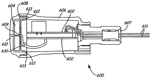
FIG. 6 is a cross-sectional view of a wireless adapter 600 that reduces or
eliminates electromagnetic interference (EMI) in accordance with an
embodiment of the present invention. Adapter 600 includes wireless
communications module electronics 602 (e.g. one or more printed circuit
boards), antenna 604, metallic housing or enclosure 606, a metallic shield
608,
non-metallic end cap 610 (e.g. a plastic radome), and a conductive elastomeric
CA 02726613 2010-12-01
WO 2009/154744
PCT/US2009/003611
- 8 -
gasket 612. Metallic enclosure 606 is illustratively made from metalized
plastic
or from a metal such as aluminum and has a cylindrical shape. Metallic shield
608 is illustratively made from a plastic plated with a conductive material or
from a metal such as stamped sheet metal.
Gasket 612 fits within an annular ring 613 of enclosure 606. Gasket 612
is in contact with both metallic enclosure 606 and metallic shield 608 such
that
the three components form a continuous conductive surface. This conductive
surface protects wireless communications module 602 from EMI.
Metallic shield 608 has a small hole or aperture 609. Aperture 609
allows for an electrical connection 630 (e.g. a coaxial cable) to pass through
shield 608 and to connect antenna 604 to wireless communications module 602.
Altematively, antenna 604 can be formed integrally with module 602, for
example in the form of traces routed around an outside edge of a circuit
board.
In such a case, the integrally formed antenna 604 is passed through shield 608
through aperture 609.
Non-metallic end cap 610 and metallic shield 608 surround antenna 604
and provide physical protection (e.g. environmental protection) for the
antenna.
Wireless signals are able to pass through non-metallic end cap 610. This
allows
for antenna 604 to transmit and receive wireless signals. In an embodiment,
shield 608 and antenna 604 are designed such that shield 608 is part of the
ground plane of antenna 604.
Metallic enclosure 606 has a small hole or aperture 607. Aperture 607
allows for electrical conductors or connections 611 to pass through.
Connections
611 illustratively couple wireless adapter 600 to a process device such that
communication signals may be transferred between wireless adapter 600 and the
process device. Adapter 600 illustratively communicates with a process device
in accordance with an industry protocol, such as those set forth above (e.g.
HART ). Connections 611 may also supply wireless adapter 600 with electrical
power (e.g. current or voltage).
CA 02726613 2013-06-28
- 9 -
FIG. 7 is a cross-sectional view of another wireless adapter 700 that
reduces or eliminates EMI in accordance with an embodiment of the present
invention. Adapter 700 includes many of the same or similar components as
adapter 600 and is numbered accordingly. Adapter 700 includes an antenna 704,
an
end cap 710, connections 711 and electrical connection 730. Adapter 700 does
not
include a conductive gasket like adapter 600. Instead, metallic shield 708 has
electrically conductive tabs or spring fingers 718. Fingers 718 fit within the
enclosure annular ring 712 such that shield 708 and enclosure 706 form a
continuous
conductive surface that surrounds wireless communications module 702. The
surrounding conductive surface protects electronics within module 702 from
EMI.
In another embodiment of a wireless adapter, the electronics enclosure
(e.g. enclosure 606 in FIG. 6 and enclosure 706 in FIG. 7) is made from a non-
metallic material. The wireless adapter communications electronics (e.g.
module
602 in FIG. 6 and module 702 in FIG. 7) are illustratively protected from EMI
by a separate metallic shield that is within the electronics enclosure and
that
surrounds the electronics.
In yet another embodiment of a wireless adapter, the adapter does not
include an end cap (e.g. end cap 610 in FIG. 6) that encloses an antenna.
Instead,
a "rubber duck" style whip antenna is used. The whip antenna is positioned or
placed adjacent to the adapter shield (e.g. shield 608 in FIG. 6) and is left
exposed to the environment.
= Wireless adapters are illustratively made =to meet intrinsic safety
requirements and provide flame-proof (explosion-proof) capability.
Additionally, wireless adapters optionally include potting within their
electronic
enclosures to further protect the enclosed electronics. In such a case, the
metallic
shields of the wireless adapters may include one or more slots and/or holes to
facilitate potting flow.
FIG. 8 is a cross-sectional view of wireless adapter 800 coupled to a
process device 850, in accordance with one embodiment of the present
invention. Device 850 includes an actuator/transducer 864 and measurement
CA 02726613 2013-06-28
- 10 -
circuitry 866.Measurement circuitry 866 couples to field device circuitry 868.
Device 850 couples to two-wire process control loop 888 through a connection
block 806 and wireless adapter 800. Further, wireless adapter 800 couples to
the
housing of device 850. In the example shown in FIG. 8, the coupling is through
an NPT conduit connection 809. The chassis of wireless adapter 800
illustratively couples to an electrical ground connection 810 of device 850
through wire 808. Device 850 includes a two-wire process control loop
connection block 802 which couples to connections 812 from wireless adapter
800. As illustrated in FIG. 8, wireless adapter 800 can be threadably received
in
conduit connection 809. Threads 822 are shown in FIG .8. Housing 820 carries
antenna 826
to support circuitry of wireless adapter 800. Further, an end cap 824 can be
sealably coupled
to housing 820 and allow transmission of wireless signals therethrough. Note
that
in the arrangement shown in FIG. 8, five electrical connections are provided
to
wireless adapter 800 (i.e. four loop connections and an electrical ground
connection). These electrical and mechanical connection schemes are however
for illustration purposes only. Embodiments of the present invention are not
limited to any particular electrical or mechanical connection scheme, and
embodiments illustratively include any electrical or mechanical connection
scheme.
The term "field device" as used herein can be any device which is used
in a process control or monitoring system and does not necessarily require
placement in the "field." Field devices include, without limitation, process
variable transmitters, digital valve controllers, flowmeters, and flow
computers.
The device can be located anywhere in the process control system including in
a
control room or control circuitry. The terminals used to connect to the
process
control loop refer to any electrical connection and may not comprise physical
or
discrete terminals. Any appropriate wireless communication circuitry can be
used as desired as can any appropriate communication protocol, frequency or
communication technique. Power supply components are configured as desired
and are not limited to the configurations set forth herein or to any other
CA 02726613 2010-12-01
WO 2009/154744
PCT/US2009/003611
- 11 -
particular configuration. In some embodiments, the field device includes an
address which can be included in any transmissions such that the device can be
identified. Similarly, such an address can be used to determine if a received
signal is intended for that particular device. However, in other embodiments,
no
address is utilized and data is simply transmitted from the wireless
communication circuitry without any addressing information. In such a
configuration, if receipt of data is desired, any received data may not
include
addressing information. In some embodiments, this may be acceptable. In
others, other addressing techniques or identification techniques can be used
such
as assigning a particular frequency or communication protocol to a particular
device, assigning a particular time slot or period to a particular device or
other
techniques. Any appropriate communication protocol and/or networking
technique can be employed including token-based techniques in which a token is
handed off between devices to thereby allow transmission or reception for the
particular device.
As has been discussed, embodiments of the present invention improve
wireless communications with a process device. Certain embodiments reduce
electromagnetic interference with wireless adapters by providing a conductive
surface that surrounds and protects the enclosed electrical communications
modules or components. Antennas of wireless adapters are illustratively placed
outside of the conductive surface such that they can communicate wirelessly
with a control system. Antennas are optionally environmentally protected by
enclosing the antennas with a non-metallic end cap that allows wireless
signals
to pass through. Additionally, embodiments include improved form factors that
enable wireless adapters to be attached to process devices that are in
confined
environments that may not otherwise permit attachment of a wireless adapter.
The form factors are illustratively improved by reducing a width of the
wireless
adapter and compensating for the width reduction by increasing a length of the
adapter.
CA 02726613 2014-10-09
- 12 -
Although the present invention has been described with reference tó
particular embodiments, workers skilled in the art will recognize that changes
may be made in form and detail without departing from the scope of the
invention.