Note: Descriptions are shown in the official language in which they were submitted.
CA 02726986 2010-12-03
WO 2009/149062 PCT/US2009/045933
ANNEALING OF SEMI-INSULATING CdZnTe CRYSTALS
BACKGROUND
[0001] Field of the Invention
[0002] The present invention relates to Cd1_,tZn,;Te samples/wafers and, more
particularly, to a method of annealing Cd1.,Zn,Te samples/wafers.
[0003] Description of Related Art
[0004] Semi-insulating Cdl-xZn,,Te crystals with a Zn composition typically in
the 0 <_ x<_
0.25 mole fraction range are typically used for room-temperature semiconductor
x-ray and
ganmmma-ray radiation detector applications. The semi-insulating or high
electrical resistivity
(> 1.09 f2cm) state of such Cdi-,;ZnTe crystals is typically achieved by a
deep-level defect
compensation technique. While achieving the highly resistive state is
straightforward with
this technique, it is not trivial and very challenging to keep the
concentration of the
electrically active compensating deep-level defects sufficiently low to
achieve good carrier
lifetimes and mobilities.
[0005] The product of electron (e) and hole (h) mobilities (p) and lifetimes (-
r) ( j, and
phti11 respectively) are key material parameters controlling the performance
of x-ray and
gamma-ray detectors fabricated from semi-insulating Cdi-,Zn,,Te crystals. In
order to achieve
the necessary high electron and hole mobility lifetime products, Cdi_xZn"Te
ingots and
crystals are typically subjected to annealing (heat treatment) in-situ in the
growth ampoule
(essentially during the cool down of the as-grown ingot) or ex-situ in a post-
growth annealing
process, typically after the crystals are separated by slicing and dicing. The
annealing process
either relaxes the defect structure of the crystals or ingots (essentially
reduces the
concentration of harmful defects) or passivates the electrically active
defects (no change in
the defect concentration but reduction of the active fraction of the defects).
[0006] Notwithstanding the success of current methods of annealing semi-
insulating Cd1
,tZnxTe crystals, it would be beneficial for room-temperature semiconductor x-
ray and
gamma-ray radiation detector applications to provide semi-insulating Cd1-
,Zn;tTe crystals that
have even better electron and hole mobility lifetime product.
SUMMARY OF THE INVENTION
[0007] The invention is a method of annealing a Cd1-,,Zn Te sample/wafer
comprises (a)
removing surface contamination from the sample/wafer; (b) installing the
sample/wafer of
step (a) into a chamber; (c) following step (b), evacuating the chamber; (d)
introducing
-1-
CA 02726986 2010-12-03
WO 2009/149062 PCT/US2009/045933
Hydrogen or Deuterium gas into the evacuated chamber; (e) heating the
sample/wafer to a
suitable annealing temperature; and (f) maintaining the sample/wafer in the
conditions of
steps (d) and (e) for a predetermined period of time.
[0008] Step (e) can include heating the sample/wafer to a temperature between
400 C -
650 C.
[0009] The method can further include, prior to step (c), installing Tellurium
in the
chamber. Step (e) can further include heating the evacuated chamber whereupon
the
sample/wafer in the chamber is at a higher temperature than the Tellurium in
the chamber.
[0010] The sample/wafer can be heated to a temperature between 400 C - 650 C.
The
Tellurium can be heated to a temperature between 250 C - 550 C.
[0011] The predetermined period of time can be between 1 hour and 128 days.
[0012] The Zn composition of the Cdl_,;Zn,,Te sample/wafer is between 0 ~x
X0.25 mole
fraction.
[0013] The method can further include: (g) following step (f), cooling the
chamber to
room temperature at a rate between 0.01 degree centigrade per minute and 1.0
degree
centigrade per minute; (h) following step (g), removing the sample/wafer from
the chamber;
and (i) fabricating the removed sample/wafer into one or more x-ray and/or
gamma-ray
radiation detectors.
[0014] Between 0.1 - 1.0 atmosphere of Hydrogen or Deuterium gas can be
introduced
into the evacuated chamber.
[0015] The invention is also a method of annealing a Cdi_XZnTe sample/wafer
comprising: (a) exposing the sample/wafer to pressure of ~ 10-5 torn of
ambient air; (b)
following step (a), exposing the sample/wafer to X1.0 atmosphere of Hydrogen
or Deuterium
gas; (c) heating the sample/wafer to an annealing temperature; (d) maintaining
the
sample/wafer in the conditions of steps (b) and (c) for a predetermined period
of time.
10016] Step (c) can include heating the sample/wafer to a temperature between
400 C -
650 C.
[0017] The method can further include exposing the sample/wafer to between 2.1
x 10-7
and 3.0 x 10⁻³ atmospheres of Tellurium vapors. Step (c) can further include
heating the
sample/wafer to a temperature greater than a temperature of a source of the
Tellurium vapors.
[00181 The source of the Tellurium vapors can be heated to a temperature
between 250 C
- 550 C.
[0019] The method can further include: (e) following step (d), cooling the
sample/wafer
to room temperature at a rate between 0.01 degree centigrade per minute and
1.0 degree
-2-
CA 02726986 2010-12-03
WO 2009/149062 PCT/US2009/045933
centigrade per minute; (f) following step (e), exposing the sample/wafer to
ambient air and
pressure; and (g) fabricating the removed sample/wafer into one or more x-ray
and/or
gamma-ray radiation detectors.
[0020] The method can further include, prior to step (a), removing surface
contamination
from the sample/wafer.
10021] The predetermined period of time can be between 1 hour and 128 days.
BRIEF DESCRIPTION OF THE DRAWING
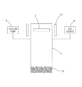
10022] Fig. 1 is a schematic view of an annealing chamber for annealing
samples/wafers
in accordance with the present invention.
DETAILED DESCRIPTION OF THE INVENTION
[00231 Disclosed is an annealing process for semi-insulating Cdl_,ZnTe
crystals in the
presence of Hydrogen (H2) gas; Hydrogen (H2) gas and Tellurium (Te2) vapors;
Deuterium
(D2) gas; or Deuterium (D2) gas and Tellurium (Te2) vapors that increases the
electron
mobility-lifetime product of the crystals, typically by a factor of 2x - 5x,
depending on the
process parameters utilized to grow the crystals and the annealing process
parameters. This
increase in the electron mobility-lifetime product of the crystals results in
improvements in
both the performance of x-ray and gamma-ray detector devices made from the
crystals as
well as the fabrication yields of the crystals. The annealing process is not
limited by the size
or geometry of the devices or the composition (x) of the Cdl-XZnxTe crystals.
[0024] With reference to Fig. 1, in preparation for annealing, Cdl-KZn,,Te
crystal boules
are formed into samples/wafers (slices) 2 of desired size and thickness.
Surface
contamination is then removed from each sample/wafer 2 by any suitable and/or
desirable
cleaning technique known in the art, e.g., chemical etching, plasma cleaning,
etc. One or
more sample(s)/wafer(s) 2 are then placed in an annealing chamber 4, e.g.,
without limitation,
a quartz annealing tube. Chamber 4 is then evacuated via a vacuum pump 6 to a
high
vacuum, e.g., without limitation, less than 10-5 torr, to remove atmospheric
(ambient) air and
its water vapor from the interior of chamber 4. Once evacuated, the interior
of chamber 4 is
then filled with 0.1-1.0 atm high-purity Hydrogen (H2) gas, or alternatively,
with high purity
Deuterium (D2) gas from a gas source 8 and sealed vacuum tight. Optionally,
prior to
chamber 4 being evacuated to a high vacuum, an appropriate size load of high-
purity Te 10 is
introduced into chamber 4 at a different location than the sample(s)/wafer(s)
2 to enable a
temperature difference to be formed between the Cdl_,,Zn,,Te
sample(s)/wafer(s) 2 and the Te
-3-
CA 02726986 2010-12-03
WO 2009/149062 PCT/US2009/045933
charge. For the purpose of this description, it will be assumed that To is
present in the
chamber. However, this is not to be construed as limiting the invention since
it is envisioned
that annealing of the sample(s)/wafer(s) 2 (described hereinafter) can be
accomplished only
in the presence of Hydrogen (H2) or Deuterium (D2) gas.
10025] Chamber 4 is then heated via a suitable heating means, such as, without
limitation,
a resistive heater 12, to desired temperatures whereupon a temperature
gradient forms in
chamber 4 such that the temperature of the sample(s)/wafer(s) 2, or the
annealing temperature
(Tana), is higher than the temperature of the Te vapor source (TTe). The
partial pressure of
vapors of Te, i.e., Tee, in chamber 4 (when To is provided in chamber 4) has
been observed to
be between 2.1 x 10-" atm and 3.0 x 10'3 atm. Suitable temperature ranges of
Taõn and TTe
include: Tanõ = 400 C - 650 C and TT, = 250 C - 550 C. The sample(s)/wafer(s)
2 are
annealed under these conditions for a period typically between 1 hour and 128
days
depending on the thickness of the sanpl.e(s)/wafer(s) 2 to achieve an increase
of the electron
mobility-lifetime product.
[0026] Once annealing of the sample(s)/wafer(s) 2 is complete, chamber 4 is
cooled to
room temperature at a cooling rate that is desirably between 1.0 C /minute
and 0.01
C/minute. The cool-down of the sample(s)/wafer(s) 2 may be interrupted by one
or more
equilibrium stages where the temperature inside chamber 4 is caused to remain
constant for a
desired period of time. The sample(s)/wafer(s) 2 are then unloaded from the
chamber 4 and
fabricated into x-ray and gamma-ray radiation detector devices.
[00271 In a deep donor compensation scheme, the point-defect controlled matrix
electron.
eT,, product can be increased in two ways: (1) The shallow donor concentration
increases
and/or (2) the shallow acceptor concentration decreases. A modification of the
deep donor
concentration only leads to changes of the resistivity and the hole hxh
product. The reason
for is that the concentration of the ionized the deep donors, which determines
the electron
ie' e product, has to balance the shallow donor - shallow acceptor
compensation offset within
<10-6 ppb to maintain high resistivity at RT (e.g., >l09 S2cm). Hence, if the
shallow level
concentrations are constant, possible variations of the ionized deep donor
concentrations are
orders of magnitude too small to affect the electron !.e'ce product.
[00281 In a deep acceptor compensation scheme, the point-defect controlled
matrix
electron ~vc product can be increased in three ways: (1) The shallow donor
concentration
increases and/or (2) the shallow acceptor concentration decreases and/or (3)
the deep acceptor
-4-
CA 02726986 2010-12-03
WO 2009/149062 PCT/US2009/045933
concentration decreases. The third option is added because in a deep acceptor
scheme, the
electron t product is determined by the concentration of the neutral deep
acceptors.
[0029] It is believed that the diffusing species (H2; D2; Te; H2 and Te; or D2
and Te)
modify one or more of those principal defect concentrations by (a)
adding/eliminating defects
and/or (b) passivating/de-passivating defects, i.e., making the defects
electrically
inactive/active (includes possible complex formation/dissolution) and/or (c)
modifying deep
level capture cross sections for electrons and/or (d) changing defect energy
levels by complex
formation (shallow-deep or deep-shallow conversion).
[0030] In Cdl-XZn,Te crystals vastly different shallow donor concentrations
(typically but
not limited to 200 ppb - 3,000 ppb) can lead to almost complete shallow level
compensation,
i.e., NAS-NDSI < 0.1 ppb, where NAS and NDS are the concentrations of shallow
acceptors and
shallow donors, respectively. This estimate is based on the maximum ionized
(deep donor
compensation scheme) or neutral (deep acceptor compensation scheme) deep level
defect
concentration allowed to yield iete >10-3 em2/V. Possible processes involving
larger changes
of defect concentrations may occur but have to be buffered by a self driven
mechanism (self
compensation). Also, typical SIMS detection limits for H2 and D2 in
Cdl_,,Zn,,Te crystals are
1500 ppb and 20 ppb, respectively and Te is a matrix component, i.e., actual
modifications of
defect concentrations in the relevant (sub-ppb) range are not easily mass
spectroscopically
traceable and the foregoing explanations have to be considered speculative at
this point.
[00311 One characteristic of the annealing process is that in parallel with
the increase of
the electron mobility-lifetime product by a factor of 2x - 5x, the electrical
resistivity of the
crystals decreases by the same factor 2x - 5x.
[0032] Experiments show that the foregoing annealing process produces a
desired
increase in the electron mobility-lifetime product for a wide range of
experimental
conditions, such as: annealing temperature(s); Te reservoir temperature(s) (if
Te is included
in the chamber); and Hydrogen and Deuterium pressures.
[0033] The invention has been described with reference to the preferred
embodiment(s).
Obvious modifications and alterations will occur to those of ordinary skill in
the art upon
reading and understanding the preceding detailed description. It is intended
that the invention
be construed as including all such modifications and alterations insofar as
they come within
the scope of the appended claims or the equivalents thereof.
-5-