Note: Descriptions are shown in the official language in which they were submitted.
CA 02727268 2010-12-08
WO 2010/002632 PCT/US2009/048248
-1 -
SYSTEM AND METHOD TO FABRICATE MAGNETIC RANDOM ACCESS
MEMORY
L Field
[0001] The present disclosure is generally related to fabricating magnetic
random
access memory.
IL Description ofRelated Art
[0002] Advances in technology have resulted in smaller and more powerful
computing
devices. For example, there currently exist a variety of portable personal
computing
devices, including wireless computing devices, such as portable wireless
telephones,
personal digital assistants (PDAs), and paging devices that are small,
lightweight, and
easily carried by users. More specifically, portable wireless telephones, such
as cellular
telephones and Internet Protocol (IP) telephones, can communicate voice and
data
packets over wireless networks. Further, many such wireless telephones include
other
types of devices that are incorporated therein. For example, a wireless
telephone can
also include a digital still camera, a digital video camera, a digital
recorder, and an
audio file player. Also, such wireless telephones can process executable
instructions,
including software applications, such as a web browser application, that can
be used to
access the Internet. As such, these wireless telephones can include
significant
computing capabilities.
[0003] Reducing power consumption has led to smaller circuitry feature sizes
and
operating voltages within such portable devices. Reduction of feature size and
operating voltages, while reducing power consumption, also increases
sensitivity to
noise and to manufacturing process variations.
[0004] Memory is typically included in wireless devices, and power consumption
may
be reduced through reduction of memory power requirements. Magnetic Random
Access Memory (MRAM) may consume less power than other types of memory, and
may be desirable for use in wireless devices. Fabrication techniques that
increase
effectiveness of MRAM devices by decreasing power consumption or increasing
reliability with reduced feature size are therefore desirable.
CA 02727268 2010-12-08
WO 2010/002632 PCT/US2009/048248
-2-
M Summary
[0005] In a particular embodiment, a method of aligning a magnetic film is
disclosed.
The method includes applying a first magnetic field during a deposition of a
first
magnetic material onto a substrate and applying a second magnetic field along
a second
direction in the region concurrently during the deposition onto the substrate.
[0006] In another particular embodiment, an apparatus is disclosed. The
apparatus
includes a deposition chamber configured to deposit a magnetic material onto a
substrate. The deposition chamber includes a deposition region. The apparatus
also
includes means for applying a first magnetic field within the deposition
region, the first
magnetic field oriented substantially along a first direction. The apparatus
further
includes means for applying a second magnetic field within the deposition
region, the
second magnetic field oriented substantially along a second direction.
[0007] In another particular embodiment, the apparatus includes a housing
defining an
enclosure configured to enclose a substrate including a first substrate
portion having a
first easy axis and a second substrate portion having a second easy axis. The
substrate
is to receive a magnetic material via deposition while the substrate is in the
enclosure.
The apparatus further includes a first magnetic field generator configured to
generate a
first magnetic field in the enclosure. The first magnetic field has a first
magnetic field
direction. The apparatus also includes a second magnetic field generator
configured to
generate a second magnetic field in the enclosure. The second magnetic field
has a
second magnetic field direction. When the first magnetic field direction
substantially
coincides with the first easy axis, a first portion of the deposited magnetic
material
residing on the first substrate portion has a first magnetic orientation that
is at least
partially aligned with the first easy axis. When the second magnetic field
substantially
coincides with the second easy axis, a second portion of the deposited
magnetic material
residing on the second substrate portion has a second magnetic orientation
that is at least
partially aligned with the second easy axis.
[0008] In another particular embodiment, a magnetic random access memory
(MRAM)
is disclosed. The MRAM includes a substrate including a first substrate
portion having
a first easy axis and a second substrate portion having a second easy axis.
The MRAM
also has a film that includes magnetic material deposited on the substrate.
The film
CA 02727268 2010-12-08
WO 2010/002632 PCT/US2009/048248
-3-
includes a first film portion and a second film portion. The first film
portion is coupled
to the first substrate portion, and the first film portion includes a first
magnetic material
portion that is aligned substantially along the first easy axis. The film also
includes a
second film portion coupled to the second substrate portion. The second film
portion
includes a second magnetic material portion that is substantially aligned with
the second
easy axis. During deposition of the film, the substrate is subjected to a
first magnetic
field that is oriented substantially along the first easy axis while the
substrate is also
subjected to a second magnetic field that is oriented substantially along the
second easy
axis.
[0009] A Tunnel Magnetoresistant Ratio (TMR) is a measure of a difference in
resistances of a Magnetic Tunnel Junction (MTJ) between a "0" state and a "1"
state
stored in the MTJ within an MRAM. The larger the TMR, the more definitive the
transition between states and the less current that may be needed to write
data to an MTJ
of an MRAM. One particular advantage provided by at least one of the disclosed
embodiments is that an MRAM that incorporates one or more MTJs fabricated
according to one or more of the disclosed embodiments may exhibit lower power
consumption due to an increased TMR of some or all of the MTJs within the
MRAM.
[0010] Other aspects, advantages, and features of the present disclosure will
become
apparent after review of the entire application, including the following
sections: Brief
Description of the Drawings, Detailed Description, and the Claims.
IV. Brief Description of the Drawings
[0011] FIG. 1 is a diagram of a particular illustrative embodiment of an
apparatus to
deposit a magnetic film;
[0012] FIG. 2 is a diagram of a particular illustrative embodiment depicting
deposition
of a magnetic film that forms a portion of a magnetic random access memory;
[0013] FIG. 3A is a diagram of another particular illustrative embodiment
depicting
deposition of a magnetic film that forms a portion of a magnetic random access
memory;
CA 02727268 2010-12-08
WO 2010/002632 PCT/US2009/048248
-4-
[00141 FIG. 3B is a diagram of another particular illustrative embodiment
depicting
deposition of a magnetic film that forms a portion of a magnetic random access
memory;
[0015] FIG. 4A is a diagram of another particular illustrative embodiment of a
magnetic
film on a substrate that forms a portion of a magnetic random access memory;
[0016] FIG. 4B is a diagram of a particular illustrative embodiment of a
portion of a
magnetic random access memory;
[0017] FIG. 5A is a diagram of another particular illustrative embodiment of a
portion
of a magnetic random access memory;
[0018] FIG. 5B is a diagram of another particular illustrative embodiment of a
portion
of a magnetic random access memory;
[0019] FIG. 6 is a diagram of another particular illustrative embodiment of an
apparatus
to deposit a magnetic film; and
[0020] FIG. 7 is a flow diagram of a particular embodiment of a method of
fabricating a
magnetic random access memory.
V. Detailed Description
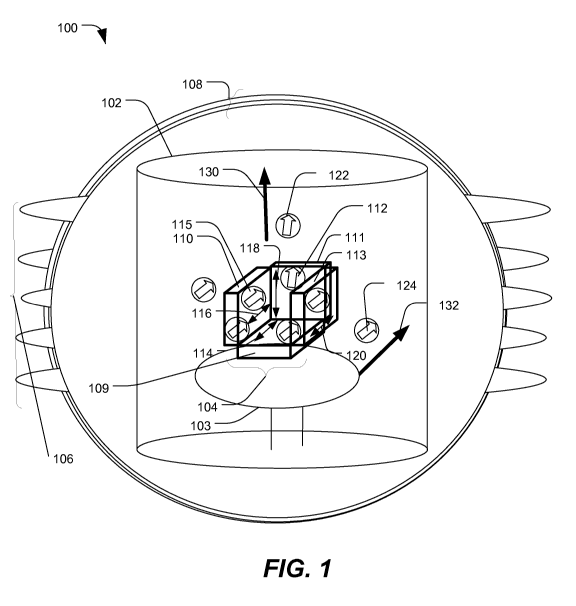
[0021] Referring to FIG. IA, a diagram of a particular illustrative embodiment
of an
apparatus to deposit a magnetic film is depicted and generally designated 100.
The
apparatus includes a deposition chamber 102 defining an enclosure in which
deposition
of a magnetic material may occur. The deposition chamber 102 is encircled by a
first
coil 106 having a first orientation and made of an electrically conducting
material. The
deposition chamber 102 is also encircled by a second coil 108 having a second
orientation and made of the same electrically conducting material or another
electrically
conducting material. An object 104 on which a first magnetic material may be
deposited may be placed within the enclosure defined by a trench in a
substrate. The
substrate may be supported within the deposition chamber 102 by a support
chuck plate
103. In a particular illustrative embodiment, the object 104 includes a first
wall 109, a
second wall 110, a third wall 111, and a fourth wall 113. In a particular
illustrative
embodiment, prior to placement in the deposition chamber 102, the object 104
has been
CA 02727268 2010-12-08
WO 2010/002632 PCT/US2009/048248
-5-
fabricated with each wall formed by the trench. Each wall of the object 104
has an easy
axis associated with the corresponding pinned magnetic layer and each easy
axis may
have an orientation associated with a corresponding wall geometry. In an
illustrative
example, a wall that is a rectangle may have an easy axis that is oriented
along a major
axis of the rectangle. For example, the first wall 109 has an easy axis 114,
the second
wall 110 has an easy axis 116, the third wall 111 has an easy axis 118, and
the fourth
wall 113 has an easy axis 120.
[0022] The first coil 106 may produce a first magnetic field 130. The second
coil 108
may produce a second magnetic field 132. In a particular illustrative
embodiment, the
first magnetic field 130 is approximately perpendicular to the second magnetic
field
132. In another particular illustrative embodiment, the first magnetic field
130 may be
at an oblique angle with respect to the second magnetic field 132.
[0023] The first coil 106 may produce the first magnetic field 130 when a
first electrical
current (not shown) passes through the coil 106, and the second coil 108 may
produce
the second magnetic field 132 when a second electrical current (not shown)
passes
through the second coil 108. In another particular illustrative embodiment,
the first
magnetic field 130 or the second magnetic field 132 may be provided by
permanent
magnets, which may be arranged in a ring or other structure surrounding the
deposition
chamber 102. In yet another particular illustrative embodiment, the first
magnetic field
130 or the second magnetic field 132 may be provided through use of an
alternative type
of magnetic field generating apparatus.
[0024] In a particular illustrative embodiment, each magnetic field may be
localized
spatially within the deposition chamber 102.
[0025] In operation, the deposition chamber 102 may contain magnetic particles
in a
gaseous state to be deposited on the walls of the object 104. The magnetic
particles may
include an illustrative magnetic particle 122 that may have a first magnetic
orientation
that is substantially aligned with the first magnetic field 130, and a second
illustrative
magnetic particle 124 that may have a second magnetic orientation that is
substantially
aligned with the second magnetic field 132.
[0026] In a particular illustrative embodiment, prior to deposition of
magnetic particles,
the object 104 may be positioned within the deposition chamber 102 with the
easy axis
CA 02727268 2010-12-08
WO 2010/002632 PCT/US2009/048248
-6-
118 substantially aligned to the first magnetic field 130 and where the third
wall 111 is
situated in a first region in which the first magnetic field 130 is present.
The object 104
may also be positioned with the easy axes 114, 116 and 120 substantially
aligned along
the second magnetic field 132 and the first wall 109, the second wall 110 and
the fourth
wall 114 situated within a second region in which the second magnetic field
132 is
present. Alternatively, the first magnetic field 130 may be oriented
approximately
parallel to the easy axis 118. Further, the second magnetic field 132 may be
oriented
approximately parallel to the easy axes 114, 116, and 120.
[0027] The first magnetic field 130 and the second magnetic field 132 may be
applied at
approximately the same time, or the first magnetic field 130 and the second
magnetic
field 132 may be applied during a common time interval. As the magnetic
particles
settle on surfaces of the object 104, each magnetic particle may be aligned
along the
corresponding easy axis of the wall upon which it settles due to the presence
of the first
magnetic field 130 or the second magnetic field 132. Prior to magnetic
material
deposition, paramagnetic conduct materials are deposited. The paramagnetic
conduct
materials lead to magnetic field aligning with layer direction. This enhances
same
magnetic field alignment particles binding with easy axis of a corresponding
wall. For
example, a first magnetic particle 112 that is subject to the first magnetic
field 130 may
be aligned along the easy axis 118 as it adheres to the third wall 111. A
second
magnetic particle 115 that is subject to the second magnetic field 132 may be
aligned
along the easy axis 116 as it adheres to the second wall 110. Magnetic
alignment of
deposited magnetic particles substantially along an easy axis of a wall may
result in an
increased Tunnel Magnetoresistant Ratio (TMR) of the fabricated MTJ. When
incorporated into an MRAM, MTJs fabricated using the deposition method
described
herein (three dimension) may result in lower power consumption and higher MTJ
density of the resulting MRAM in comparison with MRAMs that are made with MTJs
fabricated by other methods (e.g. one dimension).
[0028] In another particular illustrative embodiment, the first magnetic field
130 and the
second magnetic field 132 may have a substantially uniform field strength
throughout a
portion of the deposition chamber. In this case, magnetic particles being
deposited may
tend to align along a resultant magnetic field that is a vector sum of the
first magnetic
field 130 and the second magnetic field 132. The magnetic particles deposited
onto the
CA 02727268 2010-12-08
WO 2010/002632 PCT/US2009/048248
-7-
walls of the object 104 may be aligned along the vector sum of the first
magnetic field
130 and the second magnetic field 132, and each deposited magnetic particle
may be at
least partially aligned with the corresponding easy axis of the wall on which
the
magnetic particle is deposited.
[0029] Referring to FIG. 2, a diagram of a particular illustrative embodiment
depicts
deposition of a magnetic film, including a first magnetic material, to form a
portion of a
magnetic random access memory generally designated 200. A substrate 202
includes a
second magnetic material that has a substantially fixed orientation within the
substrate
202. The second magnetic material within the substrate 202 may be referred to
as
"pinned" in orientation (also "pinned layer" herein).
[0030] During deposition, exposed surfaces of the substrate 202 become coated
with
magnetic particles. The deposition chamber may deposit magnetic materials
through
physical vapor deposition, plasma enhanced physical vapor deposition, or via
another
means of material deposition. As magnetic particles are deposited on the
substrate 202,
the magnetic particles form a magnetic film 208 that may include many
molecular
thicknesses of magnetic particles. The magnetic particles that are deposited
may have
random magnetic orientations. An arrow 206 represents an easy axis of the
substrate,
which is a preferred direction of orientation associated with the substrate
shape and a
pinned magnetic layer within the substrate 202. As a result of the random
orientations
of the deposited magnetic particles, there is typically no magnetic alignment
of the
deposited magnetic particles along the easy axis 206 of the substrate 202.
[0031] Referring to FIG. 3A, a diagram of another particular illustrative
embodiment
depicting deposition of a magnetic film that forms a portion of a magnetic
random
access memory is depicted. A substrate 302 has been placed into a deposition
chamber
to receive magnetic particles that forma magnetic film 310 on the substrate
302. The
deposition chamber (not shown) may deposit the magnetic particles via physical
vapor
deposition, plasma enhanced physical vapor deposition, or via another means. A
magnetic field 308, which is typically of low intensity, e.g., less than 100
Oersted, may
be applied during deposition to the space within the deposition chamber.
Magnetic
particles, such as magnetic particle 306, may become aligned along a direction
of an
applied magnetic field 308 during deposition while in the presence of the
magnetic field
308. The substrate 302 may have an easy axis 304. Prior to deposition, the
substrate
CA 02727268 2010-12-08
WO 2010/002632 PCT/US2009/048248
-8-
302 may be positioned so that the easy axis 304 is aligned with the magnetic
field 308.
During deposition the magnetic particles may align themselves substantially
along a
direction of the magnetic field 308, which is parallel to the easy axis 304.
The magnetic
particles deposited on the substrate 302 form the magnetic film 310, which may
have an
average magnetic orientation 312 of the magnetic particles within the magnetic
film
310. An angle of deviation 314 represents a deviation in direction of the
average
magnetic orientation 312 from the easy axis 304. As a result of applying the
low
intensity magnetic field 308 during deposition, the angle of deviation 314 may
be small,
indicative of substantial alignment of the average magnetic orientation 312
and the easy
axis 304. Thus, as a result of the low intensity magnetic field 308 during
deposition, the
magnetic film 310 is closely aligned with the easy axis 304 of the substrate
302.
Alignment may result in an increased Tunnel Magnetoresistant Ratio (TMR) of a
fabricated MTJ. When incorporated into an MRAM, MTJs fabricated using the
deposition method described herein may result in lower power consumption of
the
resulting MRAM in comparison with MRAMs that are made with MTJs fabricated by
other methods.
[0032] Referring to FIG. 3B, a diagram of another particular illustrative
embodiment
depicting deposition of a magnetic film that forms a portion of a magnetic
random
access memory is depicted. Prior to deposition, the substrate 302 may be
positioned
with the easy axis 304 along a component of the magnetic field 308. As a
result of the
presence of the magnetic field 308 during deposition, the magnetic particles
deposited
may be aligned parallel to the magnetic field 308. By applying the low
intensity
magnetic field 308 during deposition, the angle of deviation 314 between an
average
magnetic orientation 312 of the magnetic film 310 and the easy axis 304 may be
reduced from the angle of deviation that may occur without the presence of the
magnetic field 308 during deposition. Thus, as a result of the low intensity
magnetic
field 308 applied during deposition, the magnetic orientation 312 is at least
partially
aligned with the easy axis 304 of the substrate 302.
[0033] In a particular illustrative embodiment, the magnetic field 308 may
have a
magnetic field strength that is less than a few hundred, e.g. less than 100
Oersted. In
another particular illustrative embodiment, the magnetic field 308 may have a
magnetic
field strength that is less than approximately few tens Oersted. In yet
another particular
CA 02727268 2010-12-08
WO 2010/002632 PCT/US2009/048248
-9-
illustrative embodiment, the magnetic field 308 may be less than a few
hundred, e.g.
less than 100 Oersted.
[0034] Referring to FIG. 4A, another particular illustrative embodiment is
shown of a
magnetic film on a substrate that forms a portion of a magnetic random access
memory.
A substrate 402 having an easy axis 404 has received a layer of magnetic
material
forming a magnetic film 408 via deposition, such as physical vapor deposition,
or via
another means. The substrate 402 and the magnetic film 408 are subjected to
magnetic
annealing, in which the easy axis 404 is positioned along a direction of a
strong
magnetic field (10000 Oersted) 410 and the substrate 402 and magnetic film 408
are
elevated in temperature for a pre-determined period of time. As a result of
magnetic
annealing, the magnetic particles, such as magnetic particle 406 within the
magnetic
film 408, tend to orient in the direction of the magnetic field 410. As a
result, after
magnetic annealing, an average magnetic orientation 412 of magnetic particles
within
the magnetic film 408 is substantially along the easy axis 404, as shown by a
very small
angle of deviation 414 of the average magnetic field direction of the magnetic
particles
of magnetic film 408 from the easy axis 404. Thus, magnetic annealing serves
to
further align magnetic particles within the magnetic film 408 that have been
partially
aligned during deposition in the presence of a low strength magnetic field.
[0035] Referring to FIG. 4B, the substrate and magnetic film of FIG. 4A has
been
patterned to form a magnetic random access memory (MRAM) 424. The MRAM 424
includes a plurality of magnetic tunnel junctions (MTJs), such as MTJ 416. The
MTJ
416 includes a pinned ferromagnetic layer 418, a tunneling barrier 420, and a
free
ferromagnetic layer 422. The free ferromagnetic layer 422 may include a
portion of the
film 408 shown in FIG. 4A. The fixed ferromagnetic layer 418 may include a
portion of
the substrate 402 shown in FIG. 4A. Thus, a substrate 402 that has a magnetic
film 408
deposited on it may be patterned into a plurality of MTJs, forming a magnetic
random
access memory.
[0036] Referring to FIG. 5A, a diagram of another particular illustrative
embodiment of
a portion of a random access memory is shown and generally designated 500. A
magnetic tunnel junction (MTJ) cell 502 includes a plurality of walls, with
each wall
having a corresponding pinned magnetic layer. A first wall 504 has a first
easy axis
508. A second wall 520 has a second easy axis 524. A third wall 506 has a
third easy
CA 02727268 2010-12-08
WO 2010/002632 PCT/US2009/048248
-10-
axis 512. A fourth wall 522 has a fourth easy axis 526. During fabrication,
the MTJ
cell 502 may be subjected to deposition of magnetic material. During
deposition, the
MTJ cell 502 may be within a deposition chamber in which a first low intensity
magnetic field 516 is applied and localized to a region of a deposition
chamber (not
shown) that includes the third wall 506. A second magnetic low intensity
magnetic
field 518 with a second direction may be applied and localized to another
region of the
deposition chamber that includes the first wall 504, the second wall 520, and
the fourth
wall 522. Prior to deposition, the cell 502 may be oriented so that the third
easy axis
512 is approximately parallel to the first magnetic field 516, and the easy
axes 508, 524,
and 526 are approximately parallel to the second magnetic field 518.
[0037] As a result of the presence of the low intensity magnetic fields 516
and 518
during deposition, each magnetic particle that is deposited on the structure
502 tends to
align along the easy axis of the wall on which the magnetic particle is
deposited. For
example, a magnetic particle 510, when deposited, tends to align along the
first easy
axis 508 corresponding to the first wall 504. A magnetic particle 514 that is
deposited
on the third wall 506 tends to align along the third easy axis 512. Thus, as a
result of
the presence of the first magnetic field 516 and the second magnetic field
518, the
magnetic particles that are deposited on the walls of the structure 502
forming a
magnetic film on each of the walls tend to align along the respective easy
axis
corresponding to the wall on which the magnetic particle is deposited. As a
result, the
magnetic film deposited on a wall surface tends to be aligned along the easy
axis of the
corresponding wall. Thus, due to the presence of the low intensity magnetic
field
during deposition, a magnetic film deposited on a wall of the device 502 tends
to align
closely with the corresponding easy axis, which can result in an enhanced
tunnel
magneto resistant ratio (TMR) of the MTJ.
[0038] Referring to FIG. 513, a diagram of another particular illustrative
embodiment of
a portion of a magnetic random access memory is shown. During deposition the
device
502 may be within the deposition chamber in which the first low intensity
magnetic
field 516 and the second magnetic low intensity magnetic field 518 are
approximately
uniformly present throughout a region of the deposition chamber in which the
device
502 is placed. Magnetic particles that are deposited on walls 504, 506, 520,
and 522
may tend to align along a resultant magnetic field direction 530 that is a
vector sum of
CA 02727268 2010-12-08
WO 2010/002632 PCT/US2009/048248
-li-
the first magnetic field 516 and the second magnetic field 518. Each magnetic
particle
may have a magnetic orientation with a component along an easy axis of the
wall on
which it has been deposited, and so may be at least partially aligned with the
easy axis
of the corresponding wall.
[0039] Referring to FIG. 6, a diagram of another particular illustrative
embodiment of
an apparatus used to deposit a magnetic film is shown and generally designated
600. A
deposition chamber 602 defines a space in which deposition of magnetic
material can
occur. A first set of electrical conducting coils 620 may produce a first
magnetic field
608. A second set of conducting coils 622 may produce a second magnetic field
612. A
third set of conducting coils 624 may produce a third magnetic field 614.
Alternatively,
each of the magnetic fields 608, 612, 614 may be produced by an alternate
means that
may include permanent magnets, or via another means of producing magnetic
fields.
[0040] A device 615 may be a magnetic tunnel junction cell in a stage of
fabrication.
The device 615 includes rectangular walls. For example, a first wall 632 may
have a
first easy axis 630, a second wall 642 may have a second easy axis 640, and a
third wall
652 may have a third easy axis 650. During deposition, the device 615 may be
positioned so that the first easy axis 630 is oriented along the direction of
the first
magnetic field 608, the second easy axis 640 is oriented along the direction
of the
second magnetic field 612, and the third easy axis 652 is oriented along the
direction of
a third magnetic field 614. As a result of the presence of low intensity
magnetic fields
608, 612 and 614, each magnetic particle, such as a magnetic particle 626, may
become
aligned with a resultant magnetic field 640 that is a vector sum of the
magnetic fields
608, 612 and 614. Through the use of low intensity magnetic fields 608, 612,
and 614,
a deposited magnetic particle of a magnetic film may be at least partially
aligned with a
corresponding easy axis of a wall on which the magnetic particle is deposited.
[0041] Referring to FIG. 7, a flow diagram of a particular embodiment of a
method of
fabricating a magnetic random access memory (MRAM) is shown. At block 702, a
substrate is placed in a deposition chamber with a first magnetic field
direction aligned
along a first easy axis of the substrate and a second magnetic field direction
aligned
along a second easy axis of the substrate. Moving to block 704, a first low
strength
magnetic field is applied along the first magnetic field direction within the
deposition
chamber and concurrently a second low strength magnetic field is applied along
the
CA 02727268 2010-12-08
WO 2010/002632 PCT/US2009/048248
-12-
second magnetic field direction within the deposition chamber. Moving to block
706,
optionally a third magnetic field is applied along a third magnetic field
direction with
which a third easy axis of a portion of the substrate has been aligned. The
third
magnetic field is concurrently applied with the first magnetic field and the
second
magnetic field. Proceeding to block 708, magnetic material is deposited onto
the
substrate, forming a magnetic film on the substrate. Advancing to block 710,
after
deposition is complete, the substrate with the magnetic film deposited is
subjected to
magnetic annealing at an elevated temperature using a first high strength
magnetic field
applied along the first easy axis and a second high strength magnetic field
concurrently
applied along the second easy axis. Moving to block 712, optionally, a third
high
strength magnetic field may be applied concurrently along a third easy axis
during
magnetic annealing. The method terminates at block 714.
[0042] In operation, by applying a low strength magnetic field along a
direction
corresponding to an easy axis of a surface of a device during deposition of a
magnetic
film, the deposited magnetic film may be at least partially aligned with the
easy axis.
Especially for three dimensional MTJ structure, deposited magnetic film of
each wall
will be partially aligned with each easy axis. As a result of alignment of the
magnetic
film prior to magnetic annealing, the device, such as an MTJ cell, especially
three
dimensional MTJ, may demonstrate improved operating characteristics such as
increased Tunnel Magnetoresistant Ratio (TMR). MTJs fabricated in this manner
may
operate with lower power consumption and higher MTJ cell density than MTJs
fabricated by other methods.
[0043] A storage medium incorporating an MRAM fabricated as described herein
may
be coupled to a processor such that the processor can read information from,
and write
information to, the MRAM storage medium. In the alternative, the storage
medium may
be integral to the processor. The processor and the storage medium may reside
in an
application-specific integrated circuit (ASIC). The ASIC may reside in a
computing
device or a user terminal. In the alternative, the processor and the storage
medium may
reside as discrete components in a computing device or user terminal.
[0044] The previous description of the disclosed embodiments is provided to
enable any
person skilled in the art to make or use the disclosed embodiments. Various
modifications to these embodiments will be readily apparent to those skilled
in the art,
CA 02727268 2010-12-08
WO 2010/002632 PCT/US2009/048248
-13-
and the principles defined herein may be applied to other embodiments without
departing from the scope of the disclosure. Thus, the present disclosure is
not intended
to be limited to the embodiments shown herein but is to be accorded the widest
scope
possible consistent with the principles and novel features as defined by the
following
claims.