Note: Descriptions are shown in the official language in which they were submitted.
CA 02727529 2010-12-09
WO 2009/149556 PCT/CA2009/000824
Dimmable Single Stage Electronic Ballast with High Power Factor
Field of the Invention
This invention relates to an electronic ballast for a fluorescent lamp, and to
a
dimmer controller for a an electronic ballast. In particular, this invention
relates to an
electronic ballast and a dimmer controller with high power factor and compact
size,
suitable for a compact fluorescent lamp.
Background of the Invention
Fluorescent lighting is widely used in residential and commercial
applications.
Because a fluorescent lamp consumes only one-third of the power that is
dissipated in an
incandescent lamp of equivalent light output, and its lifetime is 1000 times
that of an
incandescent lamp [1], it conserves energy and reduces the energy cost of
lighting.
The development of compact fluorescent lamps (CFLs) has increased the use of
fluorescent lighting in residential applications. The key component of a CFL
is the high
frequency electronic ballast that provides proper lamp ignition and lamp
current
stabilization. It is known that high frequency electronic ballasts operating
at > 25 kHz
provide more desirable performance than magnetic ballasts in fluorescent
lamps, as they:
(1) reduce the ballast volume; (2) increase efficiency by at least 20%; (3)
eliminate light
flickering; (4) implement advanced dimming control with great flexibility.
However, like
other electronic appliances, the harmonics of the line current from the
fluorescent lamp
must comply with the IECI000-3-2 standard [2] when the lamp power exceeds 25
W.
In a conventional electronic ballast as shown in Figure 1 A, a diode rectifier
connected across a DC-link capacitor with a resonant inverter produces a poor
power
factor (e.g., less than 0.6), and the harmonics content of the line current
exceed the limits
of the standard. A simple way to correct the power factor problem is to insert
a power
factor correction (PFC) circuit between the rectifier and the inverter as
shown in Figure
-1-
CA 02727529 2010-12-09
WO 2009/149556 PCT/CA2009/000824
1 B so that the shape of the line current follows the sinusoidal line voltage
and a high
power factor can be achieved at the input. However, this kind of circuit
configuration
usually results in a high cost. Moreover, the large size of the circuit is
incompatible with
the size of a CFL.
Currently-available technology cannot achieve low cost, small size, high power
factor, and dimmability in fluorescent lamps. In particular, dimming and power
factor
have generally been sacrificed in consumer grade lamps in favour of low cost
and small
size.
Summary of the Invention
One aspect relates to an electronic ballast circuit for a fluorescent lamp,
comprising: a rectifier for converting an alternating current input voltage
into a direct
current output voltage; and a circuit including a combined power factor
correction (PFC)
stage and a resonant inverter; wherein the PFC stage and the resonant inverter
share a
single switch.
In one embodiment the PFC stage may include a single ended primary inductor
converter (SEPIC). The electronic ballast circuit may further comprise an EMI
filter.
Another aspect relates to a dimmer controller. The dimmer controller may be
for
use with a standard leading edge dimmer or trailing edge dimmer, or a
resistive dimmer.
The dimmer controller may be for use with a triac dimmer, a thyrister dimmer,
or a
transistor dimmer. The dimmer controller may include a duty ratio controller.
The
fluorescent lamp may be a compact fluorescent lamp (CFL).
The electronic ballast circuit may further comprise a dimmer controller.
Another embodiment relates to an electronic ballast circuit for a fluorescent
lamp,
comprising: a rectifier for converting an alternating current input voltage
into a direct
current output voltage; and a circuit including a combined single ended
primary inductor
converter (SEPIC) power factor correction (PFC) stage and a resonant inverter;
wherein
the PFC stage and the resonant inverter share a single switch.
Another aspect relates to a method for operating a fluorescent lamp,
comprising:
converting an alternating current input voltage into a direct current output
voltage;
connecting the direct current output voltage to a circuit including a combined
power
factor correction (PFC) stage and a resonant inverter; and connecting an
output of the
circuit to the fluorescent lamp; wherein the PFC stage and the resonant
inverter share a
single switch.
-2-
CA 02727529 2010-12-09
WO 2009/149556 PCT/CA2009/000824
In one embodiment, the PFC stage may include a single ended primary inductor
converter (SEPIC).
The method may further comprise filtering the alternating current input
voltage
with an EMI filter. The method may further comprise dimming the fluorescent
lamp.
Dimming may comprise connecting a dimmer controller to the circuit for use
with a
standard leading edge dimmer or trailing edge dimmer. The fluorescent lamp may
be a
compact fluorescent lamp (CFL).
Another embodiment relates to a method for operating a fluorescent lamp,
comprising: converting an alternating current input voltage into a direct
current output
voltage; connecting the direct current output voltage to a circuit including a
combined
single ended primary inductor converter (SEPIC) power factor correction (PFC)
stage and
a resonant inverter; and connecting an output of the circuit to the
fluorescent lamp;
wherein the PFC stage and the resonant inverter share a single switch.
Another aspect of the invention relates to a single-stage, single-switch
electronic
ballast topology using a single ended primary inductor converter (SEPIC) power
factor
corrector that is integrated with a single switch current fed inverter. An
electronic ballast
circuit as described herein is compact and minimizes components in the ballast
power
circuit. In one embodiment the switch is not connected in parallel with the
resonant
circuit, so the resonant current does not flow through the switch, resulting
in lower
current stress across the switch and lower switch conduction loss.
Another aspect relates to an electronic ballast circuit for a fluorescent
lamp,
comprising: a rectifier for converting an alternating current input voltage
into a direct
current output voltage; and a circuit including a combined power factor
correction (PFC)
stage and an inverter; wherein the PFC stage and the inverter share a switch.
The PFC stage may include a single ended primary inductor converter (SEPIC).
The inverter may be a resonant inverter. The inverter may be a current fed
inverter. The
current fed inverter may include a C-L-L resonant circuit. In some
embodiments, the
shared switch may be the only switch. The electronic ballast circuit may
include means
for operating the shared switch at a selected duty ratio. The duty ratio may
be variable.
The duty ratio may be variable in accordance with a line voltage applied to
the electronic
ballast circuit. The electronic ballast circuit may further comprise an EMI
filter. The
fluorescent lamp may be a compact fluorescent lamp (CFL).
Another aspect relates to a dimmer controller for an electronic ballast for a
fluorescent lamp, comprising: a duty ratio controller that controls a duty
ratio of a switch;
-3-
CA 02727529 2010-12-09
WO 2009/149556 PCT/CA2009/000824
and means for adjusting the duty ratio according to a nonlinear function, so
that an arc is
sustained across the lamp during dimming. Application of a high duty ratio
signal results
in an arc being sustained across the lamp during dimming or brownout. The
means for
adjusting the duty ratio may include a multiplier. The dimmer controller may
be for use
with a standard dimmer. The standard dimmer may be a triac dimmer. The dimmer
controller may include a single output for driving a single switch of an
electronic ballast
circuit. The dimmer controller may include two or more outputs for driving two
or more
switches of an electronic ballast circuit. The fluorescent lamp is a CFL.
Another aspect relates to a combination including an electronic ballast
circuit and
a dimmer controller for a fluorescent lamp, comprising: a rectifier for
converting an
alternating current input voltage into a direct current output voltage; a
circuit including a
combined power factor correction (PFC) stage and an inverter, wherein the PFC
stage and
the inverter share a switch; a duty ratio controller that controls a duty
ratio of the switch;
and means for adjusting the duty ratio according to a nonlinear function, so
that an arc is
sustained across the lamp during dimming.
The PFC stage may include a SEPIC. The inverter may be a resonant inverter.
The inverter may be a current fed inverter. The current fed inverter may
include a C-L-L
resonant circuit. The shared switch may be the only switch. The combination
may
further comprise an EMI filter. The dimmer controller may be for use with a
standard
dimmer. The standard dimmer may be a triac dimmer. The fluorescent lamp may be
a
CFL.
Another aspect relates to a controller for an electronic ballast for a
fluorescent
lamp, comprising: a duty ratio controller that controls a duty ratio of a
switch; and means
for adjusting the duty ratio according to a nonlinear function, so that an arc
is sustained
across the lamp. Application of a high duty ratio signal results in an arc
being sustained
across the lamp during low line voltage or brownout.
Another aspect relates to a combination of a controller and an electronic
ballast
for a fluorescent lamp, comprising: a rectifier for converting an alternating
current input
voltage into a direct current output voltage; a circuit including a combined
power factor
correction (PFC) stage and an inverter, wherein the PFC stage and the inverter
share a
switch; a duty ratio controller that controls a duty ratio of the switch; and
means for
adjusting the duty ratio according to a nonlinear function, so that an arc is
sustained
across the lamp. The PFC stage may include a SEPIC. The inverter may be a
resonant
inverter. The inverter may be a current fed inverter. The current fed inverter
may include
-4-
CA 02727529 2010-12-09
WO 2009/149556 PCT/CA2009/000824
a C-L-L resonant circuit. The shared switch may be the only switch. The
combination
may further comprise an EMI filter. The dimmer controller may be for use with
a
standard dimmer. The standard dimmer may be a triac dimmer or a transistor
dimmer.
The fluorescent lamp may be a CFL.
Another aspect relates to a method for operating a fluorescent lamp,
comprising:
converting an alternating current input voltage into a direct current output
voltage;
connecting the direct current output voltage to a circuit including a combined
power
factor correction (PFC) stage and an inverter; and connecting an output of the
circuit to
the fluorescent lamp; wherein the PFC stage and the inverter share a switch.
The method may include using a SEPIC for the PFC stage. The method may
include using a resonant inverter for the inverter. The method may include
using a
current fed inverter for the inverter. The current fed inverter may include a
C-L-L
resonant circuit. The shared switch may be the only switch. The method may
include
operating the shared switch at a selected duty ratio. The method may include
varying the
duty ratio. The method may include varying the duty ratio in accordance with
the input
voltage. The method may include filtering the input voltage with an EMI
filter. The
fluorescent lamp may be a CFL.
Another aspect relates to a method for operating a fluorescent lamp,
comprising:
using a duty ratio controller to control a duty ratio of at least one switch
that provides
power to the lamp; and adjusting the duty ratio according to a nonlinear
function, so that
an arc is sustained across the lamp during dimming. Application of a high duty
ratio
signal results in an arc being sustained across the lamp during dimming or
brownout.
Adjusting the duty ratio according to a nonlinear function may include using a
multiplier. The method may comprise controlling a duty ratio of a single
switch that
provides power to the lamp. The method may comprise using a standard light
dimmer.
The standard dimmer may be a triac dimmer, a thyristor dimmer, or a transistor
dimmer.
The dimmer may be a resistive dimmer. The fluorescent lamp may be a CFL.
Another aspect relates to a method for operating a fluorescent lamp,
comprising:
operating a switch of an electronic ballast circuit including a combined power
factor
correction (PFC) stage and an inverter according to a duty ratio; and
controlling the duty
ratio of the switch so as to control lamp output power.
Controlling the duty ratio of the switch may include adjusting the duty ratio
according to a nonlinear function and applying a high duty ratio signal to the
duty ratio
controller to sustain an arc across the lamp during dimming. Adjusting the
duty ratio
-5-
CA 02727529 2010-12-09
WO 2009/149556 PCT/CA2009/000824
according to a nonlinear function may include using a multiplier. The switch
may be
shared between the PFC stage and the inverter. The PFC stage may be a SEPIC.
The
inverter may be a resonant inverter. The method may comprise using a standard
light
dimmer. The standard dimmer may be a triac dimmer, a thyristor dimmer, or a
transistor
dimmer. The dimmer may be a resistive dimmer. The fluorescent lamp may be a
CFL.
Another aspect relates to a fluorescent lamp comprising an electronic ballast
as
described herein, a dimmer controller as described herein, or a controller as
described
herein, or a combination including an electronic ballast and a dimmer
controller or
controller as described herein. The fluorescent lamp may be a CFL.
Another aspect relates to a controller for an electronic ballast for a
fluorescent
lamp, comprising: a duty ratio controller that controls a duty ratio of a
switch of the
ballast; and means for adjusting the duty ratio according to a nonlinear
function, so that
an arc is sustained across the lamp during a change in supply voltage.
The means for adjusting the duty ratio may include a multiplier. The
controller
may include a single output for driving a single switch of the ballast
circuit. The
controller may include two or more outputs for driving two or more switches of
the
ballast circuit.
Another aspect relates to a dimmer for a fluorescent lamp, comprising: means
for
generating and outputting a high frequency signal; and means for changing the
frequency
of the high frequency signal. The output high frequency signal may be fed to a
controller
over the same power lines that supply AC power to the electronic ballast
circuit.
Alternatively, the output high frequency signal may be fed to a controller
over separate
conductors. The dimmer may further include means for converting the high
frequency
signal into a DC voltage.
Another aspect relates to a controller for an electronic ballast of a
fluorescent
lamp, comprising: a converter for converting the output high frequency signal
of the
dimmer described above to a DC voltage; a duty ratio controller that controls
a duty ratio
of a switch of the ballast; and means for adjusting the duty ratio according
to a nonlinear
function, so that an arc is sustained across the lamp during dimming of the
fluorescent
lamp. The means for adjusting the duty ratio includes a multiplier. The
controller may
include a single output for driving a single switch of the ballast circuit.
The controller
may include two or more outputs for driving two or more switches of the
ballast circuit.
Another aspect relates to a method for operating a fluorescent lamp,
comprising:
varying the frequency of a high frequency signal; generating a DC voltage
relative to the
-6-
CA 02727529 2010-12-09
WO 2009/149556 PCT/CA2009/000824
frequency of the high frequency signal; and using the DC voltage to adjust the
duty ratio
of a switch that provides power to the fluorescent lamp.
Brief Description of the Drawings
To show more clearly how the invention may be carried into effect, embodiments
of the invention will now be described, by way of example, with reference to
the
accompanying drawings, wherein:
Figures IA and lB are schematic diagrams of a prior art electronic ballast for
a
compact fluorescent lamp (CFL) without power factor correction (PFC) (Figure 1
A); and
with PFC (Figure 1 B);
Figure 2A is a diagram of a single switch electronic ballast according to one
embodiment of the invention;
Figures 2B and 2C are diagrams of examples of control schemes for the switch
of
the embodiment of Figure 2A;
Figure 2D shows an alternative embodiment of the circuit of Figure 2A in which
inductors Lr and Lp are arranged as a centre-tapped inductor or an
autotransformer;
Figure 2E shows an electronic ballast according to an alternative embodiment;
Figure 2F shows an electronic ballast according to another alternative
embodiment;
Figure 3 shows operation of the embodiment of Figure 2A over four intervals;
Figure 4 shows input waveforms at the power factor correction side of the
embodiment of Figure 2A;
Figure 5 shows key waveforms of the embodiment of Figure 2A;
Figure 6 shows the results of a simulation based on the embodiment of Figure
2A,
wherein Figure 6A shows the line current, Figure 6B shows the simulated output
current
(upper trace) and PFC inductor current (lower trace), and Figure 6C shows the
low
frequency component of the simulated DCM input inductor current;
Figure 7 is a schematic diagram of an electronic ballast circuit built
according to
the embodiment of Figure 2A;
Figure 8 shows performance waveforms of the circuit of Figure 7 used with a 26
W CFL, wherein Figure 8A shows the lamp current and voltage, Figure 8B shows
the
lamp current and discontinuous conduction mode (DCM) inductor current, Figure
8C
-7-
CA 02727529 2010-12-09
WO 2009/149556 PCT/CA2009/000824
shows the line current, Figure 8D shows the switch current and voltage, and
Figure 8E
shows the switch current voltage waveforms;
Figure 9A is a diagram of a dimmer controller for a fluorescent lamp according
to
one embodiment;
Figure 9B is a diagram of a combination comprising an electronic ballast based
on
the embodiment of Figure 2A and a dimmer controller based on the embodiment of
Figure 9A;
Figure 10 is a schematic diagram of an electronic ballast circuit built
according to
the embodiment of Figure 9B;
Figures 11 A and 11 B show the line current of an electronic ballast circuit
built
according to the embodiment of Figure 9B and used with a 26 W CFL, at the
rated power
of the CFL (Figure 11 A) and at 10% of the rated power of the CFL (Figure 11
B);
Figure 12A is a block diagram of a dimmer controller according to another
embodiment;
Figure 12B is a block diagram of a combination comprising an electronic
ballast
and a dimmer controller according to another embodiment;
Figure 12C is a block diagram of a dimmer controller according to another
embodiment;
Figure 12D is a block diagram of an example of a two switch electronic ballast
using a conventional half bridge inverter;
Figure 12E is a block diagram of a controller without a dimming function,
for an electronic ballast, according to an alternative embodiment; Figure 13A
and 13B
show the line voltage and current for a commercially-available 15W dimmable
CFL at
full power and at the lowest dimming level, respectively;
Figure 14A and 14B show the line current for a 13W CFL at full power and at
the
lowest dimming level, respectively, using the embodiment of Figure 12B and a
trailing
edge dimmer;
Figure 14C and 14D show the line current for a 13W CFL at full power and at a
partial dimming level, respectively, using the embodiment of Figure 12B and a
leading
edge dimmer;
Figure 15 is a plot comparing the power factor of a commercially-available
dimmable 15 W CFL and a 13 W CFL used with the embodiment of Figure 12B, over
the
dimming range;
-8-
CA 02727529 2010-12-09
WO 2009/149556 PCT/CA2009/000824
Figure 16 is a plot comparing the efficiency of a commercially-available
dimmable 15 W CFL and a 13 W CFL used with the embodiment of Figure 12B, over
the
dimming range;
Figure 17A is a block diagram of an embodiment of a dimmer according to an
aspect of the invention, shown with an electronic ballast and a dimmer; and
Figure 17B is a schematic diagram of an embodiment of a dimmer according to an
aspect of the invention.
Detailed Description of Embodiments
Single-stage resonant inverters combining a PFC converter and a resonant
inverter
in one stage to provide a cost-effective design approach in T5 and T8
fluorescent lamps
are proposed in [3]-[6]. To further reduce the size and cost of the ballast
power circuit,
single-switch electronic ballasts integrating a class E resonant inverter [10]
with the PFC
circuit are proposed in [7]-[9], [13]. By operating the PFC stage as either a
boost or a
buck-boost converter in discontinuous conduction mode (DCM), a very high power
factor
with desirable harmonics is achieved at the input. However, the main
disadvantage of a
class E resonant inverter is the high peak voltage and current associated with
the switch.
The voltage across the switch is n times the input DC voltage of the inverter
[9]. Hence, a
high voltage MOSFET and/or a heat sink to cool down the temperature in the
ballast
power circuit may be required.
One aspect of the invention relates to an electronic ballast circuit, also
referred to
herein as an "electronic ballast", a "ballast circuit", and a "power circuit",
that overcomes
the large size, high cost, and low efficiency problems of prior ballasts. An
electronic
ballast circuit as described herein is simple, has a high power factor, and is
compact, and
is therefore suitable for use in all fluorescent lighting applications.
Because the electronic
ballast circuit is compact, it is suitable for use with compact fluorescent
lamps (CFLs).
However, the electronic ballast circuit is also suitable for use with any
other fluorescent
lamp. For example, it may replace inductive/magnetic ballasts typically used
in
commercial fluorescent lighting applications in new installations as well as
in existing
installations (e.g., retro-fits).
In particular, as fluorescent lighting becomes more widespread, largely
through
use of CFLs, the power factor of low wattage fluorescent lamps (e.g., less
than 25 W)
becomes more important. That is, although the IEC1000-3-2 standard [2] for
harmonics
of the line current applies to a fluorescent lamp of 25 W or more,
simultaneous use of
-9-
CA 02727529 2010-12-09
WO 2009/149556 PCT/CA2009/000824
multiple low wattage lamps suggests that the standard should also apply to low
wattage
lamps. Use of the embodiments described herein ensures a high power factor
with any
fluorescent lamp or combination of fluorescent lamps.
An electronic ballast circuit as described herein may be provided alone, for
use
with a fluorescent lamp, or it may be provided as part of a fluorescent lamp.
For
example, when provided as part of a fluorescent lamp, the electronic ballast
circuit may
be integrated into the lamp, such as in the case of a CFL. An electronic
ballast circuit as
described herein may compensate for brownout conditions (i.e., a line voltage
between
power out and normal or full line voltage) as well as avoid glow-discharge
mode
operation of the fluorescent lamp.
The electronic ballast circuit may include a power factor correction stage and
an
inverter. The power factor correction stage may be of a topology selected
from, but not
limited to, single ended primary inductor converter, boost, buck-boost, and
flyback. The
inverter may be a resonant inverter, such as, for example, a current fed
inverter. The
inverter may be a single-switch inverter.
In one embodiment the electronic ballast includes a combined power factor
correction (PFC) stage and a resonant inverter, using a shared switch. That
is, a switch is
shared between the PFC stage and the inverter. The shared switch may be the
only
switch, as in embodiments where a single-switch power inverter, such as a
resonant
inverter, is used. Relative to prior designs, such an embodiment of the
electronic ballast
circuit eliminates the need for two or more switches in the power circuit, and
accordingly
the switch driver circuit is simplified with the elimination of isolation
devices. Further,
the high magnitude resonant current is prevented from flowing through the
switch. The
switch conduction loss is thus significantly reduced and high efficiency
maintained in the
power circuit.
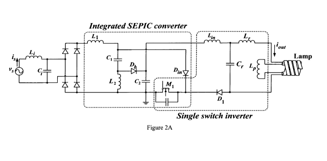
A single switch electronic ballast according to one embodiment is shown in the
schematic diagram of Figure 2A. This embodiment is based on a cascade
combination of
a single ended primary inductor converter (SEPIC) for the PFC stage and a
single switch
current fed inverter. Other types of converters may of course be used, such
as, for
example, boost (see Figure 2E) or flyback (see Figure 2F). Such alternative
converters
may reduce the number of circuit elements and complexity of the electronic
ballast. Other
converters, such as buck-boost, may also be used, however, use of a converter
that
employs more than one switch would increase the complexity, cost, and size of
the
electronic ballast circuit.
-10-
CA 02727529 2010-12-09
WO 2009/149556 PCT/CA2009/000824
The SEPIC may be used for the PFC stage in this embodiment because: (1) it
does
not require a large size high-voltage DC link capacitor (in contrast with
designs using a
boost PFC); (2) unlike a discontinuous conduction mode (DCM) operating boost
converter, the SEPIC converter DC-link capacitor is not subjected to high
voltage stress in
order to achieve a high power factor [11]; (3) the output DC link voltage
polarity is not
inverted (in contrast with designs employing a buck-boost converter), which
allows
simpler circuit configuration and input EMI filter designs [12]. Further,
relative to prior
designs based on boost and buck-boost converters, the SEPIC does not include
an inductor
in the ground path (as can be seen in Figure 2A), which reduces noise and
allows for fewer
components in the EMI filter, which allows for smaller size of the ballast
circuit. When
the SEPIC operates in DCM with a fixed switching frequency, the peak of the
DCM
inductor current also follows the rectified sinusoidal envelope and a close-to
unity power
factor is achieved at the input. As a result, a SEPIC converter has all the
advantages of
boost and buck-boost converters, and only requires an extra inductor and
capacitor.
Referring to Figure 2A, the line voltage is connected to optional an EMI
filter
including Li and Ci, and then to a rectifier circuit. As an alternative to the
EMI filter of
Figure 2A, a common mode EMI filter such as that shown in Figures 2E or 2F may
also be
used. That is, the EMI filters of Figure 2A and of Figures 2E and 2F may be
interchanged.
The output of the rectifier feeds the SEPIC circuit. The SEPIC includes
inductors L1, L2,
capacitors C1, C2, diodes Db, Din, and a switch Ml. The switch is shown with
its intrinsic
drain-source capacitor. In some embodiments the input EMI filter Li, Ci may be
eliminated by properly selecting appropriate (e.g., smaller) values of L2 and
Cl. This may
simplify the design of the entire circuit.
The current fed inverter includes inductors Lin, Lr, LP, capacitor Cr, diode
D1, and
the switch MI. Capacitor Cr and inductors Lin, Lr form a C-L-L resonant
circuit. An
alternative arrangement of the inverter is shown in Figure 2D, wherein
inductors L, and Lp
are arranged as a centre-tapped inductor or an autotransformer. It is noted
that the
arrangement of Figure 2D may be used with the electronic ballast circuits of
Figures 2A,
2E, and 2F. The switch MM is operated by providing a suitable signal to the
control or gate
terminal. Thus, as can be seen, the switch is shared between the SEPIC circuit
and the
inverter circuit.
The switch may be a MOSFET or other suitable switching device, such as, for
example, IGBT (insulated gate bipolar transistor), or MCT (MOS controlled
thyristor). A
-11-
CA 02727529 2010-12-09
WO 2009/149556 PCT/CA2009/000824
bipolar transistor may also be used, with appropriate driver circuit.
Selection of a suitable
switching device may depend on factors such as power handling capability of
the switch,
as will be apparent to one of ordinary skill in the art.
Operation of the switch may be achieved many different ways, and includes
setting
the duty ratio of the switch. For example, in one embodiment the switch may be
operated
at a fixed duty ratio by providing a fixed pulse signal to the gate terminal.
Such an
embodiment is shown in Figure 2B. This embodiment may provide stable operation
of the
ballast circuit at normal line voltages and also during brownout conditions
with proper
selection of the duty ratio. The duty ratio may be selected for, e.g., worst-
case brownout
conditions, characterized by, e.g., a selected percentage drop in the line
voltage. The duty
ratio may be calculated using equations (15) and (16) below, solving for d.
An example of how the switch may be operated with a variable duty ratio is
shown
in the embodiment of Figure 2C. This embodiment tracks the line voltage and
provides a
variable duty ratio signal to the switch so as to compensate for fluctuations
in the line
voltage, including brownout. This embodiment uses the DC voltage from the
ballast
circuit and a reference voltage to generate an error signal which determines
the duty ratio.
This embodiment may compensate for a line low voltage and avoid glow-discharge
mode
operation. In a further embodiment the reference voltage may be adjusted to
compensate
for brownout and/or to avoid glow-discharge mode operation. A variable
reference
voltage may be used for this purpose.
Description of Operation
Operation of the embodiment of Figure 2A is described below with reference to
Figure 3 which shows the operating stages (intervals 1 to 4), with key
waveforms shown in
Figure 4. Figure 5 shows operating waveforms at the PFC side to achieve high
power
factor in DCM.
Let the input line voltage be: ve(t) = Vpsin(2irfLt) with Vp = peak line
voltage and fL
= line frequency; the average current (is g(t)) drawn from the line is given
in (1), where
Leq = (L1L2)1(L1+L2) [12], TS = switching period and d= duty ratio. It is
observed from (1)
that is,qõg(t) is pure sinusoidal and is in phase with v,5(t). Hence, a very
high power factor is
achieved at the input. The input average power equation is derived from (1) as
given in
(2).
-12-
CA 02727529 2010-12-09
WO 2009/149556 PCT/CA2009/000824
[interval 11: M1 is on, iL rises linearly, inn begins to increase slowly due
to the presence
of L;,, so that close to zero-current switching is provided at the turn-on of
the MOSFET.
The total current flowing through the switch is ids.
[interval 21: M1 is off, iL decreases linearly. Current im flows through Coss
and decreases
until it drops to zero.
[interval 3]: iL continues to decrease linearly until it drops to zero, then
iL enters the
discontinuous conduction period.
[interval 4]: all the diodes are off and the resonant circuit continues to
deliver the
required energy to the output.
T V d 2 T
is,avg (t) = T Ji(tid(a)t) = 2L s sin(2~fLt) (1)
TS 0 e9
1 T V2d2T
Pavg =- Jvs(t)isavg(t)d(0t) = s (2)
4L9
Analysis of Resonant Inverter
The corner frequency (,t) and the quality factor equation of the C-L-L
resonant
inverter are determined by (3) and (4) respectively. As the voltage generated
across Cr is a
close-to sinusoidal waveform, proper lamp current balancing is ensured at the
output of the
inverter circuit. If a high enough quality factor (Q) is chosen in the
resonant circuit, then
close-to-sinusoidal waveforms can be achieved at the output and fundamental
approximation can be used in the linear analysis of the resonant circuit.
During lamp
ignition, the lamp resistance (Rramp) is infinite and the resonant circuit
becomes a parallel
L-C circuit. The output voltage of the lamp during this phase is given in (5).
By solving
(5), the corresponding ignition frequency may be obtained as given in (6),
where LT =
L,+Lp and I,,, is the amplitude of it,,.
After the lamp is ignited, the gas within the lamp becomes ionized and the
lamp
resistance decreases to a few hundred ohms. The resonant circuit now becomes a
C-L-L
resonant tank with a finite value of lamp resistance. The output lamp current
is then
calculated using the current gain relationship as shown in (7), where im I is
the fundamental
component of i,,,, k = LpILr and cos is the angular switching frequency.
1 (3)
27r T, _C1
-13-
CA 02727529 2010-12-09
WO 2009/149556 PCT/CA2009/000824
Q- rLr
R (4)
lamp
Vout \~~/ _ O)LP
lin,l (JCo) 1 - CO2LTCr IL2 )
+4V LTC' -L
I in 12 v
{' = 1 in `in (6)
J 2'r 2VxõLTC
(7)
iin,l u co) )212 2
w~ + QJ\l+k ~o Q~k ws
Component Stress Analysis
The active components in a single stage or single switch converter may be
subjected to high voltage or current stress when compared to a conventional
two stage
converter to achieve the same power level. Here, the voltage and current
stress across the
switch of the embodiment of Figure 2A are investigated.
As mentioned above, when the MOSFET conducts, the current components include
iL, icl, and ii,. Hence, the maximum current stress occurs at the end of the
conduction time
of the switch, which is given in (8), where iL,pk is the peak current of
inductor L1, iCl,pk is
the peak current of inductor L2, and iin,pk is the peak of the inverter input
current. Since the
voltage across Cl is equal to the rectified line voltage, iCl,pk and iL,pk can
be combined and
the corresponding equivalent inductance is represented by Leq. In (8), vcr(t)
represents the
voltage across capacitor Cr, which is the sum of the voltage across inductor
Lr and the
lamp voltage vo(t); Vdc is the DC link voltage across C2 and Vrect is the
rectified line
voltage. The voltage gain relationship between Vdc and Vrect is given in (9).
Assuming that
a close-to-sinusoidal waveform is achieved at the output, i.e., vo(t) =
Vocos(cost), vcr(t) will
also be a close-to-sinusoidal waveform with a phase angle of cp. The final
expression in
(8) is expressed in terms of vo, Vdc, and Vpk, which are all known quantities
so that the
maximum current stress can be calculated. The peak current flowing through D1,
Din, and
Db are also given in (10), (11), and (12) accordingly.
The rms voltage stress across the MOSFET when the MOSFET is off is given in
(13). It is obtained by using Kirchhoffs Voltage Law, where vL,in(t) is the
voltage across
-14-
CA 02727529 2010-12-09
WO 2009/149556 PCT/CA2009/000824
inductor L,n. Since the current flowing through L,,, is almost equal to zero
when the
MOSFET is off, vL,,n(t) is almost equal to zero as well during the switch off
period. Using
v,t(t) derived earlier in (8) and substituting it in (13) gives a good
approximation of the rms
voltage across the switch.
tds,max = iLl pk + lCl pk + tin pk
'' (8)
= TPk dT + VCl dT +t JVdc -ycr(t - (P)a
~, 4 0 Lin
Iv,,(t)dt+ VPk dT +Vdc dT + 1 1+ Lr Lpr vo(t)
I eq S Lin Ln LP 4n` lamp
Vdc d (9)
Vrec, I- d
~
"
iD, pk = Vdc dT + 1 1 + L" f va (t)dt + va (t) (10)
Lin Lin LP 0 LinRlamp
( )
lD Pk - VPk Leg dT 1 1
1Dõpk = 1D_pk (12)
T, llll
V ds,rms = 7. f( \Vdc - V L,in (t) - vcr (t //2 dt
, 0
T
= 1 f Vdc 1_Lr dvo (t) - 1 + 2
L" va (t) dt (13)
TS Riamp dt L p
Dimmer Function
A standard, commercially available dimmer (e.g., a triac dimmer) as used with
an
incandescent lamp controls the lamp output power by adjusting the conduction
time of the
AC input line voltage. A leading edge dimmer (e.g., a triac or thyristor
dimmer) is an
example of a standard dimmer that chops off the early or leading edge of each
half of the
AC sine wave. Conduction of the device is controlled by a trigger or firing
pulse, and the
later the device is fired and starts to conduct, the less power is delivered
to the lamp. A
trailing edge dimmer (e.g., a transistor dimmer) is an example of a standard
dimmer that
chops off the late or lagging edge of each half of the AC sine wave. Less
power is
delivered to the lamp as more of the trailing edge is chopped.
-15-
CA 02727529 2010-12-09
WO 2009/149556 PCT/CA2009/000824
Thus, with standard dimmers, the shorter the conduction time, the less power
will
be delivered to the output. Hence, the power factor will decrease as the
conduction time
of the dimmer decreases. The poor power factor obtained from a typical CFL at
its full
lamp power implies that such dimmers, when placed between the input and the
CFL, will
result in very poor power factor with extremely high current spike at the
input during
dimming. As a result, such a dimmer should not be used with a currently
available CFL
not only because of the poor power factor, but also because the high current
spike may
exceed the current rating of the circuit components and destroy the electronic
ballast.
Proper dimming performance of a fluorescent lamp may require power factor
correction at all dimming levels. Commercially-available consumer grade
electronic
ballasts, such as those found in CFLs, may not include a PFC circuit, or may
include a
PFC circuit with poor performance. Hence, a commercial CFL produces a poor
power
factor at the AC main input. For example, when a standard phase-cut (triac)
dimmer is
used with a CFL, the dimming range of the lamp is very limited. When the lamp
is
dimmed, flickering is observed at the light output and in some cases, no light
is produced
at low dimming level. Under conditions where the line voltage drops suddenly
(i.e.,
brownout), the lamp cannot sustain its normal operation.
Another aspect of the invention relates to a dimmer controller circuit for an
electronic ballast for a fluorescent lamp. The dimmer controller circuit
maintains a high
power factor throughout the dimming range, and may compensate for brownout
conditions as well as avoid glow-discharge mode operation of the fluorescent
lamp.
An embodiment of a dimmer controller circuit, which includes a duty ratio
controller and a gain multiplier, is shown in Figure 9A. Referring to Figure
9A, a
conventional triac dimmer (TD) is connected to the input of the duty ratio
controller of
the dimmer controller. The output lamp power may be controlled by adjusting
the pulse
width of the switch Mi. The AC line voltage is rectified (Vrect), scaled down
(not shown
in Figure 9A or 9B), and compared with a DC signal in the comparator U 1. At
the output
of the comparator, a pulse is generated when the DC signal is higher than
Vrect= When a
firing angle is applied at to, the rectified voltage is chopped and the
corresponding pulse
width at the output of U1 is increased. This pulse width shows how much firing
angle has
been applied to the triac. The circuit multiplies this pulse width information
by a gain
factor and then subtracts this signal from the reference voltage. The end
result is that a
small firing angle can control a large amount of lamp power so that high power
factor is
always maintained at the input even during dimming.
-16-
CA 02727529 2010-12-09
WO 2009/149556 PCT/CA2009/000824
A dimmer controller circuit according to another embodiment is shown in Figure
12A as used with a trailing edge dimmer. This embodiment, as with all
embodiments,
may of course also be used with a leading edge dimmer. The embodiments
described
herein may also be used with a resistive dimmer. This embodiment allows a
fluorescent
lamp to be dimmed smoothly, and the dimmed light output can be maintained
during
brownout conditions and when the lamp is switched off and on again. This
embodiment
also avoids glow-discharge mode operation of the fluorescent lamp. As shown in
Figure
12A, this embodiment includes a gain adjuster that provides a proper signal to
be
subtracted from a reference signal during dimming. This embodiment also
includes duty
ratio control and a non-linear function (e.g., a multiplier) to accommodate
for the drop in
voltage during dimming. When the main power is switched off and then on again
during
dimming, the multiplier provides a high duty ratio signal to sustain the arc
across the
lamp.
The dimmer controller may be implemented as a discrete circuit design, using
discrete elements and commercially-available semiconductors, or it may be
implemented
as a single integrated circuit in the form of an analog ASIC, or it may be
implemented as
firmware implanted in a digital controller. Analog implementations and digital
implementations may be equivalent functionally, but offer different overall
costs to
implement.
A dimmer controller circuit as described herein may be used with a standard
dimmer, such as a triac or thyristor dimmer (i.e., a leading edge dimmer) that
is typically
used with an incandescent. Other dimmers as known in the art, such as
transistor
dimmers (i.e., trailing edge dimmers) may also be used. The dimmer controller
circuit
may be provided alone, for use with an electronic ballast, or together with an
electronic
ballast. In the latter case, the dimmer controller circuit and the electronic
ballast circuit
may be combined, e.g., substantially or completely in one circuit. Such an
embodiment
may be produced in a compact size, suitable for use with a CFL. For example,
the
dimmer controller of the embodiment of Figure 12A may be combined with the
electronic
ballast circuit of Figure 2A, as shown in Figure 12B. Alternatively, the
embodiment of
Figure 12A may be combined with the electronic ballast circuit of Figure 2E or
2F.
A dimmer controller as described herein may be used with electronic ballasts
whose operation is based on duty cycle variation and with electronic ballasts
whose
operation is based on frequency variation. The embodiments shown in Figures 9A
and
12A, configured to control a single switch, allow control of the duty ratio
substantially
-17-
CA 02727529 2010-12-09
WO 2009/149556 PCT/CA2009/000824
from 0 to 100% (i.e., maximum dynamic range of the switch). However, it will
be
appreciated that a dimmer controller as described herein is not limited to use
with single-
switch electronic ballast such as that shown in Figure 2A, 2E, or 2F. The
dimmer
controller may be configured for use with electronic ballasts having two or
more switches
by providing drive signals with appropriate duty ratios to each switch. For
example, the
embodiment of Figure 12C includes dead-time control and phase shift functions
to drive
both switches of a two-switch electronic ballast with appropriate duty cycles.
Such a
dimmer controller may be provided alone, or in combination with an electronic
ballast
having two or more switches, as shown in Figure 12C. Such a dimmer controller
for two
switches allows for variation of the duty ratio substantially from 0 to 50%
for each
switch.
Another aspect of the invention relates to a combination comprising an
electronic
ballast and a dimmer controller, for use with a fluorescent lamp. The
electronic ballast
with dimmer controller has a high power factor throughout the dimming range.
The
dimmer controller may use a standard, commercially available dimmer, such as a
triac
dimmer, a transistor dimmer, or a resistive dimmer typically used for an
incandescent
lamp. The dimmer controller may include a duty ratio controller and a gain
multiplier.
One embodiment of the combination includes a high power factor electronic
ballast circuit, such as, for example, the embodiment shown in Figure 2A, 2E,
or 2F, and
a dimmer controller, such as the embodiment shown in Figure 9B or Figure 12A.
The
dimmer controller may control a wide range of fluorescent lamp light output by
adjusting
only a narrow range of firing angle. As a result, a change of only several
firing angle
degrees results in significant drop in the light output. The overall system
features high
power factor performance throughout the entire dimming range with the
electronic ballast
power circuit being extremely compact.
An embodiment of a combination comprising an electronic ballast and a dimmer
controller is shown in Figure 12B. This embodiment includes a shared switch
electronic
ballast such as that shown in Figure 2A. According to this embodiment, the
duty ratio of
the switch MI in the power circuit is controlled. By controlling the duty
ratio of the
switch, the lamp output power may be adjusted. Vrec1, a feed-forward
parameter, carries
information of the firing angle applied to the lamp dimmer to the dimmer
controller.
During normal dimming operation, when part of the sinusoidal line voltage is
chopped,
the power transferred to the output will naturally decrease. Hence, the duty
ratio of the
-18-
CA 02727529 2010-12-09
WO 2009/149556 PCT/CA2009/000824
switch does not drop below a selected level so as to avoid glow-discharge mode
of the
lamp. The gain (K) signal, Vol*K, is subtracted from an initial reference,
VYefl, to force
the duty ratio to decrease slightly during dimming. In other words, VYef =
Vrejr - Vo1K
during dimming. The multiplier allows a slight increase in the duty ratio to
provide a
high enough voltage at the output to sustain the lamp arc during dimming. As a
result,
the output signal of the multiplier is relatively small compared to Vrej so
that the presence
of the multiplier inside the controller does not affect the normal operation
of the ballast
circuit.
It will be appreciated that a dimmer controller as described herein may be
used
with electronic ballast circuits other than an electronic ballast circuit as
described herein.
However, modification of the dimmer controller may be required; such as, for
example,
adding controller/driver stages to drive any additional switches in the
ballast circuit. For
example, the combination may include an electronic ballast having two or more
switches,
and a dimmer controller as described herein, such as the embodiment shown in
Figure
12C. An example of such an electronic ballast is a two switch power circuit
using a
conventional half bridge inverter, as shown in Figure 12D. Another aspect of
the
invention relates to a fluorescent lamp including an electronic ballast as
described herein.
In one embodiment, the fluorescent lamp may include a combination of an
electronic
ballast circuit and a dimmer controller circuit as described herein. In
another
embodiment, the fluorescent lamp may be a compact fluorescent lamp (CFL).
Another aspect of the invention relates to a socket for a fluorescent lamp
including
at least one of an electronic ballast circuit and a dimmer controller circuit.
The electronic
ballast circuit may be as described herein. The dimmer controller circuit may
be as
described herein. In one embodiment, the fluorescent lamp may be a CFL.
It will be appreciated that in applications where lamp dimming is not
required, a
dimmer controller as described herein may be used without a dimmer to control
an
electronic ballast. Here, the controller may be referred to as a ballast
controller or simply
as a controller. Such an embodiment is shown in Figure 12E. This arrangement
provides
operation of the lamp at full brightness and with a very high power factor,
and in
particular, maintains such operation of the lamp when the line voltage drops
below
normal levels (e.g., during brownout). Such a controller may be used in all
embodiments
and aspects described herein, in applications were a dimming function is not
required.
Another aspect of the invention provides a dimmer for use with an electronic
ballast and a dimmer controller circuit as described herein to dim a
fluorescent lamp, such
-19-
CA 02727529 2010-12-09
WO 2009/149556 PCT/CA2009/000824
as a CFL.Conventional incandescent lamp phase-cut dimmers (leading edge or
trailing
edge) control the light output by adjusting the conduction angle of the input
sinusoidal
line voltage. One major drawback with such dimmers is that the conduction
angle of the
line voltage and the line current decrease when the lamp is dimmed. This means
the
power factor decreases to a low value at very low dimming level. To solve this
problem
and to maintain simple wiring between the dimmer and the rest of the system, a
dimmer
as described herein does not control the light output by controlling the
conduction angle
of the line voltage. Rather, it controls the light output by injecting a high
frequency (HF)
signal using a voltage-controlled oscillator (VCO). Figure 17A is a block
diagram of an
embodiment of the dimmer, interfaced with ballast and dimmer controller
circuits as
described herein. The frequency range of the high frequency signal should be
sufficiently
different from the frequency at which components of the electronic ballast
circuit operate,
to avoid interference. For example, if the electronic ballast operates in the
kHz range, the
high frequency signal should be in the MHz range. Specific operating
frequencies are a
matter of design choice and can be easily determined by one of ordinary skill
in the art.
As shown in Figure 17A, the input of the VCO, which is a DC voltage signal, is
the user control interface. The controller circuit includes a frequency to
voltage
conversion block before the control logic block, which includes a PWM
comparator.
This block converts the HF signal into a DC voltage (V,,,,), The higher the
frequency of
the HF signal, the higher the magnitude of VV0,,. This conversion may be done
by, for
example, detecting time between two zero-crossing points of the HF signal and
then
converting the value into an appropriate corresponding voltage level. In this
embodiment,
a higher frequency implies that there is less time required between two zero-
crossing
points; hence, the output DC voltage level increases inversely and
proportionally.
Commercially-available ICs such as AD650 (Analog Devices) and LM2917 (National
Semiconductor) may be employed for this task. V,oõ is then fed to the PWM
block to
adjust the duty ratio of the switch of the ballast power circuit, which
determines the light
output. In the embodiment of Figure 17A, the HF and low frequency 60Hz signals
need
to be separated, and an L-C circuit (Lfl and Cfl) may be used for this
purpose.
As noted above, the input of the VCO, which is a variable DC voltage signal,
is
the user control interface. This may be implemented many different ways, as
known in
the art. For example, the DC voltage signal may be controlled using a simple
potentiometer, or by a computer/microprocessor and/or additional circuitry for
ramping
the DC voltage signal, which may be carried out manually or automatically in
response to
-20-
CA 02727529 2010-12-09
WO 2009/149556 PCT/CA2009/000824
one or more stimuli. As to the latter, sensors, such as for voice recognition
and/or for
sensing one or more of, but not limited to, light (e.g., visible, infra-red,
UV), sound (e.g.,
voice), mechanical stimuli (e.g., vibration, pressure), temperature,
humidity/moisture, air
movement/wind, or one or more chemicals, may be used in conjunction with such
computer/microprocessor and/or additional circuitry to control the DC voltage
signal.
As shown in Figure 17A, the output high frequency signal may be fed to the
controller circuit over the same power lines that supply AC power to the
electronic ballast
circuit. Alternatively, the output high frequency signal may be fed to the
controller over
separate conductors, or it may be transmitted to the controller using any
other suitable
technique, such as wirelessly, using, for example, radio waves or infrared
light, as known
in the art.
Figure 17B shows a detailed implementation of an embodiment of the dimmer.
This embodiment includes a diode D;, resistor RS and capacitor C; which
convert the AC
line voltage to a DC signal. Resistor Rvar is a variable voltage divider so
that the DC
voltage at the input of the VCO can be adjusted by the user.
A dimmer as described herein maintains very high power factor (close to unity)
at
the AC line input side throughout the entire dimming range, with low cost.
Embodiments of the invention are further described in the following non-
limiting
working examples.
Working Examples
1. Electronic Ballast Circuit
Performance of an electronic ballast circuit based on the embodiment of Figure
2A was verified through simulation and an experimental prototype. A Sylvania
Dulux
T/E 4-pin 26 W CFL with Iout= 0.32 AõS was chosen as the testing load for the
prototype
with a line voltage of 110 V,,,,, 60 Hz. The switching frequency was 70 kHz
and the
quality factor was 2. The circuit parameters were calculated using the
following steps:
(1): Ria,,,p was first calculated using Ioõt and Poõr as shown in (14). Then
the values of Lr, Cr
and Lp were obtained using (3), (4) and (5) respectively.
)
PP, _ 26W " 250 (14)
Rlamp I2 (o.32 2500 l
.14l
-21-
CA 02727529 2010-12-09
WO 2009/149556 PCT/CA2009/000824
QRmmp - 2(25052)
L, -
2nf, 27r(70kHz) 1. 1mH
_
1 _ 1
C' (2~tf)2 L, (27r70kHz)2 (1.1mH) _4 .7nF
Lp was selected to be higher than L, so that sufficient high voltage would be
guaranteed at
the output during lamp ignition. In this example, L. was selected to be 1.8
mH.
(2): Calculations ofLi, L2, C2
The SEPIC inductors (LI and L2) were calculated by (2) as follows, with Vpk =
155
V; d = 0.4; T, = 1/70 kHz; and 7 = 90%:
L ,q r/V ;rd2Te _ 09(155V)2(0.4)2(1/70kHz) , 0.55mH
e9 4Povg 4(26W)
Since L1 was chosen to be equal to L2, L1 and L2 were determined from Leq and
were 1.2 mH. The output capacitor C2 was obtained by first calculating the
mean input
resistance of the inverter circuit. This was obtained by equating the input
power of the
SEPIC circuit and the output power of the SEPIC circuit as given in (15)
assuming 11=
90%. From (15), R, was calculated to be 2110 0. Vd, was then calculated from
(9) with d
= 0.4 and Vpk = 155 V. C2 was calculated using (16) by allowing a 2% ripple in
Vd,
2 2 2
vk d T, = Vdc (15)
4Leq IR.
C = VdCdT _ (155vXo.4X1/7okHz) 21 (16)
2 AVd,R; 3V(211 rK )
(3): Selection of MOSFET and diodes
The selection of the MOSFET was determined by both (8) and (13). From (8), the
approximated maximum current stress was calculated with Vpk = 155 V, d = 0.4,
T, = 1/70
kHz, Lin = 1.1 mH.
'Amm=(155VJ.4((1/ 0kHz)+(10300.4('/7c*H. +0.3A=1.95A
The rms switch voltage was determined to be 460 V using (13). To meet these
two
requirements, the MOSFET SPA06N6OC3 (Infineon, Milpitas, California, USA) was
chosen for this design. For the diodes, ultra-fast recovery diodes are
required for diodes
Db, Din, and D1. As illustrated in (10)-(12), the maximum current flowing
through Db and
Din are equal to the peak of the DCM inductor current; whereas the maximum
current
-22-
CA 02727529 2010-12-09
WO 2009/149556 PCT/CA2009/000824
going through D1 is equal to the peak of im. Hence, MUR1560 was selected for
these
diodes.
Simulation and Experimental Results
The circuit simulation was verified in SIMETRIX 5.0 circuit simulation
software
(Catena, Thatcham, Berkshire, UK). Figure 6A shows the simulated line current,
where a
power factor of 0.995 was achieved. Figure 6B shows the simulated output
current iout
and PFC inductor current iL. Figure 6C shows the low frequency component of
the
simulated DCM input inductor current.
Figure 7 is an electrical diagram of the experimental prototype. Figure 8A-E
shows the experimental waveforms of the circuit of Figure 7. The lamp current
and
voltage are shown in Figure 8A, where a crest factor of 1.48 was measured. The
measured current waveforms iout and iL are shown in Figure 8B. The measured
line
current is shown in Figure 8C. A power factor of 0.995 and a THD of less than
10% were
achieved according to the harmonic spectrum of is shown in Figure 8D. Figure
8E shows
the switch current (ids) and switch voltage (vds) waveforms. The peak current
flowing
through the switch was about 1.98 A. All the measured waveforms have good
agreement
with the theoretical waveforms and simulation results. The overall efficiency
was
measured to be 91.8% at 110 V.
2. Electronic Ballast Circuit with Dimmer Controller
(i) An electronic ballast circuit with dimmer controller based on the
embodiment
shown in Figure 9B was built (see Figure 10) and tested. A Sylvania Dulux T/E
4-pin
26 W CFL with Iou,= 0.32 Ar,,,, was chosen as the testing load for the
prototype circuit
with a line voltage of 110 V ms 60 Hz. The switching frequency was 70 kHz and
the
quality factor was 2. Figure 11 A shows the line current under full lamp
power, where a
power factor of 0.96 was achieved. Figure 11 B shows the line current with a
firing angle
of 35 applied to the triac dimmer, where the power factor was 0.86. At this
level of
firing angle, the lamp current was substantially reduced to 0.1 A at a dimming
level of
10% of the lamp rated power.
(ii) An electronic ballast circuit with dimmer controller based on the
embodiments
shown in Figures 2A and 12A was built and tested.
-23-
CA 02727529 2010-12-09
WO 2009/149556 PCT/CA2009/000824
Performance was verified through use of the combination electronic ballast
circuit
with dimmer controller with a four pin 13W CFL. A 15W General Electric (GE)
dimmable CFL (FLE15HT3/2/SW) was used as a reference product for performance
comparison. The dimmers used in the experimental setup were standard phase-cut
leading edge (triac) and trailing edge (transistor) dimmers, both from Leviton
Mfg. of
Canada Ltd. Figure 13A shows the line current of the 15W GE lamp under full
power,
where the power factor was 0.85. Figure 13B shows the line current of the 15W
GE lamp
with the smallest firing angle (i.e., fully dimmed) using the standard
incandescent
dimmer. The power factor at this power level was 0.62. The high peak current
waveform
results in a poor power factor as the conduction angle of the line current
decreases during
dimming. For this reason, the dimming range is very limited in the commercial
dimmable
CFL. Further, when the line voltage drops, this lamp is unable to sustain the
arc across
the lamp and the light will turn off in this situation.
Results for the electronic ballast circuit with dimmer controller are shown in
Figures
14A-D. Figure 14A shows the line current at full lamp power for the trailing
edge
dimmer, where the power factor was 0.97. Figure 14B shows the line current at
the
lowest dimming level for the trailing edge dimmer, where the power factor was
0.84.
When fully dimmed, no lamp flickering was observed and glow-discharge mode
operation was avoided. Figure 14C shows the line current at full lamp power
for the
leading edge dimmer, where the power factor was 0.98. Figure 14D shows the
line
current at a partial dimming level for the leading edge dimmer, where the
power factor
was 0.86.
Figure 15 summarizes and compares the power factor achieved from the
electronic
ballast circuit with dimmer controller, using the trailing edge dimmer and the
13 W CFL,
and the GE 15 W dimmable CFL. It is observed that there is a significant
improvement
of more than 20% in power factor of the embodiment of Figure 12, relative to
the
commercially-available dimmable CFL. The dimming range of the CFL is also much
wider with the embodiment of Figure 12, relative to the commercially-available
dimmable CFL. The efficiency plot shown in Figure 16 shows that an efficiency
of close
to 0.9 was achieved at the rated power in the embodiment of Figure 12,
relative to about
0.81 in the commercially-available dimmable CFL.
-24-
CA 02727529 2010-12-09
WO 2009/149556 PCT/CA2009/000824
Equivalents
Those skilled in the art will recognize, or be able to ascertain, equivalents
to the
embodiments described herein. Such equivalents are considered to be
encompassed by
the invention and are covered by the appended claims.
-25-
CA 02727529 2010-12-09
WO 2009/149556 PCT/CA2009/000824
References
[1l National Resources Canada, "Commercial and Institutional Retrofits -
Technical
Information - Fluorescent Lamp And Ballast Options" 2002.
[21 International standard IEC 1000-3-2 Class C. led, March 1995.
[3] T.-F. Wu and T.-H. Yu.; "A unified approach to developing single stage
power
converters", IEEE Trans. on Aerospace and Electronic Systems, vol. 34, no. 1,
1998,
pp. 211-223.
[4] A.J. Calleja, J.M. Alonso, J. Ribas, E. Lopez, J. Cardesin, J. Garcia and
M. Rico-
Secades, "Electronic ballast based on single-stage high-power-factor
topologies: a
comparative study", in Proceedings of the 2002 IEEE Industrial Electronics
Society
Conf, pp.1196 - 1201.
[51 Alonso, J.M., Calleja, A.J.; Ribas, J., Corominas, E.L., Rico-Secades, M.,
"Analysis
and design of a novel single-stage high-power-factor electronic ballast based
on
integrated buck half-bridge resonant inverter", IEEE Trans. on Power
Electronics,
vol. 19, no. 2, March 2004, pp. 550 - 559.
[6] Chiu, H.-J., Lin, L.-W., Wang, C.-M., "Single-stage dimmable electronic
ballast with
high power factor and low EMI", in Proceedings of the 2005 Electric Power
Applications Conference, pp. 89 - 95.
[7] DeMorais, A.S., Farias, V.J.; deFreitas. L.C., Coelho, E.A.A., Vieira,
J.B., Jr., "A
high power factor ballast using a single switch with both power stages
integrated",
IEEE Trans. on Power Electronics, vol. 21, no. 2, March 2006, pp. 524 - 531.
[81 Weihong Qiu; Moussaoui, Z.; Wenkai Wu; Batarseh, I., "Single-switch zero-
voltage-
switching high power factor electronic ballast", in Proceedings of the IEEE
2002
Power Electronics Specialists Conference, pp. 773 - 778.
[9] Ponce, R. Vazquez and J. Arau, "High power factor electronic ballast for
compact
fluorescent lamps based in a class E amplifier with LCC resonant tank", in
Proceedings of the 1999 IEEE Applied Power Electronics Conference, pp. 486-
492.
[1o] Cheng, H.L.; Moo, C.S.; Yen, H.C.; Lin, T.F.; Huang, S.H.; "Single-switch
high-
power-factor electronic ballast for compact fluorescent lamps", in Proceedings
of the
2001 IEEE International Conference on Power Electronics and Drive Systems, pp.
764-769.
-26-
CA 02727529 2010-12-09
WO 2009/149556 PCT/CA2009/000824
~1 iI Liu, K.-H.; Lin, Y.-L.; "Current waveform distortion in power factor
correction
circuits employing discontinuous-mode boost converters", in Proceedings of the
1989
IEEE Power Electronics Specialists Conference, pp. 825 - 829.
[12] Simonetti, D.S.L.; Sebastian, J.; Uceda, J.; "The discontinuous
conduction mode
Sepic and Cuk power factor preregulators: analysis and design", IEEE Trans on
Industrial Electronics, vol. 44, no. 5, Oct. 1997, pp. 630 - 637.
[13] Lam, J.; Jain, P.; "A low cost single-stage electronic ballast with unity
power factor
using a novel single switch current fed resonant inverter topology", in
Proceedings of
the 2007 IEEE Power Electronics Specialists Conference, 17-21 June 2007, pp.
3106
-3111.
-27-