Note: Descriptions are shown in the official language in which they were submitted.
CA 02727912 2010-12-13
WO 2009/153764 PCT/IB2009/052658
1
ELECTRO-OPTICAL DEVICES USING DYNAMIC RECONFIGURATION OF
EFFECTIVE ELECTRODE STRUCTURES
FIELD OF THE INVENTION
This invention relates to the field of electrically tunable optical devices,
particularly
those using liquid crystal.
BACKGROUND OF THE INVENTION
Tunable liquid crystal (LC) optical devices, such as lenses, beam steering
devices and
shutters are known in the art. While some tunable LC lenses operate with a
uniform
electric or magnetic control field, most use a spatially modulated field. In
the case of
electric fields, there are a few prior art techniques used to spatially
modulate the
electric field. Spatially inhomogenous dielectric layers have been used to
attenuate the
electric field to have a desired spatial profile. Electrodes have been
spherically shaped
to provide a desired spatial profile to the electric field. Another approach
to spatially
modulating the electric field is to use a planar electrode whose impedance
properties
are such that the voltage drop over the electrode as AC drive current is fed
to the
electrode leads to a spatially modulated electric field.
As shown in Figure 1, one type of conventional LC cell is built by sandwiching
the
liquid crystal 102 between two substrates 104,106, each of which is first
coated by a
transparent electrode 108, 110, which may be a layer of material such as
indium tin
oxide (ITO), and then coated by polymer layers 112 (typically polyimide) which
are
rubbed in a predetermined direction to align LC molecules in a ground state,
namely in
the absence of the controlling electric field. The application of voltage to
two ITOs
creates a uniform electric field and correspondingly uniform LC reorientation
(and
correspondingly uniform refractive index distribution). In such a device, the
index of
refraction is different in a direction lengthwise with respect to the
molecules than
transverse to the molecules.
Figures 2 illustrates a prior art LC cell configuration, in which a hole
patterned
electrode ring 204 of low resistivity surrounding a disk-shaped zone 205 of
high
resistivity material is used to generate an electric field gradient thanks to
its strong
"resonant" attenuation. This geometry has the advantages of being very thin
(which is
a key requirement, e.g., in cell phone applications) and of using only two
electrodes
(and thus one voltage for control). Unfortunately, it is difficult to produce
the required
thickness of high resistivity material with high optical transparency, as well
as an LC
CA 02727912 2010-12-13
WO 2009/153764 PCT/1B2009/052658
2
cell with good uniformity, and the manufacturing process typically has a low
yield.
Different lenses will have slightly different electrode resistances and this,
coupled with
the fact that modal control is also very dependent on the precise cell
thickness, means
that each individual lens needs to be calibrated separately. Also, the minimum
diameter of a modal lens is limited to about 2mm - below this size the
required
resistivity of the ITO layer exceeds some 1 OMQ/sq. Finally, such (so called
"modal
control") lenses must always be either positive or negative. It is not
possible to switch
between a diverging and converging lens.
Figure 3 illustrates another prior art LC cell configuration with electric
field gradient
generation, using three distinct electrodes 304, 305, 307 (two of them in the
inter-hole
pattern formed on the same plane), two voltages V1 and V2 and an additional
distinct
weakly conductive layer (WCL) 306. The role of the external hole patterned
electrode
304 (with voltage V1 applied thereto) is to create a lens-like electric field
profile, while
the role of the central disk-shaped electrode 305 (with voltage V2 applied
thereto) is to
avoid disclinations and to control the value of the gradient (e.g., to erase
the lens).
The role of the WCL 306 is to soften the profile created by V1 and to allow
the
reduction of the overall thickness of the lens. Unfortunately, the complex
patterning of
the top electrode, the necessity of using two distinct voltages and a separate
WCL are
difficult to manufacture and inhibit the practical use of this approach. For
example, the
use of this approach to build a polarization independent lens would require
the use of
six to seven thick glasses, which is a difficult task.
SUMMARY OF THE INVENTION
In accordance with the present invention, a variable optical device is
provided for
controlling the propagation of light passing therethrough, where the device
makes use
of a frequency dependent material and an electrical signal generator that
generates a
drive signal at a plurality of different frequencies. The device includes a
liquid crystal
(LC) layer through which the light passes, the LC layer controlling the light
propagation. An electrode system is also provided that is connected to the
electrical
signal generator and arranged to generate an electric field that acts on the
LC layer to
alter its optical properties. The electrical signal generator generates a
drive signal at a
plurality of different frequencies and supplies the drive signal to the
electrode system
so as to generate the electric field. The frequency dependent material is
located in the
device so that it interacts with the electric field. This material has a
charge mobility
CA 02727912 2010-12-13
WO 2009/153764 PCT/IB2009/052658
3
that is dependent on a frequency of the drive signal such that a spatial
profile of the
electric field varies as a function of the drive signal frequency to alter the
properties of
the LC layer. "Charge mobility" is used to describe the property of the
frequency
dependent material instead of "conductivity" because the latter can be
understood to
describe the mean free path of electrons. At low frequencies, some frequency
dependent materials that exhibit high charge mobility may actually have lower
conductivity (i.e. a shorter mean free path of electrons) than at higher
frequencies,
however, since the time for the charge to flow within the frequency dependent
material
is longer at low frequencies, this can result in less charge flow. Similarly,
at higher
frequencies, the mean free path of electrons in some materials may be longer,
however, given the shorter time that the electric potential is available in
each positive
or negative cycle, the resulting charge flow may be greatly reduced. Thus
"charge
mobility" is used to refer to the overall ability of charge to flow within the
frequency
dependent material within the constraints of the alternating electric signal
applied.
In some embodiments, the electrode system comprises a fixed conductor
electrode
connected to a body of the frequency dependent material. The electric field
may have
a portion substantially defined by the fixed conductor electrode, and a
portion defined
by the frequency dependent material. The electric field may also be
substantially
defined by the frequency dependent material. The electrode system can have a
fixed
conductor electrode whose electric field is shaped by a body of the frequency
dependent material that is not connected to the fixed conductor electrode.
In some embodiments, the electrode system is made using elements having a
substantially flat layer geometry.
The electrode system may also be essentially optically hidden and thus may not
interfere with the propagation of light through the optical device.
In some embodiments, the electrode system comprises a patterned electrode in
contact with a layer of the frequency dependent material.
In some embodiments, the device is a tunable focus lens. The lens can be
refractive
or diffractive.
In some embodiments, the device includes a variable frequency control signal
circuit
configured to cause the device to control propagation of light as a function
of control
signal frequency.
The use of a frequency dependent material and a drive signal at different
frequencies
allows for a variety of different embodiments of the optical device. Some
examples of
CA 02727912 2010-12-13
WO 2009/153764 PCT/1B2009/052658
4
variations are the number, shape and configuration of electrodes, the number
of
different frequency dependent materials and their positions relative to the
electrodes
and each other, the application of different drive signal frequencies and
voltages and
the use of additional materials in the optical device structure. In one
embodiment, the
drive signal comprises a single frequency signal for which the frequency is
used to
change the optical characteristics of the device. This may be done without any
significant variation in the signal voltage, or it may also include changes in
signal
amplitude. In another embodiment, a plurality of frequencies are mixed
together and
applied simultaneously to create a particular interaction with the frequency
dependent
layer and, correspondingly, to create a desired profile for the electric
field.
A basic concept of the invention is using a frequency dependent material in
conjunction with different drive signal frequencies in order to change an
effective
electrode structure within the optical device. The electrode structure
determines the
profile of the electric field which, in turn, determines the optical
properties of the LC
layer. The frequency dependent material may be selected to exhibit different
charge
mobility at different frequencies such that, at different frequencies, it may
appear as a
conductive or as a non-conductive material. For frequencies at which it
appears as a
conductor, the frequency dependent material may create an effective electrode
structure that is positioned differently than one of the fixed electrodes.
However, for
frequencies at which charge mobility in the frequency dependent material is
relatively
low, it does not appear as a conductor, and the effective electrode structure
is
determined by the actual position of the fixed electrodes. Thus, with proper
positioning of a frequency dependent material, and the selection of different
drive
frequencies, the effective conductor configuration may be altered and the
optical
properties of the LC layer dynamically changed.
In one group of embodiments, a frequency dependent material is used in
conjunction
with a patterned electrode that, in the absence of a different electrode
structure, would
create a spatially non-uniform electric field. Such a structure may be used
for creating
a particular characteristic in the LC layer, such as a lens structure,
resulting from the
non-uniform reorientation of the LC molecules by the electric field. In such
an
embodiment, however, it may also be desirable to create a spatially uniform
electric
field so as to provide an initial common alignment tendency to all of the LC
molecules
(e.g., to avoid disclinations). In this embodiment of the invention, the
frequency
dependent material may be located such that, when a frequency of the drive
signal is
CA 02727912 2010-12-13
WO 2009/153764 PCT/IB2009/052658
selected that provides a high degree of charge mobility (which allows charges
to travel
larger distances) in the frequency dependent material, an effective electrode
structure
is created that causes the spatial profile of the electric field to be
essentially uniform.
For example, the patterned electrode could be a ring electrode, and a space in
the
5 center of the electrode filled with the frequency dependent material. In
such a case,
the application of the drive signal at a first frequency, such as a relatively
high
frequency, for which there is little charge mobility (i.e., relatively small
distances
travelled by charges) in the frequency dependent material, results in no
effective
extension of the electrode surface, and a non-uniform electric field is
generated based
on the ring structure of the electrode. However, changing to a frequency, such
as a
relatively low frequency, at which the frequency dependent material has a
relatively
high amount of charge mobility causes the material to appear as an extension
of the
ring electrode, and the effective electrode structure becomes planar. As such,
the
electric field generated thereby is essentially uniform. In the foregoing
embodiment,
other shapes may be used for the fixed electrode, such as a disk shape, and
the
frequency dependent material may form a layer with the fixed electrode located
near
either the top or bottom of the layer, or surrounding it in the same plane.
In another embodiment of the invention, the variable optical device includes a
central
layer positioned between two LC layers. Each of the liquid crystal layers may
have a
different direction of LC orientation. A pair of electrodes to which the drive
signal is
applied are located, respectively, adjacent to each LC layer, to the side away
from the
central layer. The central layer includes a particular geometric arrangement
of a fixed
electrode, such as a hole patterned electrode, and a frequency dependent
material,
and functions as a gradient control layer by shaping the electric field seen
by each of
the LC layers in a symmetrical way. This electric field shaping is dependent
on the
frequency of the drive signal, which determines the extent of charge mobility
in the
frequency dependent layer. At a frequency corresponding to low charge
mobility, the
gradient control layer shapes the electric field according to the shape of the
fixed
central layer electrode. At a frequency corresponding to high charge mobility,
however, the frequency dependent layer creates an effective electrode surface,
and
the gradient control layer shapes the electric field according to an overall
electrode
geometry resulting from the electrode and the frequency dependent layer
together.
In another embodiment of the invention, the optical device has a plurality of
frequency
dependent materials that have differing amounts of charge mobility at certain
CA 02727912 2010-12-13
WO 2009/153764 PCT/IB2009/052658
6
frequencies. These materials may be arranged together in a particular
geometrical
configuration to create a dynamically adjustable effective electrode shape.
For
example, the two materials may be located in a common layer with one of the
materials having a lens-like shape and being surrounded by the other. With
this layer
and a LC layer being located together between two planar electrodes, the
electric field
profile may be changed by changing the frequency of the drive voltage and
thereby
changing whether or not the effective electrode structure adopts a shape
created by
the frequency dependent materials, such as might be created along a border
between
the two materials. The different materials may also be arranged with surfaces
perpendicular to an optical axis of the device, if desired, for better optical
efficiency,
and non-conductive materials may also be used together with the other
materials to
construct desired effective electrode shapes.
Another variation of the invention makes use of a frequency dependent layer
that has
a frequency dependent charge mobility that varies along a gradient through the
layer.
Thus, one portion of the layer exhibits a higher degree of charge mobility in
response
to a first frequency than that of another portion of the layer. As such, for a
frequency
of a drive voltage applied to the device, adjustment of the frequency changes
the
portion of the layer that behaves as a conductor. The shape of the gradient in
the
layer may therefore be used to create an effective electrode shape that varies
with
changing drive signal frequency. This type of a layer may also be combined
with
different fixed electrode structures, including a patterned electrode, to
produce more
complex effective electrode shapes.
The frequency dependent materials may consist of a variety of different
possible
materials. In one embodiment, the material is a thermally polymerizable
conductive
material, while in another embodiment it is a photo polymerizable conductive
material.
Other possibilities include vacuum (or otherwise, e.g., sol-gel) deposited
thin films,
high dielectric constant liquids, electrolyte gels, conductive ionic liquids,
electronic
conductive polymers or material with electronic conductive nanoparticles. The
key
feature of the material is that it has a charge mobility that is frequency
dependent.
When the frequency dependent material is a thermally or photo polymerizable
conductive material, it may include: a polymerizable monomer compound having
at
least one ethylenically unsaturated double bond; an initiator that is a
combination of
UV-vis, NIR sensitive or thermally sensitive molecules; an additive to change
the
dielectric constant of the mixture, where the additive is selected from the
group
CA 02727912 2010-12-13
WO 2009/153764 PCT/IB2009/052658
7
consisting of organic ionic compounds and inorganic ionic compounds; and a
filler to
change a viscosity of the mixture. The material may also include an adhesive
selective from the group consisting of adhesives sensitive to UV-Vis,
adhesives
sensitive to NIR and adhesives polymerized using a thermal intitiator. An
optical
elastomer may also be included.
When the frequency dependent material is a high dielectric constant liquid, it
may
include a transparent liquid material having an epsilon between 2.0 and 180.0
at a
relatively low frequency that allows electric charge to move in a frequency
dependent
manner.
When the frequency dependent material is an electrolyte gel material, it may
include: a
polymer material; an ionic composition; and an ion transporter.
When the frequency dependent material is a conductive ionic liquid, it may
include an
ionic species selected from the group consisting of cholorate, perchlorate,
borate,
phosphate and carbonate.
The various embodiments of the invention also include a drive signal that may
be
varied in signal frequency. The drive signal generator may output a single
frequency
signal for which the frequency may be changed, a signal that is a mixture of
different
individual frequencies, or some other form of signal for which the frequency
content
may be varied. In one embodiment, the drive signal generator generates a pulse
width modulated signal for which the filling factor may be varied. In such a
case, the
filling factor may be modified to change the amount of high frequency content
in the
signal. In another embodiment, the drive signal generator generates an
amplitude
modulated signal in its basic mode or in the mode for which a signal at a
first
frequency is modulated by a signal at a second frequency. In yet another
embodiment, the drive signal generator generates a drive signal that is a
combination
of several different individual frequency signals having predetermined
relative
frequencies and amplitudes. The selection of the appropriate drive signal may
be
made taking into account the specific electrode and frequency dependent layer
configuration of a particular application.
In a particular group of embodiments of the invention, an electrode system is
used that
includes a fixed conductor electrode having a non-flat geometry. A frequency
dependent material that has a non-flat geometry may also be used either
alternatively,
or in combination with, the non-flat fixed electrode. The structural
configurations in
this embodiment are varied, and may include a fixed conductor electrode that
CA 02727912 2010-12-13
WO 2009/153764 PCT/IB2009/052658
8
comprises a curved layer of conductive material coated atop a lens-like
polymer
structure. In another embodiment, the fixed conductor electrode is a multi-
level flat-
surface layer of conductive material coated atop a flat-aperture polymer
structure.
The frequency dependent material may also be a flat layer of material located
between the LC layer and the fixed conductor electrode. In a variation, a flat-
surface
polymer structure may be formed of a pair of lens-like polymer structures
having
opposite and matching curved surfaces. The curved layer of frequency dependent
material may also include a layer of optically transparent glue that attaches
the
matching curved surfaces together.
In still another embodiment of the invention, a variable optical device
includes a LC
layer that itself has a frequency dependent charge mobility. In one version of
this
embodiment, no external frequency dependent material is necessary, as the LC
layer
itself changes its degree of charge mobility with changes in the drive
frequency. Thus,
the spatial profile of the electric field interacting with the LC layer may be
frequency
dependent resulting in an LC layer the optical properties of which may be
modified by
changing the frequency content of the drive signal. In one version of this
embodiment,
the electrode assembly generates a spatially non-uniform electric field and,
when a
frequency is generated that creates a high degree of charge mobility in the LC
layer,
the electric field is modified to be more spatially uniform. In another
variation, the
electrode system includes a hole-patterned electrode with an optically
transparent
material in the central zone of the electrode.
Those skilled in the art will recognize that the various principles and
embodiments
described herein may also be mixed and matched to create optical devices with
various electric field generating characteristics. Electrodes of different
shapes and
configurations, frequency dependent materials of different types, shapes and
positions, different drive signal generators, and all of the other variations
described
herein may be used in combination to create an optical device with a
particular
characteristic. The devices may also be frequency controlled, voltage
controlled, or a
combination of the two.
For example, an LC layer may be used that has a low angle pre-tilt alignment
layer,
and a first frequency may be applied for which the effective electrode
structure is
uniform. At this frequency, the voltage may then be increased to a level at
which the
LC molecules all have an initial reorientation at a uniform tilt. The
frequency of the
voltage may then be changed to modify the effective voltage structure and
introduce
CA 02727912 2010-12-13
WO 2009/153764 PCT/IB2009/052658
9
non-uniformities into the electric field so as to change the optical
characteristic of the
liquid crystal, such as to form a lens structure. By applying an initial
uniform electric
field strength to the liquid crystal before introducing field non-
uniformities, disclinations
in the LC layer are avoided. The drive signal may also be applied so as to
prevent the
liquid crystals from remaining close to a ground state, and to thereby reduce
image
aberrations. In another example, frequency control may be used to alter the
optical
power of LC lens, but the voltage of the drive signal switched from one level
to another
at different optical powers so as to improve the performance of the lens. Many
other
similar control paradigms are likewise possible.
BRIEF DESCRIPTION OF THE DRAWINGS
Figure 1 is a schematic view of a prior art tunable liquid crystal (LC) lens
structure.
Figure 2 is a schematic view of a prior art tunable LC lens structure having a
hole
patterned electrode.
Figure 3 is a schematic view of a prior art tunable LC lens structure having a
three
segment top electrode.
Figure 4A is a schematic view of a tunable LC lens structure having a
frequency
dependent material layer and a disc-shaped top electrode located near the top
of the
layer.
Figure 4B is a schematic view of a tunable LC lens structure having a
frequency
dependent material layer and a disc-shaped top electrode located near the
bottom of
the layer.
Figure 5A is a schematic view of a tunable LC lens structure having a
frequency
dependent material layer and a hole patterned top electrode located near the
top of
the layer.
Figure 5B is a schematic view of a tunable LC lens structure having a
frequency
dependent material layer and a hole patterned top electrode located near the
bottom
of the layer.
Figure 6 is a graphical view showing equipotential planes for the
configuration of
Figure 5A when using a drive signal having a relatively high frequency.
Figure 7 is a graphical view showing equipotential planes for the
configuration of
Figure 5A when using a drive signal having a relatively low frequency.
Figure 8 is a graphical view showing equipotential planes for the
configuration of
Figure 5B when using a drive signal having a relatively high frequency.
CA 02727912 2010-12-13
WO 2009/153764 PCT/1B2009/052658
Figure 9 is a graphical view showing equipotential planes for the
configuration of
Figure 5B when using a drive signal having a relatively low frequency.
Figures 10A-10E are illustrative images showing the tunable lens effect for a
configuration like that of Figure 5A.
5 Figure 11A shows graphically experimental data on optical power versus RMS
voltage
for the configuration of Figure 5A.
Figure 11 B shows graphically experimental data on RMS aberration versus RMS
voltage for the configuration like that of Figure 5A.
Figure 12A shows graphically experimental data on optical power versus
frequency for
10 a configuration like that of Figure 5A.
Figure 12B shows graphically experimental data on optical power versus
frequency for
a configuration like that of Figure 5A, as well as a corresponding indication
of
aberration over the same frequency range.
Figure 13 is a schematic view of a structure according to the present
invention in
which a gradient control structure having a hole patterned electrode and
frequency
dependent material sandwiched between two LC cells.
Figure 14 is a schematic view of a structure in which two different frequency
dependent materials are located in a common layer with a non-planar geometry.
Figure 15 is a schematic view of a structure in which a frequency dependent
material
has a gradient of frequency dependent characteristic.
Figure 16 is a schematic view of a structure that combines a gradient
frequency
dependent layer and a patterned electrode.
Figure 17 is a schematic view of a structure having multiple frequency
dependent
materials with flat surfaces located in a common layer.
Figure 18 is a schematic view of a structure that uses a shaped upper
electrode and a
frequency dependent layer having a non-conductive area.
Figure 19A is a graphical view showing equipotential planes for the
configuration of
Figure 18 when using a drive signal having a relatively high frequency.
Figure 19B is a graphical view showing equipotential planes for the
configuration of
Figure 18 when using a drive signal having a relatively low frequency.
Figure 20 is a schematic view of a structure having a hole patterned upper
electrode
and a frequency dependent material located below the hole of the electrode.
Figure 21A is a graphical view showing equipotential planes for the
configuration of
Figure 20 when using a drive signal having a relatively high frequency.
CA 02727912 2010-12-13
WO 2009/153764 PCT/IB2009/052658
11
Figure 21 B is a graphical view showing equipotential planes for the
configuration of
Figure 20 when using a drive signal having a relatively low frequency.
Figure 22 is a graphical view showing the parameters of a pulse width
modulated
signal.
Figure 23 is a graphical view showing the frequency domain characteristics of
a pulse
width modulated signal.
Figure 24A is a graphical view showing transfer functions (optical power
versus RMS
voltage) of the LC lens driven at three different frequencies.
Figure 24B is a graphical view showing transfer functions of optical power
versus
frequency for a frequency tunable LC lens for three different control
voltages.
Figure 25 is a schematic view of a camera having a frequency tunable LC lens.
Figure 26 is a graphical view showing how three control signals at different
frequencies can be used together to shape an electric field profile for a
frequency
tunable LC lens.
Figure 27A is a schematic view of a structure having a shaped top electrode, a
lens
like polymer structure and a frequency dependent layer.
Figure 27B is a graphical view showing equipotential planes for the
configuration of
Figure 27A when using a drive signal having a relatively high frequency.
Figure 27C is a graphical view showing equipotential planes for the
configuration of
Figure 27A when using a drive signal having a relatively low frequency.
Figure 28A is a schematic view of a structure similar to that of Figure 27A
but with a
shaped top electrode having an inverted shape to provide an opposite
tunability.
Figure 28B is a schematic view of a structure having a top electrode with a
shape
having all flat surfaces, and a flat aperture polymer structure.
Figure 28C is a schematic view of a structure similar to that of Figure 28B,
but for
which the positions of the flat surfaces are reversed so as to provide an
opposite
tunability.
Figure 29A is a schematic view of a structure having a top electrode with a
curved
layer of frequency dependent material encased in a top layer of polymer
material.
Figures 29B is a graphical view showing the maximum angle of reorientation of
LC
molecules for the lens configuration of Figure 29A when driven at a relatively
high
frequency.
CA 02727912 2010-12-13
WO 2009/153764 PCT/IB2009/052658
12
Figures 29C is a graphical view showing the maximum angle of reorientation of
LC
molecules for the lens configuration of Figure 29A when driven at a relatively
low
frequency.
Figure 30A is a schematic view of a "pi" type LC cell.
Figure 30B is a schematic view of a "twist" type LC cell.
Figure 31A is a schematic view of a LC cell configuration for controlling two
orthogonal
polarizations of light.
Figure 31 B is a schematic view of a LC cell configuration like that of Figure
31 A, but
for which a single combined variable electrode structure controls both LC
cells.
Figure 31 C is a schematic view of an LC cell configuration like that of
Figure 31 B, but
for which the combined variable electrode structure is located in between two
cross
oriented LC cells.
Figure 32A is a schematic view of a structure for which a LC layer is used
that itself
has frequency dependent properties.
Figure 32B is a schematic view of a structure similar to that of Figure 32A,
but for
which a mid layer is not used.
Figure 33 is a graphical view showing equipotential planes for the
configuration of
Figure 32A when using a frequency dependent layer that is weakly conductive.
Figure 34 is a schematic view of a general representation of the use of a
liquid crystal
having a weakly conductive frequency dependent characteristic.
DETAILED DESCRIPTION
The present invention is directed to a tunable liquid crystal (LC) lens using
a frequency
dependent material to modify a spatial profile of the electric field via
frequency tuning.
Thus, tuning of the lens can be frequency controlled. The devices of the
present
invention may be used for tunable focusing, diffracting, steering, etc. The
devices of
the present invention may also be used for controlling a LC optical device
that is fixed.
Figure 4A schematically illustrates a tunable LC lens using a layer 406 of a
material
having a frequency dependent characteristic. This material may be, for
example, a
high dielectric constant material, or a material of weak conductivity, and is
hereinafter
referred to, for brevity, as the "frequency dependent material." Functionally,
the
material has the characteristic of allowing a limited degree of charge
mobility through
CA 02727912 2010-12-13
WO 2009/153764 PCT/IB2009/052658
13
it, and that degree of charge mobility is dependent on the frequency of the
electrical
signal applied to the device. Thus, for a given frequency dependent material,
an
electrical signal of relatively low frequency may result in a high degree of
charge
movement (transport distance) in the material, while a relatively high
frequency results
in a relatively low degree of charge mobility. When using the frequency
dependent
material in conjunction with an electrode pair that generates an electric
field in
response to an applied drive signal, the extent of charge mobility determines
the depth
of penetration of charge into the material and, therefore, the portion of the
material
that behaves like a "good" conductive layer, as well as the portion that
behaves like a
"poor" conductor, in the context of electric field formation. Thus, with a
high degree of
charge mobility, a larger segment of the material will appear as a conductor
and
therefore appear as an extension of a nearby electrode. This frequency
dependent
characteristic is therefore used in the present invention to create
dynamically
configurable effective electrode surfaces which may be changed by changing the
frequency of the drive signal. Changing the effective electrode profile in
this manner
results in a corresponding change in the profile of an electric field between
the two
electrodes. With an LC layer located between the electrodes, the dynamically
changeable electric field profile may thus be used to dynamically change the
optical
properties of the LC layer.
Referring again to Figure 4A, the liquid crystal cell (LCC) 420 is composed of
a layer
of LC material 421, which is sandwiched between "oriented" coatings 422,
formed of a
material such as rubbed polyimide. The lower surface of the LCC includes a
relatively
uniform transparent conductive layer (i.e., electrode) 423 formed from a
suitable
material such as indium tin oxide (ITO). A substrate 424 is provided on the
lower
surface, and supports the transparent conductive layer. Optionally, a middle
layer 425
may be provided on the upper surface of the LCC, above the uppermost of the
oriented coatings 422.
The gradient control structure 402, which controls the electric field
gradient, is
composed of an optically transparent central electrode 404 of fixed
(preferably low)
electrical resistance, while the peripheral part of the same layer (on the
same plane)
and the area below that plane is filled by a layer 406 of the frequency
dependent
material. This layer 406 is the portion of the structure that may also be
referred to
herein as a hidden electrode. In the present embodiment, the electrode 404 is
disk-
shaped and located in the center of the gradient control structure 402. An
optional
CA 02727912 2010-12-13
WO 2009/153764 PCT/IB2009/052658
14
cover substrate 413 may also be provided in the upper portion of the gradient
control
structure, above the transparent central electrode 404 and the frequency
dependent
layer 406.
As mentioned above, the frequency dependent layer 406 is a complex dielectric
material for which the depth of penetration of electrical charge resulting
from an
applied AC excitation voltage will be different for different frequencies. The
different
depths of charge penetration for different frequencies allows for the
reconfiguration of
the electrode structures by moving the effective electrode surfaces. In other
words, a
depth of penetration of electrical charge for one frequency may create an
effective, or
"virtual," electrode surface that is in a different position for the effective
electrode
surface for a different frequency. As the electrodes are used to generate an
electric
field that is applied to the LC layer, the different effective electrode
surfaces can be
used to change the electric field experienced by the LC layer, and therefore
to change
its optical properties. Thus, for example, a tunable LC lens can be made
frequency
tunable, since optical properties of the LC cell are controllable by the
frequency
applied to the electrodes. Moreover, the frequency tuning may be voltage
independent, in that the tuning can be accomplished using essentially the same
RMS
voltage for the excitation signals of different frequencies.
Referring again to Figure 4A, the lens shown can operate in different possible
regimes. For control frequencies that have a high degree of charge transport
in the
frequency dependent layer 406, electrode 404 and layer 406 will together
appear as a
uniform "top" electrode. That is, the high degree of charge penetration into
the layer
406 will create an "extension" of the electrode 404, and the effective
electrode will
extend across the entire length of the layer 406. Since the bottom electrode
structure
423 is also flat and uniform, the electric field across the LC layer will be
approximately
uniform, and the LC molecules will be reoriented uniformly and without
orientation
defects (known as disclinations) which can affect LC structures that are
reoriented by
changing the voltage on a patterned electrode. In contrast, if a frequency is
applied to
the electrodes for which the charge transport through the layer 406 is very
limited, the
effective top electrode shape will be close to that of just the electrode 404
alone, and
the resulting electric field generated across the LC layer will be non-
uniform. In this
example the non-uniform field will be concentrated around the disc-shaped
electrode
404, and will change the optical properties of the LC layer 421 in a
predetermined
way.
CA 02727912 2010-12-13
WO 2009/153764 PCT/1B2009/052658
By frequency tuning instead of essentially voltage tuning, voltage ranges can
be used
that are more efficient, either for power consumption purposes or for liquid
crystal
modulation purposes, while frequency control can be used to provide the
desired
optical tuning. Frequency control can also be used to provide the capacity of
dynamic
5 control of the effective shape of the electrodes, and thus of the shape of
the electric
field generated by these electrodes. Furthermore, the use of this "hidden and
frequency controlled" electrode to provide for the spatial modulation of the
electric field
opens up a very large choice of optically transparent materials. Such a
configuration
of an LC lens is also simple and cost-effective to fabricate, while being
insensitive to
10 variations of physical parameters. Finally, the frequency dependence of
conductivity
is an additional tool, which allows the building of thicker films, and the
control of the
electric field spatial profile by its conductivity.
A variant of the above example is shown in Figure 4B, where the optically
transparent
disk-shaped central electrode 404 is positioned such that the peripheral part
of the
15 plane of the disk-shaped electrode and the area above that plane is filled
by the
frequency dependent material 406. That is, in this variation, the electrode
404 is in the
lower region of the material 406 rather than in the upper region. The other
components, and the functional aspects of the system, however, are effectively
the
same.
It will be appreciated that the tunable LC optical device can be fabricated
using a layer
by layer assembly and, preferentially, in a parallel way (many units
simultaneously,
called "wafer level"), the final product being obtained by singulation and,
optionally,
joining lenses with operation axes (directors) in cross directions to focus
both
orthogonal polarizations of light.
The control signal for tuning the optical device can be provided by a variable
frequency control signal circuit configured to cause said device to control
propagation
of light in the device as a function of control signal frequency. Such
circuits are of
known design, and are not discussed in any further detail herein.
Figures 5A and 5B illustrate variant configurations of a tunable LC lens using
a hidden
electrode to provide spatial modulation of the electric field via frequency
tuning. In
these two examples, the gradient control structure 502 is composed of a hole-
patterned fixed conductive electrode ring 504 that, optionally, may be made
optically
transparent. In Figure 5A, the electrode 504 is located at the top of the
layer of
frequency dependent material 506, while the arrangement in Figure 5B has the
CA 02727912 2010-12-13
WO 2009/153764 PCT/IB2009/052658
16
electrode 504 located at the bottom of the material 506. In each of these
embodiments, as with the Figure 4A and 4B embodiments, an electric field can
be
generated that is either spatially uniform or spatially non-uniform, depending
on the
frequency of the control signal applied to the electrodes. A low frequency
signal
provides deep charge penetration into the material 506, creating an effective
electrode
shape that extends the length of the layer and that, in conjunction with lower
electrode
523, creates a uniform electric field. In contrast, a relatively high
frequency signal
allows lower charge penetration, and results in a non-uniform electric field
that
modifies the optical properties of the LC layer 521. The different electrode
shapes
(Figures 5A and 5B as compared to Figures 4A and 4B) provide different
electric field
characteristics, as discussed further below. However, the other components of
the
structures, such as liquid crystal cell 520 having oriented coatings 522,
bottom
substrate 524, optional mid layer 525, bottom conductive layer 523 and liquid
crystal
521, as well as the optional top substrate 513, function in the same manner as
the
corresponding components of Figures 4A and 4B.
Figures 6 and 7 illustrate corresponding equi-potential planes for the
configuration of
Figure 5A. As shown, in Figure 6, the use of a moderate/high frequency driving
signal
(in this case 3 kHz at 20 V) creates a moderate amount of charge movement in
the
frequency dependent layer that generates a particular electric field, shown in
the figure
as a smooth gradient. Necessarily, the frequency range selected depends upon
the
parameters of the frequency dependent material used. As shown in Figure 7, the
use
of a relatively low frequency driving signal (in this case 100 Hz at 20 V)
results in more
movement of charges in the frequency dependent layer. This flattens the
electric field
profile, introducing correspondingly uniform director reorientation, and
allows one to
easily avoid orientation defects, or so called disclinations. This type of
profile also
allows the "erasure" of the lens at low RMS voltages without necessitating a
third
electrode or a change in the driving voltage to very low (e.g., 0 Volts) or
very high
voltages (e.g., 100 Volts), which tend to reduce performance or violate
voltage limits of
a host device. The flat equi-potential planes correspond to a flat electric
field across
the diameter of the lens. Here also, the "low" frequency range depends upon
the
parameters of the frequency dependent material used.
Figures 8 and 9 illustrate the corresponding equi-potential planes for the
configuration
of Figure 5B. Figure 8 shows the electric field profile for the arrangement of
Figure 5B
given a drive voltage having a frequency of 700 Hz at 25V. This relatively
high
CA 02727912 2010-12-13
WO 2009/153764 PCT/IB2009/052658
17
frequency voltage creates a moderate charge movement in the frequency
dependent
material that results in a spatially variable electric field profile having a
smooth
variation, as indicated by the figure. In contrast, a low frequency drive
signal (e.g.,
100 Hz at 25V) produces a relatively flat spatial distribution of the electric
field, as
shown in Figure 9.
Figures 10A to 10E illustrate an experimental demonstration of the tunable LC
lens
(TLCL) effect for the cell configuration shown in Figure 5A. To obtain the
images
shown, a tunable lens with a single liquid crystal layer is placed (at 45)
between two
cross polarizers. Figure 10A demonstrates the uniform profile of LC alignment
before
excitation with a control voltage. Figure 10B shows the uniform profile of LC
orientation when excited by a voltage applied to the electrodes at a
relatively low
excitation frequency. The uniform electric field profile generated by this low
frequency
excitation gives the corresponding uniform profile of LC orientation without a
lensing
effect. The increase of voltage from 0 V (Figure 10A) to 35 V (Figure 1 OB)
changes
the orientation of the liquid crystals, but does not create a gradient of
orientation, so
there is no lensing effect. Figures 10C-10E show the operation of the lens at
driving
frequencies where the charge mobility of the frequency dependent permittivity
layer is
moderate. Thus, at 1.1 MHz, 10 VRMS (Figure 10C) many interferential rings
show the
presence of a gradient and corresponding lens effect. The increase of voltage
to 35
VRMS (Figure 10D) partially decreases that gradient and, correspondingly, the
optical
power of the lens (less rings). As shown in Figure 10E, a similar effect may
be
obtained if the voltage is the same but the frequency is reduced to the point
where the
charge mobility of the frequency dependent layer is higher (approaching the
situation
shown in Figure 10B).
Figures 11A and 11 B show experimental data (Shack-Hartmann data) on the
optical
power and RMS aberrations, respectively, vs. RMS voltage in an amplitude
modulation regime, for the cell configuration shown in Figure 5A. In this
example, a
drive voltage of 1.1 MHz is applied to a LC lens having the Figure 5a
configuration,
and the magnitude of the drive voltage is varied. The smooth change in optical
power
is clearly evident from Figure 11A, while Figure 11 B demonstrates the
excellent (very
low) aberration levels that are obtained using a simple voltage control
without any
additional frequency adjustment. As shown, even at nine Diopters of optical
power,
the aberrations are below 0.18 micrometers. However, it should be noted that
the
"erasure" of the lens by increasing voltage is not efficient. Even at V >
70VRMS there is
CA 02727912 2010-12-13
WO 2009/153764 PCT/IB2009/052658
18
a "residual optical power" of about 1.5 Diopters, making frequency control
that much
more attractive.
Those skilled in the art will recognize that the figures showing the different
embodiments of the invention, such as Figures 4A-5B, are schematic and not to
scale.
Thus, while the frequency dependent layer is shown as being relatively thick
as
compared to other layers, it may actually be quite thin and used to
dynamically create
an effective electrode profile based on the location of the frequency
dependent
material. The "extension" of an electrode may also be in either or both of a
direction
parallel to, or a direction perpendicular to, an optical axis of the lens.
Thus, for
example, in the structure of figure 5B, a voltage between the hole patterned
electrode
504 and the flat electrode layer 523 will, in the absence of any significant
charge
mobility in the frequency dependent layer 506, create a non-uniform electric
field
across the LC layer 521. This non-uniform field might, for example, give a
desired
lensing profile to the LC layer. However, when a driving voltage is applied
that has a
frequency for which there is a significant amount of charge mobility in the
frequency
dependent layer, the effective electrode structure is extended into the "hole"
region in
the center of the hole patterned electrode, thus creating an effective
electrode that is
flat across the entire structure. This "horizontal" extension of the hole
patterned
electrode changes the electric field profile to be uniform as a result of the
two uniform
electrode structures. This uniform field has a uniform reorienting effect on
the liquid
crystal molecules so that any lensing effect is erased.
Within a frequency range between the relatively high and relatively low
frequencies
discussed above, the frequency of the driving voltage may be adjusted so as to
create
a gradually changing optical parameter of the LC layer. An example of this is
to create
a lens with an optical power that can be varied between a minimum and a
maximum
by changing the frequency of the driving voltage. Prior art tunable LC lenses
use a
driving voltage of a constant frequency and adjust the voltage level to change
the
optical properties of the LC layer. Thus, changing the voltage between a flat
electrode
and a hole patterned electrode (like that of Figures 5A and 5B) can change an
optical
power of a lens, but with fixed electrode structures like those of prior art
systems,
there is no frequency tuning possible and no way to do complex shaping of the
electric
field profile, such as is available with the present invention.
Another problem with prior art systems having patterned electrodes is the
effect of
"disclination." In a typical LC lens, the LC molecules are all provided with a
common
CA 02727912 2010-12-13
WO 2009/153764 PCT/IB2009/052658
19
pretilt angle so that they are aligned at a zero voltage. When using voltage
tuning of a
lens having a patterned electrode, the increasing voltage creates nonuniform
electric
field lines that cause some of the LC molecules to realign differently than
others which
experience the same electric field strength. These disclinations cause
aberrations in
the lens but they can be removed by aligning all of the molecules with a very
high
voltage that erases the lens, before reducing the voltage back to the
appropriate range
for providing a desired optical power. However, in an embodiment such as that
of
Figure 5B, the initial application of a relatively low frequency excitation
voltage creates
an effective uniform electrode profile and corresponding electric field
profile. By
raising the voltage to a level beyond a threshold voltage, the molecules will
all be
reoriented in a common angular orientation (in which state, there is zero
optical
power). The frequency of the excitation voltage may then be increased to
reduce the
charge mobility in the frequency dependent material. As the frequency
increases, the
nonuniform profile of the electric field develops, creating a desired lensing
effect.
However, since all of the LC molecules were prealigned by a low frequency
voltage
above the threshold, no disclinations occur when the lens profile is
introduced.
Figure 12A shows a graphical example of how frequency tuning may be
accomplished
by a lens structure according to the present invention. Although the curve
shown
extends to zero frequency, as mentioned above, the initial voltage provided to
the lens
may be at a low AC frequency, such as 100 Hz. At this frequency, the optical
power is
low because all of the LC molecules are essentially commonly aligned. Without
changing the voltage of the signal, the frequency may then be increased and,
as
shown in the figure, the optical power rises as the nonuniform electric field
begins to
develop a lens characteristic in the LC layer. In this example, a maximum
optical
power is reached at about 25 kHz, after which it begins to reduce again. It
can thus
be seen how frequency tuning may be used in place, or in addition to, voltage
tuning
of an LC lens. Figure 12B is similar to Figure 12A in that it shows another
lens
structure that is frequency tunable, in this case over a higher frequency
range.
However, Figure 12B also shows the very low RMS aberration level produced over
the
active optical power range.
In the case of gradient index liquid crystal lenses that use spatially uniform
low-angle
pre-tilt alignment layers, the liquid crystal material undergoes a
reorientation from a
ground state through to a desired maximum reorientation in a direction of the
electric
field. When the pre-tilt angle is close to 90 degrees with respect to the
electric field,
CA 02727912 2010-12-13
WO 2009/153764 PCT/IB2009/052658
the ability of the field to reorient LC molecules is weakest. Therefore, it
can be
advantageous in some designs of tunable GRIN optical devices to select as the
tunable range, orientations of liquid crystal that avoid the orientations at
which the
electric field has a weak ability to reorient the liquid crystal. This can be
done by
5 applying a uniform electric field that results in reorientation of the
liquid crystal away
from the ground state to thus have a new, more responsive, "ground" or base
state
and then on top of that uniform field, applying a modulated electric field to
form the
lens or other optical device. Alternatively, this can be achieved by having
the variation
in index of refraction resulting from an orientation close to alignment with
an electric
10 field (the lowest optical power) and a spatially modulated orientation
deviating from
that uniform field alignment in a direction of a ground state (the higher
optical power).
This avoids aberrations caused by the weak interaction between the electric
field and
the liquid crystal in the ground state. Thus, it will be appreciated that the
present
invention can use a frequency dependent material to form such a suitable
electric field
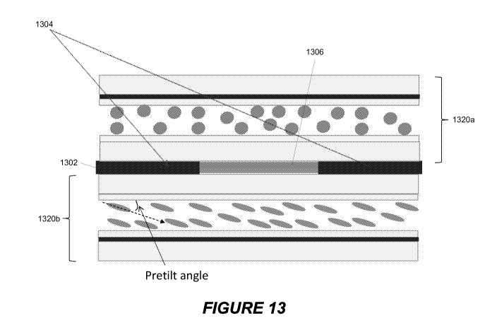
15 Figure 13 illustrates an additional variant of a tunable LC lens using a
hidden
electrode to provide spatial modulation of the electric field via frequency
tuning. In
Figure 13, the structure that controls the electric field gradient is composed
of a hole
patterned peripheral electrode 1304 of fixed (preferably low) electrical
resistance,
while the central disk-shaped region in the center of this electrode (on the
same plane)
20 and the area around that plane is filled by a frequency dependent material
1306. This
gradient control structure (GCS) 1302 is sandwiched between two LC cells
1320a,
1320b having directors (average orientation of long molecular axis of LC) in
the
orthogonal planes. For example, one of the directors might be in the XZ plane
with
the second director being in the YZ plane, the normal of the sandwich being
the Z
axis. In this embodiment, one of the traditionally used "internal" electrodes
of LC cells
is removed to allow the formation of the electric field gradient within the LC
layer. The
position of the GCS 1302 may be advantageously used to combine multiple
functions
for the GCS, such as electrode, heater, and sheet resistance (of frequency
dependent
material) or temperature sensor. The heater and the temperature sensor may be
used
together to help keep the temperature of the device at an optimal level.
Additional
patterning of the electrode 1304 could also be used to measure the electrical
properties of the material 1306, such as sheet resistance, which plays a
crucial role in
the formation of the electric field profile, and which might change part-to-
part over time
with aging. In this context, the GCS may be made in different forms and from a
CA 02727912 2010-12-13
WO 2009/153764 PCT/IB2009/052658
21
special alloy (e.g., Mo/Al) to perform these multiple functions. Providing the
layer that
determines the spatial modulation of the electric field in the middle of the
assembly
has the advantage that it equally affects the electric field in the layer or
layers below
the modulation layer as above. By providing a middle electrode, the separation
between electrodes is essentially halved, and in spite of the need to drive
two
electrode cells, the voltage and part-to-part variations are less significant.
In the above embodiments, the structure of the TLCL is essentially all flat,
namely, the
frequency dependent layer, electrode layer (ITO or the like), LC layer, etc.
are flat. The
electric field shaping is either a result of patterning the electrode layer or
the complex
impedance of the frequency dependent layer, or both. It is however possible to
use
other structural configurations to provide the electric field shaping.
By way of a non-limiting example, the dimensions of a variable focus flat
refractive
lens embodiment of the invention will be provided. It will be appreciated that
dimensions can vary greatly depending on design choice and the choice of
materials.
The cover substrate can be made of glass with a thickness of 50 to 100
microns. The
hole-patterned electrode can be made of an opaque metal such as aluminum, or
it can
be made of Indium Tin Oxide (ITO) which is transparent. The thickness of the
electrode can be in the range of 10 to 50 nm. The frequency dependent material
can
be made of titanium oxide with a thickness of about 10 nm. Titanium oxide has
semiconductor properties that change with control signal frequency.
The frequency dependent permittivity (or complex dielectric) material can
comprise a
variety of materials as set out in the following. The essential property of
such a
material is that it can exhibit a weak conductivity that will provide for
charge mobility
that is variable as a function of the frequency of the control signal. This
allows
frequency tuning of the shape of the electric field to control optical quality
or power, as
well as frequency tuning of the on/off operation of the LC optical device.
Top and bottom alignment layers can be polyimide layers of about 20 to 40nm
thick
that are rubbed to yield surfaces that induce a liquid crystal ground state
alignment
with a low angle pre-tilt. The layer of liquid crystal can be 5 to 30 microns
thick, as an
example. Such a single layer of liquid crystal with spatial modulation form a
gradient
index lens focuses a single linear polarization of light. In the embodiment of
Figure 13,
a hole-patterned electrode 1304 and frequency dependent material 1306 are
placed
on the top substrate, and this electrode is shared between two LC layers or
cells
1320a and 1320b.
CA 02727912 2010-12-13
WO 2009/153764 PCT/1B20091052658
22
It will be appreciated that a two to four layer TLCL can be assembled in this
manner
that can have a lens diameter of about 1 to 3mm with a thickness of about 460
microns. The optical power of the TLCL can be roughly from 8 to 16 diopters,
which is
suitable for most camera applications. One TLCL can provide variable focusing,
while
two can provide a zoom lens.
In the embodiment of Figure 14, two different frequency dependent materials
are
arranged to have a non-planar geometry. The different complex dielectric
constants of
the materials allow the shaping of the electric field as a function of control
signal
frequency to affect the effective 3D shape of the electrode. It is preferred
that the two
materials have their optical index of refraction matched, so that the non-
planar
geometry does not interfere with optical transmission and refraction, however,
a lens
system can also be designed to account for any effect of an electrode
structure that
would have an image altering effect.
In this embodiment, the two frequency dependent materials are located in the
same
layer, and occupy different regions of that layer. A first material 1406a has
a lens-like
shape and is centered relative to an optical axis of the lens. A second
frequency
dependent material 1406b occupies the remainder of the layer and has a
different
frequency dependent characteristic than the first material. Thus, as an
electric field is
applied to the layer, the response of the two materials 1406a, 1406b will be
different.
In this embodiment, both the upper electrode 1404 and the lower electrode 1423
are
planar and parallel to one another, with the liquid crystal 1421 in between.
As the
frequency of the voltage potential between the two electrodes 1404, 1423 is
changed,
the distribution of the electric field applied to the liquid crystal will
change. This allows
the optical characteristics of the LC cell 1420 to be changed by changing the
control
frequency, as the "shape" of the electric field will be dictated by the
relative location of
the two materials 1406a, 1406b and their relative permittivities.
If, for example, an excitation frequency used with the Figure 14 embodiment
was such
that the movement of charges was very limited, and the dielectric properties
of
materials 1406a and 1406b are similar, the electric field that is seen by the
LC layer
will be essentially uniform. This will result in a uniform reorientation of
the LC
molecules without any lensing effect and without disclinations. However, if a
frequency is applied for which the movement of charges is substantial in the
layer
1406b (but insignificant in layer 1406a), the electric field experienced by
the LC layer
will be stronger on the periphery, thus creating a gradient of reorientation
and
CA 02727912 2010-12-13
WO 2009/153764 PCT/IB2009/052658
23
corresponding lensing effect. Moreover, the transition between these two
states can
be done smoothly and without disclinations. This is an important advantage
provided
by frequency control of the field profile, one which is not possible to obtain
using only
voltage control that changes the amplitude of the excitation field but not its
profile.
Those skilled in the art will recognize that the relative shapes of the
materials 1406a,
1406b and their permittivities may be selected as appropriate to a particular
application. Moreover, a complex frequency dependent layer such as this may
make
use of more than two different frequency dependent materials. In addition, as
with
previous embodiments, a tunable lens using this construction may be tuned by
varying
the frequency of the drive voltage, or by varying the magnitude of the voltage
having a
particular frequency, or by a combination of both adjustments.
In the embodiment of Figure 15, a frequency dependent layer 1506 is provided
that
has a gradient of cross linking of a conductive polymer or gel, or another
frequency
dependent material, that provides a gradient of frequency-dependent charge
mobility.
This gradient structure can be created, for example, by a laser beam or other
light
(e.g., UV) or thermal source with gradient shaped intensity, a central drop
and
diffusion followed by polymerization, or a field induced (e.g. electrolytic)
material
separation followed by polymerization. In this embodiment, when the frequency
of the
voltage applied to the electrodes 1504, 1523 is very high, layer 1506 has
little effect
on the electric field, which appears as if generated by the uniform electrode
pair with
no such layer in between. That is, the effective upper electrode appears to be
at the
actual upper (top) electrode position. However, as the frequency is lowered,
the
frequency dependent material begins to experience a higher degree of movement
of
charges within certain regions of the material. As the frequency is lowered
further,
more of the material begins to experience charge movement according to the
gradient
structure. The shape of the gradient thus dictates the manner in which an
effective
electrode structure develops in the material 1506 and, correspondingly, how
the shape
of the effective electrode changes with frequency. Since the electrode shape
is
directly related to the profile of the electric field, this creates a
frequency tunable
electric field profile and, therefore, a frequency tunable effect on the LC
layer.
When the frequency is lowered enough that the frequency dependent permittivity
material is fully conductive, the effective upper electrode appears to be
located at the
bottom of the frequency dependent permittivity layer. Thus, the effective
electrode
follows a shape according to the gradient within the material 1506 when at a
CA 02727912 2010-12-13
WO 2009/153764 PCT/1B2009/052658
24
frequency that is between a low frequency at which the frequency dependent
layer is
fully "conductive," and a high frequency at which the whole frequency
dependent layer
is essentially "non-conductive." Thus, as with the embodiment of Figure 14,
the shape
of the electric field applied to the liquid crystal can be adjusted by
adjusting the
frequency of the electrode voltage.
Figure 16 illustrates an embodiment that combines the effect of a gradient
frequency
dependent layer 1606 (such as that shown in the embodiment of Figure 15) with
a
patterned electrode 1604. Those skilled in the art will understand that the
particular
shape of the electrode 1604 and the effective frequency dependent variability
of the
conductive layer 1606 may be selected to provide a desired range of electric
field
shapes when the frequency of the electrode voltage is adjusted. The material
1606
may be, for example, a material with a complex dielectric constant of gradient
form
(the gradient is indicated in the figure by dashed line 1607), and has a
different level of
frequency dependent charge mobility in different gradient regions. The
material 1606
may be constructed from one material with a gradient created therein, or from
a
combination of two or more materials. The material 1606 is adjacent to top
electrode
1604, while an LC layer 1621 is adjacent to a bottom electrode 1623. The
combination of the top electrode shape and the frequency dependent gradient
structure in the layer 1606 is used to produce a desired range of effective
electrode
shapes and, therefore, a desired range of electric field profiles.
Figure 17 illustrates another embodiment of the invention in which the
electric field
between planar upper and lower electrodes 1704 and 1723 is modulated by an
optically transparent hidden structure of having different frequency dependent
materials 1706a and 1706b, as well as a layer 1706c having a frequency
dependent
material with a gradient structure, like that of Figure 15. The frequency
dependent
characteristics of materials 1706a and 1706b are different, and create a
particular
effective electrode structure in their common layer that is dependent on an
applied
excitation frequency. In addition, frequency dependent shaping of the electric
field is
done by frequency dependent layer 1706c. One advantage of this approach is
that
light traverses the flat surfaces of materials 1706a and 1706b, but the
electric field
seen by the LC layer may be flat or curved depending the frequency of the
applied
excitation voltage. Notably, the specific shapes and positions of the
materials 1706a,
1706b, and the specific complex characteristic of the layer 1706c are selected
CA 02727912 2010-12-13
WO 2009/153764 PCT/IB2009/052658
according to a desired application. Those skilled in the art will recognize
that a wide
variety of different electric field shapes may be thereby created.
Figure 18 illustrates a further embodiment in which a frequency dependent
material is
arranged in a way to change the effective 3D shape of the electrode structure
as a
5 function of frequency. This embodiment combines the use of a shaped upper
electrode 1804 (in this case disk-shaped) and a frequency dependent layer that
includes a non-conductive area 1806a and a frequency dependent material 1806b.
By
carefully selecting the shape of the electrode 1804, the relative distribution
of the non-
conductive area 1806a and material 1806b, as well as the frequency dependent
10 characteristic of the material, a desired electric field shape may be
generated. Like
the embodiment of Figure 17, this embodiment benefits from the flat surfaces
of the
material layers, through which light easily propagates.
Figure 19A illustrates the equipotential lines of the electric field resulting
from the
electrode structure of Figure 18 at a relatively high frequency (in this case
10 kHz at
15 20V) at which the frequency dependent layer has only moderate charge
mobility. The
effective electric field shape in this instance appears as if generated by the
central
disk-shaped electrode, with no significant contribution from the frequency-
dependent
material. Figure 19B illustrates the equipotential lines of the electric field
resulting
from the electrode structure of Figure 18 at a relatively low frequency (in
this case 100
20 Hz at 20V) at which the frequency dependent layer exhibits significantly
more charge
mobility. The effective electric field shape in this instance appears as if
generated by
the central disk-shaped electrode on the top of the electrode structure along
with a
ring electrode located at the bottom of the frequency dependent permittivity
layer. It
will be understood that at intermediary frequencies, the effective electrode
shape will
25 be smoother, and somewhat dome-shaped.
Figure 20 is an embodiment having somewhat of an opposite geometry with
respect to
the embodiment of Figure 18, with Figures 21A and 21 B showing the
corresponding
equipotential lines for different driving frequencies, essentially as in
Figures 19A and
19B. Whereas the Figure 18 embodiment uses a disk-shaped electrode and a
central
region in the frequency dependent layer that is non-conductive, the Figure 20
embodiment uses a hole-patterned electrode 2004 and a frequency dependent
layer
2006 for which the conductive material is all located in a center region below
the "hole"
of the electrode. This embodiment may therefore be used to create an electric
field
response that is somewhat opposite to that of Figure 18. Such a geometry can
be
CA 02727912 2010-12-13
WO 2009/153764 PCT/IB2009/052658
26
useful, for example, for creating a tunable LC lens that may be changed from
positive
to negative in response to changing frequency. At a high frequency (e.g., 12
kHz at
25V), the frequency dependent material has no significant charge mobility, and
the
electric field appears as if generated by just the hole-patterned electrode.
At low
frequency (e.g., 200 Hz at 25V), the frequency dependent material has a much
higher
charge mobility, so the electric field appears as if generated by the
electrode 2004 and
a disk-shaped electrode located at the bottom of the frequency dependent
material.
Changing the frequency between these extremes creates a smooth range of curved
electric field shapes suitable for tuning an LC lens. Thus, a lens with both
positive and
negative tenability is provided.
It is important to note that many other variant configurations of an LC lens
using such
a hidden electrode to provide for modulation of the electric field are
possible and are
included within the scope of the present invention.
Frequency-dependent material
As mentioned above, the present invention provides various chemical
compositions of
a frequency dependent material, suitable for use in tunable optical devices,
such as
the LC lenses described herein. Those skilled in the art will recognize that
such
materials may also be used in other frequency-dependent optical applications,
such as
beam steering devices, shutters, and the like. A uniform or non-uniform layer
of the
frequency dependent material may be incorporated into the lens, beam steering
device, and/or shutter configuration, in order to provide for spatial
modulation of an
electric field via frequency tuning. Thus, tuning can be frequency controlled.
Such a
device may be used for tunable focusing, diffracting, steering, and the like.
For the different LC lens configurations discussed above, the frequency
dependent
layer is made of a material having a complex dielectric permittivity which is
dependent
(including the weakly conductive properties) on a driving frequency applied to
the
system electrodes. According to a non-limiting example of implementation, this
material may be a thermally or photo polymerizable conductive material, whose
composition may include the following elements:
(i) a polymerizable monomer (linear or cyclic) compound;
(ii) an initiator;
(iii) an additive to change the dielectric constant or conductivity of the
final
composition;
CA 02727912 2010-12-13
WO 2009/153764 PCT/1B2009/052658
27
(iv) an adhesive to increase the adhesion of the polymer to a glass surface
(the
adhesive may be used as surface treatment agent or incorporated directly to
the
solution to increase the adhesion); and
(v) a filler to change the viscosity of the mixture.
In one example, 90 (wt.) of isodecyl acrylate (SR256) is mixed with 0.3%
Li+CLO4-
(wt%). Then 3% of an initiator; 2-hydroxyl 2-methyl 1,1 - phenyl propanone
(Darocure
1173) is added and the mixture stirred carefully at room temperature to obtain
a
homogeneous clear solution. Then a quantity of 10% of ECA (2-ethyl
cyanoacrylate)
(wt% of total mass of the monomers) was added and the final solution stirred
carefully
for 15 minutes at room temperature and dark conditions. The mixture can be
polymerized by a UV source by exposing the material for three minutes at an
intensity
of 15 mV/cm2.
In another example, in order to prepare a first part of the composition, 35 %
(wt.) of
optical adhesive OA9352HT2 (HT) is mixed with 65 % (wt.) of (2(2-Ethoxyethoxy)
Ethylacrylate monomer) and the mixture is stirred carefully at room
temperature to
obtain a homogeneous clear solution. Then a quantity of 10 % of 4-
methylphenyl)[4-
(2-methylpropyl)phenyl]-hexafluorophosphate (wt. of total mass of the
monomers) is
added and the final solution is stirred carefully for 15 minutes at room
temperature and
dark conditions.
A second part of the composition having low epsilon or conductivity is a 55%
wt. of
isodecyl acrylate (SR395) mixed with an optical adhesive (45% wt., AT6001).
The
solution is stirred carefully for 15 minutes at room temperature and dark
conditions.
The mixture can be polymerized by an UV source by exposing the material for 3
minutes with an intensity of 15 mV/cm2. Optionally, an optical elastomer from
the
silicone family may be included in the thermal- or photo-polymerizable
conductive
material and used as a low epsilon part of the composition. This material may
be
classed as a thermally curable compound (and may be a one or two part silicone
elastomer).
It should be noted that various material compositions, various LC layers,
various
electrodes, various director alignments, various geometrical forms, etc. may
be used
to fabricate the same optical device. That is, different combinations of
materials and
physical structures disclosed herein may be used for a particular application,
although
the use of a frequency dependent material, which allows for frequency tuning
of the
optical device, is common to each of these embodiments.
CA 02727912 2010-12-13
WO 2009/153764 PCT/1B2009/052658
28
It has been determined that various different chemical compositions of a
material with
complex dielectric permittivity may be suitable for use in the above-described
frequency tunable lens, beam steering device, and/or shutter configurations,
where
this material may be altered (including the weakly conductive properties) by
modulating a driving frequency applied to the electrodes.
According to one embodiment of the present invention, the
polymerizable monomer compound has at least one ethylenically unsaturated
double
bond and has a complex dielectric constant including an imaginary part which
describes the conductivity, and the initiator is a combination of UV-Vis, NIR
sensitive
or thermally sensitive molecules.
On particular initiator compound may include, for example, mixed
triarylsulfonium
hexafluoroantimonate salts, hexafluorophosphate salts, and any other suitable
initiators known to those skilled in the art. A preferred initiator compound
is 4-
methylphenyl [4-(2-methylpropyl )phenyl]-hexafluorophosphate.
The additive to change the dielectric constant or conductivity of the thermal-
or photo-
polymerizable conductive material may be an organic ionic compound (such as
iodonium (4-methylphenyl)[4-(2-methylpropyl)phenyl]-hexafluorophosphate or
triarylsulfonium hexafluoroantimonate salts, mixed in propylene carbonate),an
inorganic ionic compound (such as Li+CIO4-, K+CIO4- etc.), an ionic
organometallic
compound, or a mixture of any of these, and any other suitable additives known
to
those skilled in the art.
The adhesive is sensitive to UV-Vis, NIR, or is an adhesive that is
polymerized using a
thermal initiator and may be used as surface treatment agent, or incorporated
directly
to the solution to increase the adhesion. In the example above, the adhesive
is optical
adhesive OA9352HT2 (HT), but other suitable adhesives will be known to those
skilled
in the art.
The optical elastomer, as discussed in the example above, may be selected from
a
group including isodecyl acrylate (SR395) mixed with an optical adhesive
(AT6001),
and any other suitable optical elastomers known to those skilled in the art.
According to another embodiment of the present invention, the frequency
dependent
material is a high dielectric constant liquid, chosen from all transparent
liquid materials
having an epsilon value between 2.0 and 180.0 able to provide for charge
mobility.
Preferably, the high dielectric constant liquid has an epsilon value between
30.0 and
150Ø More preferably, the high dielectric constant liquid has an epsilon
value
CA 02727912 2010-12-13
WO 2009/153764 PCT/IB2009/052658
29
between 60.0 and 120Ø The liquid may be pure, or a mixture of alkylene
carbonates
family, such as propylene carbonate (PC) or glycerin carbonate (GC) having
epsilon of
67 and 111, respectively, alkyl group, a substituted alkyl group, an alkyl
carbonyl
group, an alkoxycarbonyl group, an aryl group, a substituted aryl group and an
aryl
carbonyl group. Furthermore, use of water, glycerol, and mixtures of water
with an
organic or inorganic compound such as glycerol, alkaline salts, or rare earth
alkaline
salts are also envisioned. One particular example is a mixture of 7% distilled
water
with 93% glycerol. The solution is stirred for fifteen minutes at room
temperature (the
refractive index of the solution is adjusted to a value of 1.4630 that is
compared to the
second part of the hidden layer).
According to another embodiment of the present invention, the frequency
dependent
material is an electrolyte gel, which includes a polymer material (used as a
matrix), an
ionic composition, and an ion transporter.
In general, all commercially available polymers (such as polyacrylic, epoxy
material,
polyurethane, polycarbonate, and polyphenylic material) which are miscible
with the
ionic composition and ion transporter material can be used as polymer matrix.
The
ionic composition having the anion and cationic species may be selected from
the
group including soluble alkaline or rare alkaline salts (such as Li+, K+,
etc.), organic, or
organometallic compound.
The ion transporter material may be a pure liquid such as propylene carbonate
(PC),
ethylene carbonate (EC) or a mixture of two or more liquids or a monomer
having a
polar group such as etheric or phenoxy group. This polar group can be a side
chain or
may be incorporated in polymer's main chain. For example: (2(2-ethoxyethoxy)
ethylacrylate monomer), in which the etheric group is a long side chain and
plays a
role of ion transporter. An example of an electrolyte gel might be 10% wt. of
PMMA
dissolved in 80% propylene carbonate (PC). The solution is stirred over night
at room
temperature. Then a quantity of 10% wt. 'of Li+CIO4- is added to the solution
and
stirred at room temperature. The final gel like material is used as the high
dielectric
constant layer part of a tunable LC lens.
According to a further embodiment of the present invention, the frequency
dependent
material may be a conductive ionic liquid. This material is classed in
different organic,
inorganic or organometallic compounds having the ionic species such as
chlorate,
perchlorate, borate, phosphate and carbonate. Specific, non-limiting examples
of
CA 02727912 2010-12-13
WO 2009/153764 PCT/IB2009/052658
such materials include (1-butyl-3-methylimidazolium tetrafluoroborate) and (1 -
butyl- 3-
methyl imidazolium hexafluorophosphate).
Yet another example of the frequency dependent material is an electronic
conductive
polymer. The most important aspect of conjugated polymers is their ability to
act as
5 electronic conductors. These materials range from conventional polymers
(e.g.,
polythiophene, polyaniline, polypyrrole, poly acetylene) or PEDOT poly(3,4-
ethyl enedioxythiophene) and PEDT from Clevios to new polymers with
specialized
conductivity properties such as low band gap and intrinsically conducting
polymers.
In a nano particle environment, materials may be dispersed in water, an
organic
10 solvent, monomer. For example, ATO ((Sn02)o.9(Sb2O5)0.1) dispersed in the
water or
in the polyethylene glycol diacrylate, or the nano particle used in a powder
form
coated by sputtering as a thin layer on the substrate. Or the carbon nanotubes
(CNTs) that are allotropes of carbon with a cylindrical nanostructure. This
material
may be used as dispersed nanoparticles in the water or an organic material
such as a
15 monomer. The nanoparticles can be deposited by different techniques such as
spin
coating process on the surface of the glass.
Another possibility for preparing the frequency dependent layer is based on
the
deposition of metallic oxide as a thin film on the surface of a glass
substrate. In this
case, the metallic compound is deposited on the surface of the glass followed
by an
20 oxidation process. In this method, a metallic target is used for e-beam,
sputtering or
thermal evaporation process. For example, metallic oxide compounds such as
Sn02,
Ti305, ZnS, Zn02, etc. prepared by e-beam technique can be used as a frequency
dependent portion.
Conductive glass can also be used as a frequency dependent portion of a
tunable LC
25 lens. In this case, the conductive material can be doped in glass (bulk)
and used as a
target in a thin film deposition technique (such as e-beam, sputtering or sol-
gel
process, etc.). Examples include molybdenum, silver or a mixture of them doped
directly into the glass and used as conductive glass target for thin film
deposition
technique. While a Ti305 (titanium oxide) layer may be about 10 nm thick, a
polymer
30 that provides some ionic conductivity can work well, although the thickness
would be
in the range of 0.1 to 30 microns.
Driving Signals
CA 02727912 2010-12-13
WO 2009/153764 PCT/IB2009/052658
31
The specific materials used herein to provide frequency-dependent control of a
corresponding optical device may make use of a variety of different driving
signals
having different characteristics. These signal characteristics include
frequency
variations, and may also include amplitude and duty cycle control. Some
examples of
these are discussed in more detail below.
Pulse-width modulation
One way of doing frequency control is by using a signal with so-called "pulse
width
modulation" (PWM). Figure 22 illustrates the parameters of a PWM signal,
namely
amplitude, period and duty cycle or fill factor ("FF"). As shown, the PWM
signal has a
characteristic defined by the total period, and the duration of the pulses
determines
the duty cycle. The frequency domain characteristics of the PWM signal are
shown
schematically in Figure 23, which indicates the frequency content of a PWM
waveform
for different fill factors. It will be appreciated that a pulse train contains
a dominant
frequency corresponding to the waveform period. However, as the Fourier series
for
such a waveform demonstrates, higher frequency components of lower amplitude
are
contained in a square wave. Thus, while most of the energy of a 50% duty cycle
square wave pulse train is contained in the "central" frequency corresponding
to the
PWM signal period, some energy is still carried in other frequencies. This is
demonstrated by the fill factor shown in the "high FF" envelope indicated in
Figure 23.
In the case of lower fill factors, the amount of energy in the PWM signal away
from the
central frequency is greater. This corresponds to a broader envelope that has
more
energy in the higher frequencies. In the case of higher duty cycles, the
amount of
energy in the PWM signal away from the central frequency is less. As an
example,
changing a PWM duty cycle from 50% duty cycle down to 5% would change RMS
voltage by an order of magnitude from a normalized 1.0 down to 0.1, while at
the
same time causing a significant increase in the energy at higher frequencies.
The control of a TLCL may make use of PWM, for example, in certain
applications
such as lenses for cell phone cameras. PWM control provides certain advantages
for
such a TLCL and may be seen as having the following characteristics:
1) For a given "central" frequency, e.g., f=f1, the driving "maximum
amplitude"
may be set such that a maximum of optical power is achieved at relatively low
FF taking into account that the real spectra of driving signal will be
significantly
broadened. Then, simply increasing the FF will increase the RMS voltage and
CA 02727912 2010-12-13
WO 2009/153764 PCT/IB2009/052658
32
thus will decrease the optical power, but this decrease will not follow the
curve
for f1 (Figure 24A). In fact, due to the increase of FF, the spectral content
of the
driving signal will be significantly reduced, thus, the optical power will be
reduced not only because of the growth of the RMS voltage but also because of
the decrease of high frequency signal components. This will bring a much
"faster" decrease of optical power, allowing the use of comparatively low
voltages.
2). Once the maximum optical power is achieved for a given driving frequency
and FF, the driving frequency can be shifted down, effectively changing from
one transfer function to another (such as changing from f, to f2 in Figure
24A).
This helps avoid the need for high RMS voltages to bring the optical power of
the lens to a minimum.
3). Combined or simultaneous FF and frequency changes can also be used to
achieve optical power control. The present invention is directed to a tunable
LC
lens using a hidden electrode system to provide spatial modulation of the
electric field via frequency tuning. Thus, tuning of the lens can be frequency
controlled, although adjustment of the FF also changes the relative frequency
content of the driving signal. As such, both FF and frequency can be used to
tune the lens. As mentioned above, the devices of the present invention may
be used for a variety of different applications, including tunable focusing,
diffracting, steering, etc.
In contrast to PWM mode, amplitude modulation (AM) mode may also be used to
modulate the lens given a particular frequency. Figure 24A schematically
demonstrates the transfer functions showing RMS voltage versus optical power
for
different driving frequencies f1-f3 in the Amplitude Modulation mode.
Different options
of control are possible with the proposed TLCL in both amplitude modulation
(AM) and
PWM mode. AM mode differs from PWM mode in that the PWM signal relies on
control of the RMS amplitude by changing the filling factor to determine the
relative
high or low frequency content of the signal. In contrast, AM uses a set
frequency
signal with 100% fill factor and changes only the amplitude of it. The
different curves
in Figure 24A show how, for different selected frequencies, RMS voltage can be
used
to change optical power of a TLCL. Such behaviour is typical, e.g., for the
lens shown
in Figure 14.
CA 02727912 2010-12-13
WO 2009/153764 PCT/IB2009/052658
33
Figure 24B is similar to Figure 24A, but shows how a frequency controlled lens
would
behave for different control voltages. For the different voltages shown, the
increase in
frequency corresponds to an increase (and subsequent decrease) in the optical
power
of the lens. However, depending on the voltage, the optical power may have a
higher
maximum, and that maximum may occur at a higher frequency. Such behaviour is
typical, e.g., for the lens shown in Figure 5.
The control signal for tuning the optical device can be provided by a variable
frequency control signal circuit configured to cause said device to control
propagation
of light in the device as a function of control signal frequency. As an
example, in
Figure 25, there is shown schematically a camera having a LC lens 2502
combined
with at least one fixed lens 2504 to focus an image onto an image sensor 2506
with
the LC lens 2502 providing focus control. The image is fed to a camera
controller 2508
that includes an autofocus function that outputs a desired focus value. An
electric field
controller 2510, typically using lookup tables (with possible/optional
information about
the geometry, material, temperature, sheet resistance, camera, etc.),
translates the
focus value into an electrical parameter, in this case a desired fill factor.
In the case
that tuning cannot be achieved only by the fill factor setting at a single PWM
waveform
amplitude and period, the controller 2510 can adjust a PWM amplitude setting
and
period setting. The PWM drive circuit 2512 itself may be a conventional PWM
circuit.
Those skilled in the art will appreciate that components 2508 and 2510 can be
implemented using microcode executed on a microcontroller, while component
2512
can comprise voltage sources switched under the control of the microcontroller
to
pulse width modulation circuitry also controlled by the microcontroller to
have a
desired frequency and duty cycle.
In the case that the frequency content is to be controlled to reduce the
presence of the
higher frequencies, the PWM amplitude can be stepped down while the duty cycle
is
then increased to achieve the same RMS voltage as a mechanism to avoid the
creation of the higher frequencies that the electrode system or the LC cell
will respond
to in an undesirable manner.
Complex Frequency Signals
Although PWM or AM signals are specifically discussed above, it is possible to
use a
driving signal that is simply carried on one frequency or is the combination
of multiple
individual frequency components. Such a "complex frequency" signal can be, for
CA 02727912 2010-12-13
WO 2009/153764 PCT/IB2009/052658
34
example a combination of individual signals at different frequencies all mixed
together
in a predetermined ratio (but dynamically variable). Unlike the PWM method,
the
complex frequency signal does not rely exclusively on square wave type signal
shapes, and does not use an adjustment of filling factor to change the level
of high
and low frequency components.
Figure 26 illustrates how three control signals of three different frequencies
can work
together to shape the electrode voltage profile for a frequency tunable lens
structure
such as that of Figure 25, where the complex frequency signal generator would
replace the PWM signal generator 2512 shown in that figure. Referring again to
Figure 26, the figure shows an effective voltage across a LC lens with a
center point of
an electrode radial position shown in the center of the range. The values for
amplitude and frequency used in this description are just for example.
A first signal of 100Hz at 10V is active to reduce disclinations across the
lens, as it
produces very little variation in effective voltage relative to radial
position. A second
signal of 3kHz at 12V provides a general shape to the lens. Finally, the third
signal of
20kHz at 8V contributes to the overall voltage profile in a manner that
improves the
lenticular (spheric or aspheric) properties of the profile. Thus, the
combination of the
three signals shape the electrode voltage profile in a way that is better than
a single
frequency. The first signal can be used to ensure that the whole aperture of
the LC
layer is subjected to a minimum voltage to begin orientation of the LC
molecules. The
second signal has a smooth transition between the outside and the center, and
provides a good smooth profile. The addition of a third signal at a higher
frequency
may provide a more spherical, lenticular, aspheric or other desired profile.
Those skilled in the art will recognize that the addition of more signals at
other
frequencies can be used to further shape the electric field in a way that is
desirous for
the lens properties. In addition, once a desired voltage profile is achieved,
tuning of
the lens can be done also by voltage adjustment alone. Voltage adjustment can
be
done for all signals together, or a different adjustment can be used for each
of the
different frequencies.
Shaped Electrodes
Figure 27A schematically illustrates a tunable LC lens according to the
present
invention that uses a geometrically shaped fixed electrode. As shown, a layer
of LC
2702 is sandwiched between top and bottom substrates 2713 and 2724,
respectively.
CA 02727912 2010-12-13
WO 2009/153764 PCT/IB2009/052658
A flat bottom electrode 2708 (which may be a layer of ITO) is provided on the
bottom
substrate, and is coated by an orienting coating 2710 (e.g., rubbed polyimide)
for
aligning the LC molecules of the LC layer 2702 in a predetermined direction.
The
surface of the top substrate that is adjacent the LC layer is also coated with
an
5 orienting coating 2710 for aligning the LC molecules. In addition to the
bottom
electrode 2708, the electrode system includes a top electrode structure 2712
that is
formed of a lens-like polymer structure 2714 coated by a curved electrode 2716
(which may also be an ITO layer). The top electrode structure 2712 is a
combined
variable electrode structure (CVES) and also includes a layer 2706 of material
having
10 a frequency dependent complex permittivity. Although not necessary, this
may be an
index matched layer with variable conductivity (IMLVC)), where this material
is
arranged between the top substrate of the LC cell 2713 and the lens-like
polymer
structure 2714. The permittivity of this material, and thus the charge
mobility, may be
changed dynamically (e.g. by a change of drive frequency in a voltage applied
15 between the top and bottom electrodes).
The frequency dependent material may be a weakly conductive material such as
those described above, whose charge mobility is variable as a function of an
electrical
signal frequency applied to the electrodes, such that it can be used to
spatially
modulate the electric field resulting therefrom. More specifically, the weakly
20 conductive material may be a complex dielectric material having a
permittivity/conductivity that is dependent on frequency. Therefore, by
varying the
frequency of the AC excitation voltage between the electrodes 2708 and 2716,
one
can vary the degree of charge mobility in the frequency dependent layer. This
provides for a variable (frequency controllable) transformation/adjustment of
the
25 electrical field that is generated in the LC cell by the bottom flat and
top curved
electrodes.
In the present embodiment, the form of the lens-like polymer structure of the
top
electrode structure can be selected to optimize its optical function while its
electrical
function (generating the electrical field in the LC cell) can be adjusted by
the flat
30 IMLVC layer and the choice of the driving frequency. Furthermore, the
curvature of
the electric field generated in the LC layer may be changed from a lens-like
form at a
relatively high driving frequency to a flat electric field distribution at a
low driving
frequency (as if, effectively, one were using two flat electrodes). That is,
the high
charge mobility state of the frequency dependent layer, which results from the
low
CA 02727912 2010-12-13
WO 2009/153764 PCT/IB2009/052658
36
drive frequency, makes the top structure appear as if the curved electrode did
not
exist and as if the layer 2706 was the top electrode. Accordingly, it is
possible to
avoid the generation of disclinations (abrupt orientation changes in space).
Finally,
the transformation of the electric field profile by the dynamic reorientation
of LC
molecules (and corresponding aberrations) may be compensated by the dynamic
change of the charge mobility of the hidden layer of the frequency dependent
material,
which will reshape the profile of the electric field.
Alternatively, for relatively high driving frequencies, where the movement of
charges is
very limited in material 2706, the profile of the electric field will not be
affected, and will
be defined primarily by the curvature of the lens like polymer structure 2714.
In a
variation of this embodiment, the lens like polymer structure may be
fabricated from
the same material as the layer 2706. The operation of such a structure will be
very
similar to that defined above, but there will be no need of a separate layer
of material
2706.
Although the layer of frequency dependent material is described in the given
examples
as being a part of the electrode system of the tunable LC lens, it may also be
considered as being separate from the electrode system, simply as an
additional
element of the tunable LC lens. As part of the lens, it allows for the shape
of the
electric field generated by the electrode system to be dynamically controlled
by
varying a frequency of a drive signal applied to the electrode system.
Figure 27B shows the electric equipotential planes of the LC lens shown in
Figure
27A, for a high driving frequency (in this case, 100 kHz at 35 Vrms). By
applying a
high frequency driving signal, the charge mobility of the hidden layer (IMLVC)
is
minimized. This low charge mobility state allows the creation of a gradually
varying
electric field within the LC layer, corresponding to a spatially non-uniform
reorientation
of the LC molecules and a non-uniform refractive index distribution in a lens-
like form
(i.e., the LC lens becomes tunable).
Figure 27C shows the electric equipotential planes of the LC lens shown in
Figure
27A, for a low driving frequency (in this case, 100 Hz at 35 Vrms). By
applying a low
frequency driving signal, the charge mobility of the hidden layer (IMLVC) is
maximized. This high charge mobility state allows the creation of a uniform
electric
field within the LC layer, corresponding to a spatially uniform reorientation
of the LC
molecules and a uniform refractive index distribution. It is therefore
possible to start
the reorientation process with such a uniform excitation, in order to avoid
the formation
CA 02727912 2010-12-13
WO 2009/153764 PCT/IB2009/052658
37
of disclination defects, after which the driving frequency can be adjusted to
higher
values to form the lens-like structure. The frequency of the driving signal
can then be
adjusted to come back to the uniform excitation, in order to gradually remove
the lens-
like structure without going to the ground state (V = 0 volt), which is
usually very slow.
It should also be noted that, during the reorientation of the LC molecules,
the profile of
the electric field (within the LC layer) will be changed. However, the LC lens
configuration shown in Figure 27A allows for the correction of any undesired
transformations of the electrical field by adjusting the frequency and the rms
voltage of
the driving signal, thus keeping the lens aberrations below the desired value
(which
could not be done with fixed pairs of electrodes). It should be understood
that the use
of a frequency dependent layer and frequency control enable a unique
possibility of
"reconciling" the optical functions (with good "fixed" optical power and low
aberrations)
of the element 2714 with the generation of a good profile of electric field
(seen by the
LC) using electrode 2716 and frequency dependent layer 2706.
Figure 28A schematically illustrates a variant configuration of a tunable LC
lens
according to the present invention. As seen in the figure, the shape of the
lens-like
polymer structure 2814 that is arranged on the top substrate 2813 and coated
by a
curved electrode 2816 (which may be an ITO layer) differs from that of Figure
27A.
The top electrode structure still includes a layer 2806 of material having a
frequency
dependent permittivity, where this material is arranged between the top
substrate
2813 of the LC cell and the lens-like polymer structure. Accordingly, the lens
shown in
Fig. 28A has a similar operation as that of the lens of Fig. 27A, but with the
opposite
tunability. That is, the effective electric field shape induced by the
structure creates an
opposite lensing effect to that of Figure 27A, allowing the optical power of
the lens to
be modified in an inverse sense with changes in the drive frequency. This
opposite
tenability may be desirable in certain lens applications.
Figure 28B schematically illustrates another variant configuration of the
tunable LC
lens, according to the present invention. In Figure 28B there is shown a LC
lens
configuration in which a layer of LC 2802 is sandwiched between top and bottom
substrates 2813, 2824. A flat bottom electrode 2808 (e.g., an ITO layer) is
provided
on the bottom substrate, coated by an orienting coating 2810 (e.g., rubbed
polyimide)
for aligning the LC molecules of the LC layer 2802 in a predetermined
direction. The
surface of the top substrate 2813 that is adjacent the LC layer is also coated
with an
orienting coating 2810 for aligning the LC molecules. In addition to the
bottom
CA 02727912 2010-12-13
WO 2009/153764 PCT/1B2009/052658
38
electrode, the electrode system includes a top electrode structure 2811 that
is formed
of a non-uniform "flat aperture" polymer (or other) structure 2815 coated by a
non-
uniform flat-surface electrode 2817 (e.g., an ITO layer), where this top
electrode
structure is arranged on the top substrate 2813. The top electrode structure
2811 also
includes a planar layer 2806 of frequency dependent material, where this
material is
arranged between the top substrate of the LC cell and the "flat aperture"
polymer
structure.
The choice of the "flat aperture" shape for the polymer structure means that
the top
electrode structure 2811, and thus the electrode system in its entirety,
becomes
optically "invisible," such that this layer no longer performs an optical
function (lensing)
and is solely responsible for the electrical function (generating a spatially
non-uniform
electric field in LC layer). As in the previously discussed lens
configurations, the flat
IMLVC layer and the choice of driving frequency provide for adjustment of this
electrical function, such that tuning of the LC lens is frequency
controllable. Another
important advantage arising from the fact that all of the surfaces in the LC
lens
configuration of Figure 28B are flat is that coating of the polymer structure
with a
uniform ITO layer can be done without difficulty.
Figure 28C schematically illustrates yet another variant configuration of the
tunable LC
lens according to the present invention. The configuration shown in Figure 28C
is
similar to that of Figure 28B, in that all of the surfaces of the combined
variable
electrode structure are flat. Accordingly, the lens configuration shown in
Figure 28C
provides for the same de-coupling of the optical and electrical functions of
the
electrode system, as well as for the same operational advantages, as discussed
above with regard to Figure 28B. However, this structure differs from that of
Figure
28B in that the position of the surfaces are reversed such that the electrode
2819 is
further from the LC layer in the center of the structure than it is near the
outside of the
lens. This creates a frequency tunable lens, like that of Figure 28B, except
that it has
an opposite optical tunability. That is, the optical power versus frequency
curve of the
lens of Figure 28C is opposite to that of Figure 28B.
Figure 29A schematically illustrates still another variant configuration of
the tunable LC
lens according to the present invention. As shown, a layer of LC 2902 is
sandwiched
between top and bottom substrates 2913, 2924. A flat bottom electrode 2908
(e.g., an
ITO layer) is provided on the bottom substrate 2924, and coated by an
orienting
coating 2910 (e.g. rubbed polyimide) for aligning the LC molecules of the LC
layer in a
CA 02727912 2010-12-13
WO 2009/153764 PCT/IB2009/052658
39
predetermined direction. The surface of the top substrate 2913 that is
adjacent the LC
layer 2902 is also coated with an orienting coating 2910 for aligning the LC
molecules.
Specific to the present embodiment, the top electrode structure 2912 of the
electrode
system includes a curved layer 2916 of variable permittivity material (IMLVC)
encased
in a flat-top layer 2914 of polymer (or other) material, which is arranged on
top of the
top substrate. As discussed above, the charge mobility of the IMLVC material
may be
changed dynamically (e.g., by the change of driving frequency). The top
electrode
structure also includes a flat and optically transparent layer 2906 (e.g., an
ITO layer),
which is arranged on top of the flat-top layer of polymer material.
Accordingly, in the variant configuration shown in Figure 29A, it is the
curved layer
2916 of weakly conductive material that operationally replaces the top curved
ITO
layer of Figure 27A. The form of the lens-like structure is not restricted
since it is
optically hidden and it has only one function: generating a non-uniform
electric field.
Furthermore, there are no curved surfaces to be coated by ITO. Optically
transparent
glue (with variable conductivity) is used to attach the replicated surfaces
(with
opposed but same/matching curvature) of the polymer structure with encased
curved
IMLVC. Also, the curvature of the electric field generated in the LC layer
2902 may be
changed from a lens-like form at low driving frequency (when the IMLVC is in
the high
charge mobility state) up to obtaining a flat electric field distribution at
higher driving
frequency (when the charge mobility of the IMLVC is very small, in which case
it
becomes a thin layer of simple dielectric, where even index matching is
unnecessary
(unless it is desired to reduce Fresnel reflection losses), thus avoiding the
generation
of disclinations (abrupt spatial orientation changes). Finally, the
transformation of the
electric field profile by the dynamic reorientation of LC molecules (and
corresponding
aberrations) may be compensated by the dynamic change of the charge mobility
of
the hidden layer, which will reshape the profile of the electric field.
Figures 29B and 29C show the maximum angle of reorientation of the LC
molecules in
the lens at high and low driving frequency, respectively, for the lens
configuration
shown in Fig. 29A. The output shown in Figure 29B (no lensing effect) was
produced
using a driving voltage of 40V at 100 kHz, while the output shown in Figure
29C was
produced using a driving voltage of 40V at 100 Hz (with lensing effect).
Figures 30A and 30B, respectively, illustrate two examples of different types
of
conventional LC cells that could be used in the LC lens configurations
described
above. In particular, Figure 30A shows a "pi" type cell and Figure 30B shows a
"twist"
CA 02727912 2010-12-13
WO 2009/153764 PCT/IB2009/052658
type cell. Other types of LC alignment, including hybrid alignments may be
considered too.
Figures 31A and 31 B illustrate, respectively, two possible configurations
combining
the novel electrode structure of the present invention with LC cells in order
to handle s
5 and p polarizations of light. In the configuration of Figure 31A, two liquid
crystal cells
(LCCX and LCCy) are oriented in the cross directions to handle the
perpendicular light
polarizations, and a CVES is located to either side of the LCC layers. In this
example,
each of the CVES layers is used to control a different one of the LCC layers.
The
alternative configuration of Figure 31 B is similar, but uses only one
electrode structure
10 to control two cross oriented LCCs. In this case, the bottom flat electrode
of the top
LCCx is oriented such as to allow the creation of the control electric field
by the top
electrode structure and the bottom flat electrode of the LCCy. It is also
possible to use
a configuration as shown in Figure 31 C, for which the CVES layer is adapted
and
located in the middle of the final device (between two cross oriented LC
cells).
15 Any of the frequency dependent materials discussed herein may be used in
the
different LC lens configurations above. Such materials have a complex
dielectric
permittivity that may be varied (including the weakly conductive properties)
by the
change of driving frequency. The specific characteristics of the material may
be
selected according to the particular lens structure in question. It should be
noted that
20 various material compositions, various LC layers, various electrodes,
various
geometrical forms, etc. may be used to fabricate the above-described LC lens,
without
departing from the scope of the claimed invention. It should also be
appreciated by
the reader that various optical devices can be developed using the LC lens
described
herein. In addition, all of the "curved" surface geometries discussed herein
(e.g.,
25 Figures 27, 28A) may be covered, or "filled," with optional passive
materials with the
same optical properties as the top surface to eliminate their purely optical
role, as
shown in Figure 29A.
Those skilled in the art will also recognize that certain devices may make use
of
materials that have low, or no, frequency dependence, but that may still be
"sensitive"
30 to the frequency of the excitation signal. This is the case where the
combination of
different elements provides electric field attenuation (in the transverse
plane)
depending upon the frequency, such as in distributed RCL electronic circuits.
Doped LC Layer
CA 02727912 2010-12-13
WO 2009/153764 PCTIIB2009/052658
41
Shown in Figure 32A is another alternative embodiment of the present
invention. In
this embodiment, a frequency dependent material separate from the LC layer is
absent and, instead, a LC material 3202 is used that itself has the desired
frequency
dependent properties. Although the frequency dependent material is part of the
liquid
crystal itself, the desired shaping of the electric field within the LC layer
is achieved. A
hole patterned conductive ring 3204 serves as the top electrode while a planar
bottom
electrode 3223 is located to the other side of the LC layer 3202. Oriented
coatings
3222 may be of rubbed polyimide and the structure has top and bottom
substrates
3213 and 3224, respectively. In this example, the structure uses an optional
mid layer
3225 which has the effect of additionally shaping the electric field created
by
electrodes 3204 and 3223. Another embodiment, shown in Figure 32B, is
essentially
the same, but has no such mid layer. In this embodiment, the electric field
(created
with the hole patterned electrode) is softened by the charge mobility of the
LC layer,
thus allowing the creation of a field that would generate a lens-like
refractive
distribution in spite of the close position of the hole patterned electrode to
the LC
layer. As illustrated in the results of Figure 33, the shaping of the electric
field from a
patterned electrode is significant when a liquid crystal having charge
mobility is used.
The simulation of equipotential lines presumes using a reltively standard ITO
electrode
layer (<100 kQ/sq) in the area between the hole patterned electrode in
combination
with a weakly conductive liquid crystal having conductivities on the order of
10"3 S/m.
The annular electrode of Figures 32A and 32B may be opaque, such as aluminum
with the central aperture or hole in the top electrode defining the optical
aperture of the
lens. Typically, the LC materials are purified after their synthesis to reduce
their
conductivity. If the natural conductivity of the liquid crystals, for example
due to some
ionic impurities, is not sufficient, then they can also be doped. For example,
metal or
metal oxide nano particles, carbon nanotubes, and ions such as lithium can be
added
to increase conductivity of the liquid crystal without harming the liquid
crystal
properties. There are also LC materials which have metal complexes in their
basic
molecular structure or assemblies that have sufficient weak conductivity. Such
weak
conductivity, while not desirable if too great, does not impair operation of
the liquid
crystal between planar electrodes. When the electric field is from patterned
electrodes, the charge mobility of the liquid crystal changes operation
significantly by
shaping the electric field.
CA 02727912 2010-12-13
WO 2009/153764 PCT/1B2009/052658
42
It will be appreciated that the parameters of the LC are to be chosen in a way
to avoid
non-desired effects, such as electrohydrodynamic instabilities of the liquid
crystal
materials. Figure 34 is another possible way of using a liquid crystal with
limited
conductivity for the tunable lens application. At least several different
situations may
be distinguished (for simplicity, the presence of internal layers is omitted).
With regard
to the figure, the top and bottom substrates may be referred to, respectively,
as "zone
1" and "zone 2". In one variation, one of zones 1 &2 is a non conductive
material.
Then for a LC having a 2 mm diameter and a 40 micrometer thickness, the
electric
field profile would be too sharp for a lens application (given any reasonable
LC
conductivities). In another possibility, zones 1 &2 are both conductive
materials. Then
the electric field profile would be too flat for a lens application (given any
reasonable
LC conductivities). In one variation, zones 1 &2 are electrically highly
resistive
materials, e.g., with 100 kQ/sq sheet resistance (or materials having a high
complex
polarisability, but not being good conductors...). In this case, the electric
field profile
could be appropriate for a lens application (given any reasonable LC
conductivities or
even pure/non conductive LCs). Finally, one of zones 1 &2 could be an
electrically
highly resistive material, while the other is non conductive. In that case,
the electric
field profile could be appropriate for a lens application (given any
reasonable LC
conductivities or even pure/non conductive LCs). The proposed combination of
hole
patterned electrodes with highly resistive zones would eventually reduce the
level of
conductivity of liquid crystal required.
It will be appreciated that weakly conductive liquid crystal materials can be
combined
with a layer of complex dielectric material to work together to shape the
desired
electric field, whether using frequency as a control mechanism to change the
shape of
the electric field or whether frequency is constant and voltage is used to
control the
electric field and optical state of the device.
While the invention has been shown and described with referenced to preferred
embodiments thereof, it will be recognized by those skilled in the art that
various
changes in form and detail may be made therein without departing from the
spirit and
scope of the invention as defined by the appended claims.
What is claimed is: