Note: Descriptions are shown in the official language in which they were submitted.
CA 02727931 2015-05-26
TWO-DIMENSIONAL LENSING ARRANGEMENT FOR OPTICAL BEAM
COLLIMATION AND BEAM ORIENTATION
Technical Field
The present invention relates to an arrangement for collimating and turning an
optical beam and, more particularly, to the use of a pair of two-dimensional
lenses to
separate the collimation into one-dimensional operations, while using one of
the two-
dimensional lenses to also perform the turning operation.
Background of the Invention
In many optical systems, it is necessary to manipulate a propagating optical
signal from one plane to another within a substrate-based optical arrangement.
Eiectro-
optic devices, such as waveguides, generally feature two primary planes ¨ one
parallel to
the substrate and one perpendicular (normal) to that substrate. Often, the
orientation of
the optical beam needs to be turned 90 to redirect it from one plane to
another.
FIGs. 1-3 illustrate a prior art arrangement that is used to provide re-
direction of
an optical signal from one orientation to another. FIG. 1 is a side view,
illustrating an
optical waveguide 1 formed along a portion of an optical substrate 2. An
optical beam 0
exiting endface 3 of waveguide 1 will expand in all three dimensions as it
propagates
outward from waveguide 1, forming a conic wavefront as shown in the isometric
view of
FIG. 2. The Cartesian XYZ coordinates as will be used throughout this
discussion are
illustrated in both FIGs. 1 and 2, where the Z-axis is defined as the optical
axis of
waveguide I and the XY plane defines endface 3.
In order to turn optical beam 0 and re-direct it into a waveguide in another
plane
(for example, "above" waveguide 1), an angled reflecting surface is often
used, shown as
reflecting surface 4 in FIG. 1. Reflecting surface 4 is disposed along the
output signal
path from waveguide 1, in this case defined as the Z-axis of the system.
Reflecting
surface 4 will intercept the propagating beam and, in this configuration,
direct it
upwards. Generally referred to in the optics art as a "turning mirror",
reflecting surface 4
may advantageously be formed of the same silicon material as the remainder of
the
arrangement and fabricated using CMOS processing to create the desired angle
of
CA 02727931 2010-12-13
WO 2009/155252
PCT/US2009/047427
reflection. For the purposes of the present discussion, the phrase "turning
mirror" will be
hereinafter used to describe this component.
Inasmuch as waveguide I terminates as a perpendicular facet at endface 3 (see
FIG. 3 for an enlarged illustration of endface 3), expansion of the beam in
the XY plane
will continue, causing the signal power to spread across a relatively large
surface area, as
illustrated by the conic wavefront shown in FIG. 2. Moreover, the beam
expansion will
continue after the signal has been re-directed by turning mirror 4. Plane 5
and associated
spot size image A in FIG. 1 illustrates the degree of expansion which has
occurred by the
time optical beam 0 has exited waveguide 1 and been re-directed by turning
mirror 4.
This constant expansion thus results in reducing the optical power present at
any
point along a surface (such as plane 5). When re-directing an optical signal
into a
waveguide, optical receiving device, or the like, it would be preferable to
control the spot
size of the re-directed beam so as to improve the coupling efficiency of the
propagating
optical signal into the other waveguide, optical receiving device, or the
like. That is, it is
desirable to limit the expansion of the optical wavefront along axes
perpendicular to the
direction of signal propagation (i.e., when propagating along the Z-axis,
limit expansion
in the XY plane).
Summary of the Invention
The need remaining in the prior art is addressed by the present invention
which
relates to an arrangement for collimating and turning an optical beam and,
more
particularly, to the use of a pair of two-dimensional lenses to separate the
collimation
into separate one-dimensional operations, while using one of the two-
dimensional lenses
to also perform the turning operation.
In accordance with the present invention, a first two-dimensional lensing
surface
is disposed at the endface of a launching waveguide. This first two-
dimensional lensing
surface provides collimation along one axis of the system (for example, the X
axis). A
second two-dimensional lensing surface is provided by introducing a defined
curvature
to a turning mirror in the system. The curvature of the turning mirror is
designed to
create collimation (or focusing, if desired) in the orthogonal beamfront (in
this case, the
Y axis beamfront), while also re-directing the propagating signal into the
desired
orientation.
2
CA 02727931 2010-12-13
WO 2009/155252
PCT/US2009/047427
It is an advantage of the present invention that by separating the collimation
problem into two, independent one-dimensional collimating operations (e.g.,
first X, then
Y), a relatively simple arrangement can be used to create a fully collimated
signal
relatively early in the overall system architecture.
While the present invention will be described below in terms of an integrated,
silicon-based embodiment, it is to be understood that the general collimation
and
orientation configuration of the present invention is not so limited. In
particular, discrete
optical components (lenses, gratings, mirrors, prisms and the like) may be
used with any
type of incoming (expanding) optical signal to provide the two-step
collimation and
turning operations of the present invention.
The ability to integrate the objects within a silicon platform, however, is
considered advantageous for many arrangements, particularly where an array
structure is
used and a plurality of incoming optical signals needs to be collimated and re-
oriented.
Indeed, the ability to form an integrated, monolithic coupling arrangement
using known
CMOS processing technologies is considered to be a significant advantage over
the prior
art, particularly in terms of cost, size and reproducibility. A preferred
embodiment of a
silicon-based arrangement comprises a silicon-on-insulator (SOI)
configuration, with the
incoming signal propagating along a waveguide formed in a thin surface silicon
layer of
the SO1 configuration.
These and other advantages and arrangements of the present invention will
become apparent during the course of the following discussion and by reference
to the
accompanying drawings.
Brief Description of the Drawings
Referring now to the drawings, where like numerals represent like components
in
several views:
WI. 1 is a side view of a prior art optical turning mirror arrangement;
FIG. 2 is an isometric view of a portion of the arrangement of FIG. 1,
illustrating
the conic beamfront emerging from the endface of the optical waveguide;
FIG. 3 is an enlarged view of the endface of the optical waveguide as shown in
FIG. 1;
FIG. 4 is a side view of an exemplary embodiment of the present invention;
3
CA 02727931 2010-12-13
WO 2009/155252
PCT/US2009/047427
FIG. 5 is an enlarged, isometric view of the waveguide endface of the
arrangement of the present invention showing, in particular, the positioning
of the first
two-dimensional lensing surface with respect to the waveguide termination;
FIG. 6 is an isometric view of a portion of the arrangement of FIG. 4,
illustrating
the truncated conic beamfront emerging from the first two-dimensional lensing
surface;
FIG. 7 is a top view of the embodiment of FIG. 4;
FIG. 8 is a top view of a prior art array arrangement;
FIG. 9 is a top view of an array arrangement formed in accordance with the
present invention;
FIG. 10 is an isometric view of the array arrangement of FIG. 9;
FIG. 11 is a side view of an alternative embodiment of the present invention,
performing X-axis collimation after Y-axis collimation;
FIG. 12 is an isometric view of a portion of the arrangement of FIG. 10,
illustrating the truncated conic beamfront emerging from the Y-axis lensing
surface; and
FIG. 13 is a side view of yet another embodiment of the present invention, in
this
case including a parabolically-curved second lensing surface, performing
focusing of the
re-directed optical beam.
Detailed Description
In accordance with the present invention, improvement in coupling efficiency
for
a re-directed optical signal is achieved by incorporating a pair of separate
two-
dimensional lensing surfaces into the arrangement to perform collimation along
two axes
while also providing the desired re-direction of the signal. The coupling
system of the
present invention comprises a first two-dimensional lensing surface disposed
at the
endface of an optical waveguide to provide collimation along a first axis. A
second two-
dimensional lensing surface is provided by introducing curvature into an
associated
turning mirror (or other re-directing device) to provide both the desired
collimation (or
focusing) along a second, orthogonal axis and re-direction of the signal along
another
direction.
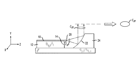
FIGs. 4 -7 illustrate an exemplary embodiment of the present invention. In
particular, FIG. 4 is a side view of an exemplary substrate-based optical
system utilizing
the coupling arrangement of the present invention. The optical system
comprises an
optical waveguide 10 formed along an optical substrate 12 and terminating at
an endface
4
CA 02727931 2010-12-13
WO 2009/155252
PCT/US2009/047427
14 of substrate 12. As with the prior art arrangement described above, the
optical signal
is defined as propagating along the Z-axis of the system, where endface 14
defines the
XY plane of the optical system.
In accordance with the present invention, a first collimation operation is
performed by a two-dimensional lensing surface 20 formed at the termination of
waveguide 10 along endface 14. Two-dimensional lensing surface 20 is
configured, in
this example, to collimate the X-axis wavefront of the propagating optical
beam. For the
purposes of the present invention this collimated signal is designated as Cs.
FIG. 5, an
enlarged isometric view of a portion of endface 14, best illustrates the
location and shape
of an exemplary two-dimensional lensing surface 20. In a preferred embodiment
of a
silicon-based optical system, techniques such as reactive ion etching or
plasma etching
may be used to create the cylindrical profile of lensing surface 20 along
endface 14.
While two-dimensional lensing surface 20 is shown in this example as being
cylindrical in structure, it is to be understood that various other two-
dimensional
geometries may be used, when appropriate. In particular, a grating element or
Fresnel
structure may be used as two-dimensional lensing surface 20. Again, the
preferred
silicon-based optical system embodiment can utilize CMOS processing techniques
to
create a grating, Fresnel structure, or any other appropriate two-dimensional
lensing
surface. In general, any configuration which will provide collimation along
one axis
may be used as a two-dimensional lensing surface in accordance with the
present
invention.
FIG. 6, which is an isometric view of optical substrate 12 and lensing surface
20,
shows the truncated conic geometry of collimated signal Cx. That is, lensing
surface 20
provides collimation along the X-axis and limits the expansion of the beam in
this
particular direction. As shown, the beam exiting two-dimensional lensing
surface 20
will continue to propagate along the Z-axis and will continue to expand in the
Y-axis
direction. FIG. 7 is a top view of the embodiment of FIG. 4, showing in
particular the
relationship between first lensing surface 20 and collimated beam Cx as formed
in
accordance with the present invention.
As described above, the coupling system of the present invention includes a
second two-dimensional lensing surface. Referring to FIG. 4, this second two-
dimensional lensing surface takes the form of a curved surface 22 of a turning
mirror 24.
Turning mirror 24 is disposed along the Z-axis of the optical system and
positioned to
intercept the collimated bean Cx exiting two-dimensional lensing surface 20.
5
CA 02727931 2010-12-13
WO 2009/155252
PCT/US2009/047427
In this example, turning mirror 24 is used to re-direct the X-axis collimated
beam
Cx upwards, providing collimation of propagating collimated beam Cx along the
orthogonal axis (referred to herein as the Y axis), thus forming a signal
which is also
collimated along the Y axis, defined as collimated beam C-y. As will be
described
below, the curvature of second two-dimensional lensing surface 22 may be
configured to
provide, for example, focusing instead of collimation. In one embodiment, for
example,
a parabolic-shaped lensing surface may be used.
In general, the operation performed by second two-dimensional lensing surface
22 may be defined as "beam shaping", where this shaping is considered to
include both
collimation and focusing. Again, the use of silicon-based arrangement as the
preferred
embodiment of the present invention allows for the curvature of surface 22 to
be
controlled through well-known CMOS fabrication processes to provide the
desired type
of beam shaping. Indeed, an integrated monolithic optical system can be
provided where
optical substrate 12 and turning mirror 24 are disposed on and formed within a
common
silicon substrate 15.
The difference between expanding beam 0 of the prior art (FIG. 1) and twice-
collimated beam Cxy of the present invention (FIG. 4) is evident in these
views and is
most particularly demonstrated by comparing the spot size of beam 0 in FIG. 1
and the
spot size of beam C,yy in FIG. 4. The narrowed, concentrated area of beam Cy
ensures
that most of the propagating signal will ultimately be coupled into an
associated optical
signal path, receiver, fiber, etc.
In embodiments where optical substrate 12 and optical waveguide 10 are part of
a
silicon-based optical system, CMOS processing and fabrication techniques can
be used
to form a lensing surface as an integral part of the system, where in the
above-described
embodiment two-dimensional lensing surface 20 is shown as created directly
along
endface 14 as an integral part of substrate 12. The ability to create an
integrated,
monolithic structure allows for the lensing surface to be precisely aligned
with the
optical waveguide without needing to perform any separate alignment and
attachment
processes. Moreover, as will be discussed below, the utilization of a silicon-
based
arrangement and the ability to integrate the lensing surfaces directly into
the structure
allows for an array of structures to be easily formed and reproduced. Indeed,
a preferred
silicon-based optical system comprises an SOI structure, with waveguide(s)
formed in a
surface silicon layer of an SOI structure; the lensing surfaces are likewise
formed of
silicon and integrated within the SOI structure.
6
CA 02727931 2010-12-13
WO 2009/155252
PCT/US2009/047427
FIG. 8 is a top view of a prior art array waveguide and turning mirror
structure,
including a plurality of separate waveguides 1-1, 1-2 and 1-3, all formed
within substrate
2. A single, extended turning mirror surface 4 is used in this case to
intercept the
plurality of optical beams 0-1, 0-2 and 0-3, directing them upwards as shown.
The spot
size of the expanding beams is also illustrated in FIG. 8.
FIG. 9, alternatively, illustrates the use of a plurality of cylindrical (for
example)
lenses 20-1, 20-2 and 20-3 in combination with a plurality of waveguides 10-1,
10-2 and
10-3 to form a plurality of x-axis collimated beams Cx-1, Cx-2 and Cx-3, in
accordance
with the teachings of the present invention. FIG. 10 is an isometric view of
the
arrangement of FIG. 9. Lenses 20-1, 20-2 and 20-3 are individually formed
along
endface 14 of optical substrate 12. Advantageously, CMOS processing may be
used to
ensure that each lens is properly aligned with its associated waveguide, and
that each
lens exhibits the same curvature. Although the arrangement shown in FIGs. 9
and 10
only illustrate a set of three waveguides, it is to be understood that any
desired number of
waveguides and associated lensing surfaces may be formed in alignment thereto.
As best shown in FIG. 10, a single curved surface 22 is preferably used to
separately collimate each beam along the Y axis, while also directing the
plurality of
beams upward. These twice-collimated beams are shown as Cxy-1, Cxy-2 and Cxy-3
in
FIGs. 9 and 10. Advantageously, the formation of an integrated array structure
allows
for alignment to be maintained without the need to separately align each pair
of lensing
surfaces with its associated waveguide.
While the arrangements described above illustrate the use of a first two-
dimension lensing surface to provide X-axis collimation and a curved turning
mirror to
provide Y-axis collimation, it is also possible to reverse these operations.
FIG. 11
illustrates an alternative embodiment of the present invention where a first
lensing
surface 30 is configured to provide Y-axis collimation of a beam exiting at
endface 14 of
waveguide 10 and an associated turning mirror 32 is formed to exhibit a curved
surface
34 (along the X-axis) to provide both X-axis collimation and beam re-
direction. In this
example, the beam is directed downward, perhaps into a photoreceiving device
(not
shown).
FIG. 12 is an isometric view of the waveguide portion of this embodiment,
illustrating the orientation of a two-dimensional lensing surface with respect
to endface
14. As with the embodiments described above, when fabricated as a preferred
silicon-
based configuration, two-dimensional lensing surface 30 may be formed as an
integral
7
CA 02727931 2010-12-13
WO 2009/155252
PCT/US2009/047427
part of substrate 12 along endface 14 at waveguide 10. The ability to form an
integrated
structure eliminates the need to align and affix one component to another. The
use of a
silicon-based embodiment also allows for curved surface 32 to be formed using
known
CMOS processing to provide both the desired degree of X-axis collimation and
re-
direction of the propagating, collimated beam Cyx. It is to be noted that the
subscripts
associated with collimated signal "C" denote the order of the collimation
along the two
axes (i.e., XY or YX).
Moreover, as mentioned above, the degree of curvature in the second lensing
surface may be used to further narrow the impinging beam, so as to focus into
a smaller
spot size than achieved merely by collimating the signal. FIG. 13 shows an
optical
coupling system of the present invention wherein a parabolic curvature is
introduced into
a curved surface 40 of a turning mirror 42, creating a propagating signal with
a focused
spot size F, as shown. While this embodiment shows the use of a parabolic
shape, other
curvatures may be used to provide focusing and/or collimation as desired.
While the above embodiments have been described in terms of a substrate-based
optical system comprising silicon components (which may be readily formed and
aligned
using CMOS processes), it is also possible to form the dual two-dimensional
collimation
and re-direction coupling system of the present invention with discrete
devices. In
general, while the foregoing description represents exemplary embodiments of
the
present invention, it will be obvious to those skilled in the art that various
modifications
may be made without departing from the spirit and scope of the invention as
defined by
the claims appended hereto.
8