Note: Descriptions are shown in the official language in which they were submitted.
CA 02728055 2010-12-14
1
Process for producing electrodes for solar cells
Description
The invention relates to a process for producing electrodes for solar cells,
the electrode
being configured as an electrically conductive layer on a substrate for solar
cells.
Solar cells comprise generally a semiconductor substrate with a number of p-
and
n-doped regions which generate a potential difference and a voltage with one
another
when they are exposed to sunlight. In order to be able to draw off the
voltage,
electrodes are applied to the surfaces of the semiconductor substrate. At
present, the
electrodes are generally applied in a screenprinting process. The production
of
electrodes in a screenprinting process is described, for example, in EP-A 1
911 584,
US-A 2007/0187652 or US 4,375,007.
As an alternative, for example, WO 2008/021782 discloses first applying a
metal layer
to the semiconductor material, applying a covering resist by an inkjet
printing process,
which covers the regions which are to form the structure of the electrodes,
and then
removing the uncovered regions of the metal layer by an etching process.
Subsequently, the covering resist is removed again.
The introduction of contact orifices into a passivation layer on a
semiconductor
substrate, for example by means of laser-based systems, is described in EP-A 1
833
099. After the introduction of the contact orifices, a direct-writing
metalization process
introduces a metal into the contact orifices. Examples of direct-writing
metalization
processes mentioned are inkjet processes or extrusion processes. Finally, a
high-
conductivity material is applied to the contact material deposited beforehand
and
between the contacting orifices.
DE-A 10 2006 033 887 discloses applying an electrically conductive layer to a
substrate, by transferring a transfer layer comprising an electrically
conductive polymer
from a transfer film to the substrate.
One disadvantage of the printing and embossing processes known from the prior
art is
that printing resolution is limited especially in the case of screenprinting,
and conductor
tracks with a width of less than 120 pm cannot be printed. Efficient power
generation in
solar cells, however, requires a maximum usable surface area, which is why it
is
desirable also to print conductor track structures with smaller dimensions.
CA 02728055 2010-12-14
...... ........._..
2
A further disadvantage of the printing and embossing processes is that they do
not
proceed contactiessly and the substrate can fracture owing to the pressure
applied by
the contact, for example with screen and blade in the course of
screenprinting. In
contactless processes, no pressure is exerted on the substrate, and so the
risk of
fracture of the substrate is significantly reduced. The contactless processes
known
from the prior art are generally etching processes, which have the
disadvantage that
acids and alkalis have to be used for the etching and subsequent removal of
the
covering resist. In addition, several complicated process steps are required.
it is an object of the invention to provide a process for producing electrodes
for solar
cells, the electode being configured as a electrically conductive layer, which
enables
the electrically conductive layer also to be reproduced in very fine
structures and which
can be performed in a simple manner with the use of large amounts of
environmentally
hazardous substances.
The object is achieved by a process for producing electrodes for solar cells,
the
electrode being configured as an electrically conductive layer on a substrate
for solar
cells, which comprises the following steps:
a) transferring a dispersion comprising electrically conductive particles from
a carrier
to the substrate by irradiating the dispersion with a laser,
b) drying and/or hardening the dispersion transferred to the substrate to form
the
electrically conductive layer.
Suitable substrates for the solar cell to which the electrically conductive
layer is applied
are, for example, all rigid or flexible substrates which are suitable for
producing solar
cells. Suitable substrates are, for example, monocrystalline, multicrystalline
or
amorphous silicon, Ill-V semiconductors, for example GaAs, GaSb, GaInP,
GaInP/GaAs, GaAs/Ge, or II-VI semiconductors, for example CdTe, or I-Ill-VI
semiconductors, for example CuInS2, CuGaSe2: or those of the general formula
ABC2
where A is copper, silver, gold, B is aluminum, gallium or indium, and C is
sulfur,
selenium or tellurium.
Additionally suitable are all rigid or flexible substrates which are coated
with the
aforementioned semiconductor materials. Such rigid and flexible substrates
are, for
example, glass or polymer films.
In a first step, a dispersion which comprises electrically conductive
particles is
transferred from a carrier to the substrate. The transfer is effected by
irradiation of the
dispersion on the carrier with a laser.
CA 02728055 2010-12-14
3
The electrically conductive layer which is applied to the substrate may cover
the whole
surface or be structured. Transfer of the dispersion with the laser also
allows very fine
structures to be obtained, for example with dimensions of less than 120 pm,
preferably
of less than 100 pm, especially of less than 80 pm. These dimensions relate in
particular to the width of individual tracks.
Before the dispersion with the electrically conductive particles present
therein is
transferred, it is preferably applied to the support over the whole surface.
Alternatively,
it is of course also possible that the dispersion is applied to the carrier in
a structured
manner. However, preference is given to application of the dispersion over the
whole
surface.
Suitable carriers are all materials transparent to the particular laser
radiation, for
example plastic or glass. For example, in the case of use of IR lasers, it is
possible to
use polyolefin films, PET films, polyimide films, polyamide films, PEN films,
polystyrene
films or glass.
The carrier may be either rigid or flexible. In addition, the carrier may be
present as a
tube or continuous film, sleeve or as a flat carrier.
Suitable laser sources for generating the laser beam are commercially
available. It is
possible in principle to use all laser beam sources. Such laser beam sources
are, for
example, pulsed or continuous gas, fiber, solid state, diode or excimer
lasers. These
can be used in each case provided that the particular carrier is transparent
to the laser
radiation, and the dispersion which comprises the electrically conductive
particles and
has been applied to the carrier sufficiently absorbs the laser radiation in
order to
generate a cavitation bubble in the electrically conductive layer as a result
of
conversion of light to thermal energy.
Preference is given to using, as the laser source, pulsed or continuous (cw)
IR lasers,
for example Nd:YAG lasers, Yb:YAG lasers, fiber lasers or diode lasers. These
are
inexpensive and available at high power. Particular preference is given to
continuous
(cw) IR lasers. Depending on the absorption capacity of the dispersion which
comprises the electrically conductive particles, it is, however, also possible
to use
lasers with wavelengths in the visible range or in the UV frequency range.
Suitable
lasers for this purpose are, for example, Ar lasers, HeNe lasers, frequency-
multiplied
IR solid-state lasers or excimer lasers, such as ArF lasers, KrF lasers, XeCl
lasers or
XeF lasers. Depending on the laser beam source, the laser power and the optics
and
modulators used, the focus diameter of the laser beam is in the range between
1 pm
CA 02728055 2010-12-14
4
and 100 l.tm.
The wavelength of the laser beam that the laser generates is preferably within
the
range from 150 to 10 600 nm, especially within the range from 600 to 10 600
nm.
To generate the structure of the electrically conductive layer, it is also
possible to
arrange a mask in the beam path of the laser or to employ an imaging process
known
to those skilled in the art.
In a preferred embodiment, the desired parts of the dispersion which has been
applied
to the carrier and comprises the electrically conductive particles are
transferred to the
substrate by means of a laser focused onto the dispersion.
To perform the process according to the invention, the laser beam and/or the
carrier
and/or the substrate can be moved. The laser beam can, for example, be moved
by
optics known to those skilled in the art with rotating mirrors. The carrier
can, for
example, be configured as a rotating continuous film which is coated
continuously with
the dispersion comprising the electrically conductive particles. The substrate
can be
moved, for example, by means of an XY stage or as a continuous film with
unwinding
and winding device.
The dispersion which is transferred from the carrier to the substrate
generally
comprises electrically conductive particles in a matrix material. The
electrically
conductive particles may be particles of any desired geometry composed of any
desired electrically conductive material, composed of mixtures of different
electrically
conductive materials or else composed of mixtures of electrically conductive
and
nonconductive materials. Suitable electrically conductive materials are, for
example,
carbon such as carbon black, graphite, graphenes or carbon nanotubes,
electrically
conductive metal complexes or metals. Preferably, nickel, copper, silver,
gold,
aluminum, titanium, palladium, platinum, and alloys thereof, or metal mixtures
which
comprise at least one of these metals, are present. Especially preferred are
aluminum,
copper, nickel, silver, titanium, carbon and mixtures thereof.
The electrically conductive particles preferably possess a mean particle
diameter of
from 0.001 to 100 pm, preferably from 0.002 to 50 pm and especially preferably
from
0.005 to 15 pm. The mean particle diameter can be determined by means of laser
diffraction measurement, for example on a Microtrac X100 instrument. The
distribution
of the particle diameters depends on the preparation process thereof.
Typically, the
diameter distribution has only one maximum, though several maxima are also
possible.
In order to achieve particularly tight packing of the particles, preference is
given to
CA 02728055 2010-12-14
using different particle diameters. For example, particles with a mean
particle diameter
of more than 1 pm may be mixed with nanoparticles having a mean particle
diameter of
less than 100 nm.
5 The surface of the electrically conductive particles may be provided at
least partly with
a coating. Suitable coatings may be of inorganic or organic nature. Inorganic
coatings
are, for example, SiO2. It will be appreciated that the electrically
conductive particles
may also be coated with a metal or metal oxide. The metal may likewise be
present in
partly oxidized form.
When two or more different metals are to form the electrically conductive
particles, this
can be done by means of a mixture of these metals. It is especially preferred
when the
metals are selected from the group consisting of aluminum, silver, copper,
nickel,
titanium, platinum and palladium.
However, the electrically conductive particles may also comprise a first metal
and a
second metal, in which case the second metal is present in the form of an
alloy with the
first metal or one or more other metals, or the electrically conductive
particles comprise
two different alloys.
In addition to the selection of the electrically conductive particles, the
shape of the
particles has an influence on the properties of the dispersion after coating.
With regard
to the shape, numerous variants known to those skilled in the art are
possible. The
shape of the electrically conductive particles may, for example, be acicular,
cylindrical,
platelet-shaped or spherical. These particle shapes constitute idealized
shapes, from
which the actual shape, for example as a result of preparation, can deviate to
a greater
or lesser degree. For example, droplet-shaped particles are a real deviation
from the
idealized spherical shape in the context of the present invention.
The electrically conductive particles with various particle shapes are
commercially
available.
When mixtures of electrically conductive particles are used, the individual
mixture
components may also possess different particle shapes and/or particle sizes.
It is also
possible to use mixtures of only one type of electrically conductive particles
with
different particle sizes and/or particle shapes. In the case of different
particle shapes
and/or particle sizes, preference is likewise given to the metals aluminum,
silver,
copper, nickel, titanium, platinum and palladium, and also carbon.
When mixtures of particle shapes are used, preference is given to mixtures of
spherical
CA 02728055 2010-12-14
6
particles with platelet-shaped particles. In one embodiment, for example,
spherical
silver particles are used with platelet-shaped silver particles and/or carbon
particles of
other geometries. In an alternative embodiment, spherical silver particles are
combined
with platelet-shaped aluminum particles.
As already detailed above, the electrically conductive particles can be added
to the
dispersion in the form of their powders. Such powders, for example metal
powders, are
common commercial products and can be produced easily by means of known
processes, for instance by electrolytic deposition or chemical reduction from
solutions
of metal salts or by reduction of an oxidic powder, for example by means of
hydrogen,
by spraying or jetting a metal melt, especially into cooling media, for
example gases or
water. Preference is given to gas and water jetting, and to the reduction of
metal
oxides. Metal powders of the preferred particle size can also be prepared by
grinding
coarser metal powders. A ball mill, for example, is suitable for this purpose.
Platelet-shaped electrically conductive particles can be controlled by
optimized
conditions in the preparation process or be obtained subsequently by
mechanical
treatment, for example by treatment in a stirred ball mill.
Based on the total weight of the dried coating, the proportion of electrically
conductive
particles is in the range from 20 to 98% by weight. A preferred range of the
content of
electrically conductive particles is from 30 to 95% by weight based on the
total weight
of the dried coating.
Suitable matrix materials are, for example, binders with an anchor group
having
pigment affinity, natural and synthetic polymers and derivatives thereof,
natural resins
and synthetic resins and derivatives thereof, natural rubber, synthetic
rubber, proteins,
cellulose derivatives, drying and nondrying oils and the like. These may - but
need not -
be chemically or physically curing, for example air-curing, radiation-curing
or
temperature-curing.
The matrix material is preferably a polymer or polymer mixture.
Polymers preferred as matrix material are ABS (acrylonitrile-butadiene-
styrene); ASA
(acrylonitrile-styrene-acrylate); acrylated acrylates; alkyd resins;
alkylvinyl acetates;
alkylene-vinyl acetate copolymers, in particular methylene-vinyl acetate,
ethylene-vinyl
acetate, butylene-vinyl acetate; alkylene-vinyl chloride copolymers; amino
resins;
aldehyde resins and ketone resins; cellulose and cellulose derivatives, in
particular
hydroxyalkylcellulose, cellulose esters, such as cellulose acetates, cellulose
propionates, cellulose butyrates, carboxyalkylcelluloses, cellulose nitrate;
CA 02728055 2010-12-14
7
ethylcellulose, methylcellulose, epoxy acrylates; epoxy resins; modified epoxy
resins,
e.g. bifunctional or polyfunctional bisphenol A or bisphenol F resins, epoxy-
novolac
resins, brominated epoxy resins, cycloaliphatic epoxy resins; aliphatic epoxy
resins,
glycidic ethers, vinyl ethers, ethylene-acrylic acid copolymers; hydrocarbon
resins;
MABS (transparent ABS comprising acrylate units); melamine resins, maleic
anhydride
copolymers; methacrylates; natural rubber; synthetic rubber; chlorinated
rubber; natural
resins; rosins; shellac, phenolic resins; polyesters; polyester resins, such
as phenyl
ester resins; polysulfones; polyether sulfones; polyamides; polyimides;
polybutylene
terephthalate (PBT); polycarbonate (for example Makrolon from Bayer AG);
polyester
acrylates; polyether acrylates; polyethylene; polyethylene-thiophenes;
polymethyl
methacrylate (PMMA); polyphenylene oxide (PPO); polystyrenes (PS); polyvinyl
compounds, in particular polyvinyl chloride (PVC), PVC copolymers, PVdC,
polyvinyl
acetate, and also their copolymers, if appropriate partially hydrolyzed
polyvinyl alcohol,
polyvinyl acetals, polyvinyl acetates, polyvinylpyrrolidone, polyvinyl ethers,
polyvinyl
acrylates and polyvinyl methacrylates in solution and as dispersion, and also
their
copolymers, polyacrylates and polystyrene copolymers; polystyrene (impact-
modified
or non-impact-modified); polyurethanes, uncrosslinked or crosslinked with
isocyanates;
polyurethane acrylates; styrene-acrylic copolymers; styrene-butadiene block
copolymers (for example Styroflex or Styrolu)e from BASF AG, K-ResihTm from
CPC);
proteins, e.g. casein; SIS triazine resin, bismaleimide-triazine resin (BT),
cyanate ester
resin (CE), allylated polyphenylene ether (APPE). Mixtures of two or more
polymers
can moreover form the matrix material.
Polymers particularly preferred as matrix material are acrylates, acrylate
resins,
cellulose derivatives such as cellulose ethers, e.g. methylcelluloses,
ethylcelluloses, or
cellulose esters, methacrylates, methacrylate resins, melamine and amino
resins,
polyalkylenes, polyimides, epoxy resins, modified epoxy resins, polyvinyl
ethers,
phenolic resins, polyurethanes, polyesters, polyvinyl-acetals, polyvinyl
acetates,
polyvinyl alcohols, polystyrenes, polystyrene copolymers, polystyrene
acrylates,
styrene-butadiene block copolymers, alkylene-vinyl acetates and vinyl chloride
copolymers, polyamides, and also their copolymers.
Based on the total weight of the dry coating, the proportion of the organic
binder
component is from 0.01 to 60% by weight. The proportion is preferably from 0.1
to 45%
by weight, more preferably from 0.5 to 35% by weight.
The dispersion comprising the electrically conductive particles may
additionally
comprise a glass frit. The proportion of glass frit, based on the dry coating,
is preferably
in the range from 0.1 to 15% by weight, preferentially in the range from 0.5
to 10% by
weight and more preferably in the range from 1 to 5% by weight. The glass used
for the
CA 02728055 2010-12-14
8
glass frit has a softening point which is generally within the range from 450
to 550 C.
The glass frit added to the dispersion may comprise alkali metal oxides, for
example
Na20, K20, Li20, alkaline earth metal oxides, for example MgO, CaO, SrO or
BaO, or
further metal oxides, for example B203, Bi203, A1203, Si02, ZnO, TiO2, Zr02,
PbO, AgO
or W03. The oxides may each be present in the glass frit individually or as a
mixture of
two or more oxides. When two or more oxides are present as a mixture in the
glass frit,
any desired mixing ratio of the individual oxides is possible.
In order to be able to apply the dispersion comprising the electrically
conductive
particles and the matrix material to the carrier, a solvent or a solvent
mixture may
additionally be added to the dispersion, in order to establish the viscosity
of the
dispersion which is suitable for the particular application process. Suitable
solvents are,
for example, aliphatic and aromatic hydrocarbons (for example n-octane,
cyclohexane,
toluene, xylene), alcohols (for example methanol, ethanol, 1-propanol, 2-
propanol, 1-
butanol, 2-butanol, amyl alcohol), polyhydric alcohols such as glycerol,
ethylene glycol,
propylene glycol, neopentyl glycol, alkyl esters (for example methyl acetate,
ethyl
acetate, propyl acetate, butyl acetate, isobutyl acetate, isopropyl acetate,
2,2,4-
trimethyl-1,3-pentanediol monoisobutyrate), alkoxy alcohols (for example
methoxypropanol, methoxybutanol, ethoxypropanol), alkylbenzenes (for example
ethylbenzene, isopropylbenzene), butylglycol, butyldiglycol, alkylglycol
acetates (for
example butylglycol acetate, butyldiglycol acetate, propylene glycol methyl
ether
acetate), diacetone alcohol, diglycol dialkyl ethers, diglycol monoalkyl
ethers,
dipropylene glycol dialkyl ethers, dipropylene glycol monoalkyl ethers,
diglycol alkyl
ether acetates, dipropylene glycol alkyl ether acetate, dioxane, dipropylene
glycol and
ethers, diethylene glycol and ethers, DBE (dibasic esters), ethers (for
example diethyl
ether, tetrahydrofuran), ethylene chloride, ethylene glycol, ethylene glycol
acetate,
ethylene glycol dimethyl ester, cresol, lactones (for example butyrolactone),
ketones
(for example acetone, 2-butanone, cyclohexanone, methyl ethyl ketone (MEK),
methyl
isobutyl ketone (MIBK)), dimethylglycol, methylene chloride, methylene glycol,
methylene glycol acetate, methylphenol (ortho-, meta-, para-cresol),
pyrrolidones (for
example N-methyl-2-pyrrolidone), propylene glycol, propylene carbonate, carbon
tetrachloride, toluene, trimethyloipropane (TMP), aromatic hydrocarbons and
mixtures,
aliphatic hydrocarbons and mixtures, alcoholic monoterpenes (for example
terpineol),
water and mixtures of two or more of these solvents.
Preferred solvents are alcohols (for example ethanol, 1-propanol, 2-propanol,
butanol),
alkoxy alcohols (for example methoxypropanol, ethoxypropanol, butylglycol,
dibutylglycol), butyrolactone, diglycol dialkyl ethers, diglycol monoalkyl
ethers,
dipropylene glycol dialkyl ethers, dipropylene glycol monoalkyl ethers, esters
(for
CA 02728055 2010-12-14
9
example ethyl acetate, butyl acetate, butyl glycol acetate, dibutyl glycol
acetate,
diglycol alkyl ether acetates, dipropylene glycol alkyl ether acetates, DBE,
propylene
glycol methyl ether acetate, 2,2,4-trimethyl-1,3-pentanediol monoisobutyrate),
ethers
(for example tetrahydrofuran, dioxane), polyhydric alcohols such as glycerol,
ethylene
glycol, propylene glycol, neopentyl glycol, ketones (for example acetone,
methyl ethyl
ketone, methyl isobutyl ketone, cyclohexanone), hydrocarbons (for example
cyclohexane, ethyl benzene, toluene, xylene), N-methyl-2-pyrrolidone, water
and
mixtures thereof.
In the case of liquid matrix materials, the particular viscosity can
alternatively also be
established via the temperature in the course of application, or via a
combination of
solvent and temperature.
The dispersion may further comprise a dispersant component. This consists of
one or
more dispersants.
In principle, all dispersants which are known to those skilled in the art for
use in
dispersions and are described in the prior art are suitable. Preferred
dispersants are
surfactants or surfactant mixtures, for example anionic, cationic, amphoteric
or nonionic
surfactants. Cationic and anionic surfactants are described, for example, in
"Encyclopedia of Polymer Science and Technology", J. Wiley & Sons (1966),
volume 5,
pages 816 to 818, and in "Emulsion Polymerisation and Emulsion Polymers",
editors:
P. Lovell and M. EI-Asser, Verlag Wiley & Sons (1997), pages 224 to 226.
However, it
is also possible to use, as dispersants, polymers which have anchor groups
with
pigment affinity and are known to those skilled in the art.
The dispersant may, based on the total weight of the dispersion, be used in
the range
from 0.01 to 50% by weight. The proportion is preferably from 0.1 to 25% by
weight,
more preferably from 0.2 to 10% by weight.
In addition, it is possible to use further additives such as thixotropic
agents, for example
silica, silicates, for example aerosols or bentonites, or organic thixotropic
agents and
thickeners, for example polyacrylic acid, polyurethanes, hydrogenated castor
oil, dyes,
fatty acids, fatty acid amides, plasticizers, wetting agents, defoamers,
lubricants,
desiccants, crosslinkers, photoinitiators, complexing agents, waxes, pigments,
conductive polymer particles.
The proportion of the filler and additive component based on the total weight
of the dry
coating is preferably from 0.01 to 50% by weight. Further preference is given
to from
0.1 to 30% by weight, particular preference to from 0.3 to 20% by weight.
CA 02728055 2010-12-14
If the electrically conductive particles in the dispersion on the carrier do
not sufficiently
absorb the energy of the energy source, for example of the laser, absorbents
can be
added to the dispersion. According to the laser beam source used, it may be
necessary
5 to select different absorbents or else mixtures of absorbents which
effectively absorb
the laser radiation. The absorbent is either added to the dispersion or an
additional
separate absorption layer which comprises the absorbent is applied between the
carrier and the dispersion. In the latter case, the energy is absorbed locally
in the
absorption layer and transferred to the dispersion by thermal conduction.
Suitable absorbents for laser radiation have a high absorption in the region
of the laser
wavelength. Especially suitable are absorbents which have a high absorption in
the
near infrared and in the longer-wave VIS region of the electromagnetic
spectrum. Such
absorbents are suitable especially for absorbing the radiation from high-power
solid-
state lasers, for example Nd-YAG lasers, and also from IR diode lasers.
Examples of
suitable absorbents for the laser radiation are dyes which absorb strongly in
the
infrared spectral region, for example phthalocyanines, naphthalocyanines,
cyanines,
quinones, metal complex dyes, such as dithiolenes, or photochromic dyes.
In addition, suitable absorbents are inorganic pigments, especially
intensively colored
inorganic pigments such as chromium oxides, iron oxides, iron oxide hydrates,
or
carbon in the form of, for example, carbon black, graphite, graphenes or
carbon
nanotubes.
Particularly suitable absorbents for laser radiation are finely divided carbon
types and
finely divided lanthanum hexaboride (LaB6).
In general, from 0.005 to 20% by weight of absorbents based on the weight of
the
electrically conductive particles in the dispersion are used. Preference is
given to using
from 0.01 to 15% by weight of absorbents and particular preference to using
from 0.1
to 10% by weight of absorbents, based in each case on the weight of the
electrically
conductive particles in the dispersion.
The amount of the absorbent added is selected by the person skilled in the art
according to the properties of the dispersion layer desired in each case. In
this
connection, the person skilled in the art will also take into account that the
absorbents
added influence not only the speed and efficiency of the transfer of the
dispersion by
means of the laser, but also other properties, for example the adhesion of the
dispersion on the carrier, the hardening or the electroless coatability and/or
electrocoatability of the electrically conductive layer.
CA 02728055 2010-12-14
11
In the case of a separate absorption layer, this consists in the most
favorable case of
the absorbent and a thermally stable, if appropriate crosslinked material,
such that it is
not itself decomposed under the action of the laser light. In order to bring
about
effective conversion of light energy to thermal energy and to achieve poor
thermal
conduction into the electrically conductive layer, the absorption layer should
be applied
very thinly and the absorbent should be present in a very high concentration
without
adversely affecting the layer properties, for example the adhesion to the
carrier.
Suitable concentrations of the absorbent in the absorption layer are from 25
to 95% by
weight, preferably from 50 to 85% by weight.
The energy which is required to transfer a portion of the dispersions
comprising the
electrically conductive particles can, depending on the laser used and/or the
material
from which the carrier has been produced, be applied either on the side coated
with the
dispersion or on the opposite side to the dispersion. If required, it is also
possible to
use a combination of the two process variants.
The transfer of the fractions of the dispersion from the carrier to the
substrate can be
carried out either on one side or two sides. In this case, the transfer may
involve the
two sides being coated with the dispersion successively or else, for example,
simultaneously from both sides by using two laser sources and two carriers
coated with
the dispersion.
In order to increase the productivity, it is possible to use more than one
laser source.
In a preferred embodiment of the process according to the invention, the
transfer of the
dispersion from the carrier to the substrate is preceded by applying the
dispersion to
the carrier. The application is effected, for example, by a coating process
known to
those skilled in the art. Suitable coating processes are, for example,
casting, such as
curtain casting, roller coating, spreading, knifecoating, brushing, spraying,
dipping or
the like. Alternatively, the dispersion comprising the electrically conductive
particles is
printed onto the carrier by any desired printing process. The printing process
by which
the dispersion is printed on is, for example, a roller or arc printing
process, for example
screenprinting, gravure printing, flexographic printing, letterpress printing,
pad printing,
inkjet printing, offset printing or magnetographic printing processes.
However, any
further printing process known to those skilled in the art is also usable.
In a preferred embodiment, the dispersion is not dried and/or hardened
completely on
the carrier, but rather transferred to the substrate in the wet state. This
enables, for
example, the use of a continuous printing unit, in which the dispersion on the
carrier
CA 02728055 2010-12-14
12
can be renewed constantly. This process regime allows a very high productivity
to be
achieved. Printing units which can be replenished continuously with ink are
known to
those skilled in the art, for example from DE-A 37 02 643. In order to prevent
particles
from sedimenting out of the dispersion, it is preferred when the dispersion is
stirred
and/or pumped in circulation in a reservoir vessel before being applied to the
carrier. In
addition, it is preferred for establishment of the viscosity of the dispersion
when the
temperature of the reservoir vessel in which the dispersion is present can be
controlled.
In a preferred embodiment, the carrier is configured as a continuous belt
which is
transparent for the particular laser radiation, which is moved, for example,
with internal
transport rollers. Alternatively, it is possible to design the carrier as a
cylinder, the
cylinder being movable by means of internal transport rollers or being driven
directly.
The carrier is then coated with the dispersion comprising the electrically
conductive
particles, for example, by a process known to those skilled in the art, for
example with a
roller or a roller system from a reservoir vessel in which the dispersion is
present.
Rotation of the roller or of the roller system takes up the dispersion which
is applied to
the carrier. Movement of the carrier past the coating roller applies a full-
area dispersion
layer to the carrier. In order to transfer the dispersion to the substrate,
the laser beam
source is arranged in the interior of the continuous belt or of the cylinder.
To transfer
the dispersion, the laser beam is focused onto the dispersion layer and,
through the
carrier which is transparent thereto, hits the dispersion and transfers the
dispersion to
the substrate at the site at which it hits the dispersion. Such a printing
unit is described,
for example, in DE-A 37 02 643. The dispersion is transferred, for example, by
virtue of
the energy of the laser beam at least partly evaporating the dispersion and by
virtue of
the gas bubble which forms transferring the dispersion. The dispersion which
is not
transferred from the carrier to the substrate can be reused in a next coating
step.
The layer thickness of the electrically conductive layer which is transferred
to the
substrate by means of the transfer by virtue of the laser varies preferably
within the
range between 0.01 and 50 pm, further preferably between 0.05 and 30 pm and
especially between 0.1 and 20 pm. The electrically conductive layer may be
applied
either over the whole surface or in a structured manner.
Structured application of the dispersion to the carrier is advantageous when
particular
structures are to be produced in high numbers and the structured application
reduces
the amount of dispersion which has to be applied to the carrier. This allows
less
expensive production to be achieved.
In order to obtain a mechanically stable, structured or fully electrically
conductive layer
on the substrate, it is preferred that the dispersion with which the
structured or fully
CA 02728055 2010-12-14
13
electrically conductive layer is applied to the substrate is dried physically
or hardened
after the application. Depending on the matrix material, the drying or the
curing is
effected, for example, by the action of heat, light (UVNis) and/or radiation,
for example
infrared radiation, electron beams, gamma radiation, x-radiation, microwaves.
To
induce the hardening reaction, it may be necessary to add a suitable
activator. The
hardening can also be achieved by combining various processes, for example by
combining UV radiation and heat. The combination of the hardening processes
can be
performed simultaneously or successively. For example, UV or IR radiation can
initially
be used merely to partially harden or partially dry the layer, such that the
structures
formed no longer flow away. Thereafter, the layer can be hardened or dried
further by
the action of heat.
When the substrate is heat-resistant, especially when the substrate does not
comprise
any polymer film, it is preferred to fire the substrate with the electrically
conductive
layer applied thereto, after the drying and/or hardening of the dispersion
transferred to
the substrate, to form the electrically conductive layer, in order to obtain a
completely
electrically conductive surface on the substrate and to establish contact with
the active
semiconductor layer of the substrate.
For the firing, the substrate with the electrically conductive layer applied
thereto is
brought to a temperature in the range from 600 to 900 C in a gradient oven
with a
temperature profile adjusted to the particular formulation and the substrate
for a period
of generally from 30 s to 20 min. As a result, a portion of the metal of the
electrically
conductive layer begins to diffuse into the semiconductor material. The
penetration
depth of the metal into the substrate is adjusted through the temperature and
the
duration. The diffusion of the metal into the substrate gives rise to a solid
bond of
substrate and electrically conductive layer.
For the firing, an infrared furnace is typically used. However, it is also
possible to use
any other suitable furnace with which the temperatures needed for the firing
can be
established. It is also possible to use continuous furnaces, for example as
tunnel
furnaces, or batchwise furnaces.
In one embodiment of the invention, at least one metal layer is deposited on
the
structured or fully electrically conductive layer by electroless coating
and/or
electrocoating.
When the substrate is fired with the electrically conductive layer applied
thereto, the
electroless deposition and/or electrodeposition of the metal layer can be
effected either
before the firing or after the firing.
CA 02728055 2010-12-14
14
The coating can be effected by any process known to those skilled in the art.
The
composition of the electrolyte solution which is used for the coating depends
on what
metal is to be used to coat the electrically conductive layer on the
substrate. Customary
metals which are deposited by electroless coating and/or electrocoating on the
electrically conductive layer are, for example, silver, gold, nickel,
palladium, platinum or
copper. The layer thicknesses of the one or more deposited layers are within
customary ranges known to those skilled in the art.
Suitable electrolyte solutions which can be used to coat electrically
conductive
structures are known to those skilled in the art.
When the electrically conductive particles consist of materials which are
oxidized
easily, it may additionally be necessary to at least partly remove the oxide
layer
beforehand. According to the procedure in the process, for example in the case
of use
of acidic electrolyte solutions, the removal of the oxide layer may take place
simultaneously with the metalization as it sets in, without an additional
process step
being required.
When the electrically conductive particles comprise a material which can
oxidize easily,
in a preferred process variant, the formation of the metal layer on the
structured or fully
electrically conductive layer is preceded by at least partial removal of the
oxide layer.
The oxide layer can be removed, for example, with acids, such as concentrated
or
dilute sulfuric acid or concentrated or dilute hydrochloric acid, nitric acid,
citric acid,
phosphoric acid, amidosulfonic acid, formic acid or acetic acid.
After the electrocoating, the substrate can be processed further by all steps
known to
those skilled in the art. For example, electrolyte residues present can be
removed from
the substrate by rinsing and/or the substrate can be dried.
In an alternative embodiment, at least one metal layer is first deposited onto
the dried
and/or hardened electrically conductive layer by electroless coating and/or
electrocoating, and then the composite comprising the substrate with
electrically
conductive layer formed thereon, on which a further metal layer has been
deposited, is
fired.
The process according to the invention for producing electrically conductive
layers on a
substrate can be operated in continuous, semicontinuous or batchwise mode. It
is also
possible that only individual steps of the process are performed continuously,
while
other steps are performed batchwise.
CA 02728055 2010-12-14
In addition to the production of an electrically conductive layer, it is also
possible by the
process according to the invention to successively apply a plurality of layers
to the
substrate. For example, the performance of the process for producing the first
5 conductive layer may be followed by a printing process as described above to
apply at
least one further structured or fully electrically conductive layer. The at
least one further
electrically conductive layer may, for example, comprise a different
composition of
electrically conductive particles. It is possible here, for example, that the
proportion of
electrically conductive particles in the dispersion is greater, that
electrically conductive
10 particles of another material or electrically conductive particles of the
same materials
but in another mixing ratio or with another particle geometry, are used for
the further
electrically conductive layer.
After generating an electrically conductive layer on one side of the
substrate, it is
15 possible to apply the dispersion either on the topside or on the bottomside
of the
substrate to form the electrically conductive layer. In this case,
electrically conductive
layers both for frontside contact connection and for backside contact
connection of
solar cells are obtained.
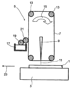
One embodiment of the invention is shown in the sole drawing and is explained
in
detail in the description which follows.
The sole figure shows a schematic of an apparatus for performing the process
according to the invention.
To produce electrodes for solar cells, a substrate 1 is supplied to a coating
device 5
with a transport device 3 which is shown here only schematically. Suitable
transport
devices 3 are any desired transport devices known to those skilled in the art.
For
example, the transport device 3 may comprise a belt on which the substrate 1
is
positioned and which is conducted around rollers in order to move the
substrate 1.
Alternatively, for example, it is possible to use feeders with which the
substrate 1 is
positioned in the coating device 5. It is also possible to use any other
suitable transport
device known to those skilled in the art.
The coating device 5 comprises a carrier 7 which is coated with a dispersion.
In order
to coat the substrate 1, the carrier 7 coated with the dispersion is
irradiated with a
laser 9. This detaches the dispersion from the carrier 7 and transfers it to
the
substrate 1. This is done, for example, by evaporating a small amount of the
solvent
which is present in the dispersion, and the generation of a shockwave in the
dispersion,
which subsequently generates a droplet which is detached from the carrier.
CA 02728055 2010-12-14
16
The dispersion applied to the substrate 1 comprises electrically conductive
particles. In
this way, an electrically conductive layer is obtained on the substrate 1. As
well as the
electrically conductive particles, it is also possible for binders present to
be transferred
from the dispersion to the substrate 1. A layer forms on the substrate 1,
which
comprises both particles and binders. The dispersion is transferred from the
carrier 7 to
the substrate 1, for example, in the form of droplets 11.
A structured coating can be obtained on the substrate 1 by, for example, using
a mask.
It is preferably also possible to achieve the structuring by shifting the
laser, in which
case the laser is simultaneously switched on and off depending on the
structure. This
can be done, for example, by means of an acousto-optical modulator or pulsing
of the
laser. Depending on the diameter of the laser beam which hits the carrier 7,
it is also
possible to obtain very fine structures with dimensions of less than 120 m.
The layer
thickness is preferably in the range between 0.01 and 50 m.
In the embodiment shown in Figure 1, the carrier 7 is conducted by means of
internal
rollers 13. The motion of the carrier 7 is shown by an arrow 15.
Since the dispersion is no longer applied over the full surface of the carrier
7 after the
application of the coating to the substrate 1, it is necessary to coat the
carrier 7 with the
dispersion again after the application of the coating to the substrate 1. For
this purpose,
a reservoir vessel 17 which comprises the dispersion is provided. In the
embodiment
shown here, a roller 19 is immersed into the reservoir vessel 17. An
application
roller 21 is used to apply the dispersion to the carrier 7. In order to remove
the unused
dispersion on the carrier when recoating, it is necessary that the application
roller 21
moves counter to the carrier 7. The application roller 21 may, for example,
have a
structure such that the dispersion is applied to the carrier 7 in structured
form. In this
case, there is likewise structured application to the substrate 1. In general,
the
dispersion is, however, applied over the full surface to the carrier 7.
Alternatively to the embodiment shown here, in which the dispersion is applied
to the
carrier 7 with the aid of a roller application process, it is also possible to
use any
desired other application process, for example screenprinting, gravure
printing, inkjet
printing or flexographic printing.
After the transfer of the dispersion to the substrate 1 with the aid of the
laser 9, the
coating thus obtained is dried or hardened. After the hardening, it is
possible to
metalize the coating on the substrate 1 electrolessly or by electrocoating.
The further
process steps are carried out in apparatuses suitable for this purpose. To
this end, the
CA 02728055 2010-12-14
17
substrate 1, for example, is moved into a further treatment unit by the
transport
device 3. This is shown by an arrow 23.
List of reference numerals
1 Substrate
3 Transport device
5 Coating device
7 Carrier
9 Laser
11 Droplets
13 Roller
15 Movement of the carrier
17 Reservoir vessel
19 Roller
21 Application roller
23 Transport of the substrate