Note: Descriptions are shown in the official language in which they were submitted.
CA 02728410 2013-10-09
=
CAPACITIVE TOUCHPAD AND TOY INCORPORATING THE SAME
CROSS REFERENCE TO RELATED APPLICATIONS
FIELD OF THE DISCLOSURE
[0001] The present disclosure relates to capacitive touchpad
assemblies, as
well as computer peripheral devices resembling toys and having components such
as input capacitive touchpad assemblies and integral card readers. The
touchpads
may use capacitive sensors, and haptic feedback may be provided with a
piezoelectric device. In some embodiments, limited gesture recognition may be
used
to improve play value.
[0002] Examples of capacitive sensors are disclosed in United
States Patent
Nos. US4039940, US4272916, US4355300, US4595913, US5413518, US5650597,
US6661239, US6834251, US6940291 and Publication No. US20040219501.
Examples of piezoelectric devices are disclosed in United States Patent Nos.
US4334280, US6429846 and US6466036. Examples of gesture recognition are
disclosed in United States Patent Publication Nos. US20060205502,
US20060089197, and US20060252494. Examples of card readers are disclosed in
United States Patent Nos. US4884974, US5334022, US7224934, US7387560.
Page 1 of 20¨ PCT APPLICATION Our Ref. MAT3Z126PCT
CA 02728410 2010-12-17
WO 2009/154900 PCT/US2009/043620
SUMMARY
[0004] Capacitive touchpad assemblies, toys including capacitive touchpad
assemblies and, in some cases, integral card readers, and methods for
detecting
contact with a capacitive touch surface are provided. A capacitive touch
surface's
capacitance may vary depending on whether an object such as a human finger is
in
contact with the surface. A voltage of the capacitive touch surface may be
altered
during each of a predetermined number of recurring intervals. The capacitance
of the
capacitive touch surface will determine the amount of time required to alter
its
voltage to a threshold voltage within each interval. The sum amount of time
required
for the voltage of the capacitive touch surface to reach the threshold voltage
in a
predetermined number of intervals may be used to determine whether the
capacitive
touch surface is being touched during that predetermined number of intervals.
BRIEF DESCRIPTION OF THE DRAWINGS
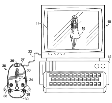
[0005] Fig. 1 depicts a toy according to the present disclosure attached
to a
computer, according to one embodiment of the disclosure.
[0006] Fig. 2 is a front view of a toy including a capacitive touchpad
assembly
with a plurality of capacitive touch surfaces, according to one embodiment of
the
disclosure.
[0007] Fig. 3 depicts an example logic circuit for implementing one or
more of
the embodiments disclosed herein.
[0008] Fig. 4 is a front view of a toy similar to that shown in Fig. 2
with a
playing card overlaying the plurality of capacitive touch surfaces, according
to one
embodiment of the disclosure.
2
CA 02728410 2010-12-17
WO 2009/154900 PCT/US2009/043620
[0009] Fig. 5 is a side view of a toy similar to those shown in Figs. 1-
4,
according to one embodiment of the disclosure.
[0010] Figs. 6 and 7 are front and rear views, respectively, of an
example
playing card usable with devices such as those shown in Figs. 1-5, according
to one
embodiment of the disclosure.
[0011] Fig. 8 depicts example circuit logic for detecting whether a
capacitive
touch surface is being touched, according to one embodiment of the disclosure.
[0012] Fig. 9 depicts two charts showing the differences in capacitance
as a
function of time between a capacitive touch surface being touched and not
being
touched, in a capacitive touchpad assembly incorporating the circuit logic of
Fig. 8.
[0013] Fig. 10 depicts alternative circuit logic for detecting whether a
capacitive touch surface is being touched, according to one embodiment of the
disclosure.
[0014] Fig. 11 depicts two charts showing the differences in capacitance
as a
function of time between a capacitive touch surface being touched and not
being
touched, in a capacitive touchpad assembly incorporating the circuit logic of
Fig. 10.
DETAILED DESCRIPTION
[0015] Referring to the attached drawings, wherein like numerals indicate
like
elements, there is shown in Fig. 1 a computing device 10 including a keyboard
12
and a monitor 14 displaying an image 16. Computing device 10 also may include
any
number of other components that are not shown, such as a mouse, a printer, and
the
like. A peripheral toy 20 may be operably coupled to computing device 10 via
an
interface 22. Interface 22 may be a wired (e.g., USB or Serial) or wireless
(e.g.,
BlueTooth, RFID, Infrared) connection.
3
CA 02728410 2010-12-17
WO 2009/154900 PCT/US2009/043620
[0016] As seen in Fig. 2, peripheral toy 20 may include a housing 24 with
an
integral card reader 26 and a surface 28 adapted to receive one or more
portable
playing cards 30 (see Figs. 1, 3 and 5-6). Fig. 3 depicts an example logic
circuit that
may be implemented in peripheral toys 20 such as those shown in Figs. 1 and 2.
Integral card reader 26 is shown here as a series of optical pickups.
Peripheral toy
20 may also include a CPU 29, also referred to as a controller, which may be
configured to control the interaction of various components of peripheral toy
20.
Additional components will be described further below.
[0017] As shown in Fig. 4, a user may install one or more portable
playing
cards 30 onto surface 28 of peripheral toy 20. Integral card reader 26 may
read
indicia 32 on a surface of playing card 30 (e.g., on the back of playing card
30, as
seen in Fig. 6) to obtain identification information about playing card 30.
CPU 29 may
be configured to receive from integral card reader 26 the playing card
identification
information and to communicate instructions through interface 22 to computing
device 10 to provide an output related to the received identification
information.
[0018] In some embodiments, identification information about playing card
30
may include information relating to a character 34 depicted on card 30.
Placing
playing card 30 on surface 28 may cause CPU 29 to instruct computing device 10
to
output image 16 (see Fig. 1) appearing similar or being related to the
character 34
on computer monitor 14. A user may control image 16 on monitor 14 with
peripheral
toy 20 by manipulating controls on peripheral toy 20 to cause CPU 29 to send
control
signals to computing device 10 via interface 22.
[0019] While many methods of reading data from playing card 30 may be
implemented (e.g., USB, serial, memory card, barcode, RFID), in an exemplary
embodiment, each sensor of integral card reader 26 is configured to optically
read a
4
CA 02728410 2013-10-09
,
single portion of indicia 32 on card 30 to ascertain information about card
30. For
example, the example integral card reader 26 shown in Figs. 2 and 3 includes
five
sensors representing five binary digits, allowing for 31 permutations or
discrete card
identities. While the least significant bit in Fig. 2 is shown on the right,
this is not
intended to be limiting, and it should be understood that the sensors in
integral card
reader 26 may be in any order.
[0019] Figs. 6 and 7 depict the front and back, respectively, of an
example
playing card 30 compatible with the toy 20 shown in Figs. 1-5. lndicia 32 are
seen in
Fig. 7 on the back of card 30 comprising five individual value indicators.
Each value
indicator may be adapted to be read by a single sensor of integral card reader
26.
Each value indicator may be capable of communicating one or more pieces of
information. In this example, the most significant bit of indicia 32 is
arranged
oppositely relative to the most significant bit of the integral card reader 26
so that the
most significant bits will line up when the back of card 30 is faced towards
integral
card reader 26.
[0020] As seen in Figs. 2 and 3, peripheral toy 20 may include
additional
features, such as a camera 36, camera control buttons 37, other input controls
38,
and a four-way directional pad 39. In some embodiments, camera 36 includes an
image sensor and lens, allowing photographs to be taken. Alternatively, camera
36
may be a simulation only, but camera control buttons 37 may be used to trigger
the
display of simulated photographs on computing device 10. Four-way directional
pad
39 may be similar to that described in US4687200.
[0021] Referring back to Fig. 2, peripheral toy 20 may include
controls such as
a capacitive touchpad assembly 40 comprising one or more capacitive
Page 5 of 20¨ PCT APPLICATION Our Ref. MAT3Z126PCT
CA 02728410 2010-12-17
WO 2009/154900 PCT/US2009/043620
touchpads/touch surfaces 42 disposed on housing 24 of peripheral toy 20, often
on
surface 28. In some embodiments, each capacitive touch surface 42 is covered
by a
decorative dielectric material. Contacting a capacitive touch surface 42 with
an
object such as a human finger modifies the effective capacitance of the
capacitive
touch surface 42. This modification of capacitance, and hence whether a
capacitive
touch surface 42 is being touched, may be detected by altering a voltage of
the
capacitive touch surface 42 and measuring the amount of time required for the
capacitive touch surface 42 to reach a threshold voltage.
[0023] Playing card 30 may be constructed of materials chosen so that
placement of card 30 on surface 28 will not interfere with the operation of
capacitive
touchpad assembly 40. For example, capacitive touch surface 42 may be
configured
to detect touching through playing card 30.
[0024] Card 30 also may be usable to improve the usability of capacitive
touchpad assembly 40. For example, card 30 may include one or more control
area
indicators 35 that indicate a particular portion of card 30 that will overlay
a particular
capacitive touch surface 42. The underlying capacitive touch surface 42 may
cause
computing device 10 to alter output image 16 in a manner that is related to
what is
depicted in the particular control area indicator 35. For example, in Fig. 6,
card 30
includes control area indicator 35 depicting clothing. When card 30 is
installed on toy
20, CPU 29 may be configured to alter the clothing of character output 16 when
the
capacitive touch surface 42 underlying this control area indicator 35 is
touched.
[0025] Fig. 8 illustrates example circuit logic for monitoring the
capacitance of
capacitive touch surface 42, and hence whether capacitive touch surface 42 is
being
touched Repeatedly, capacitive touch surface 42 is charged at least until its
voltage
reaches a predetermined threshold value, and the time required to reach the
6
CA 02728410 2010-12-17
WO 2009/154900 PCT/US2009/043620
predetermined charge threshold in each instance is measured. Capacitive touch
surface 42 is connected to a power source Vcc. A pulse generator or clock 44
generates pulses, and in many cases timing pulses, to a logic-controlled
switch 46 to
define recurring intervals. The pulses are also provided to a timer 48. Logic-
controlled switch 46 may be a microchip, an ASIC or other similar circuitry,
and may
be configured to open and close a connection between capacitive touch surface
42
and ground 50 to alter a voltage of capacitive touch surface 42.
[0026] Connection to ground 50 discharges capacitive touch surface 42
quickly, particularly where little to no resistance exists between capacitive
touch
surface 42 and ground 50. However, as will be seen in other embodiments
described
below, a resistor may be included between capacitive touch surface 42 and
ground
50 to cause the discharge of capacitive touch surface 42 to be more gradual.
[0027] A peak level detector 52 is coupled to capacitive touch surface 42
and
is configured to detect, and indicate to timer 48, when the voltage of
capacitive touch
surface 42 reaches the threshold voltage (indicated by dotted line A in Fig.
9).
Accordingly, timer 48 may be configured to capture or measure the time
required to
charge capacitive touch surface 42 to the threshold voltage. Timer 48 may be
started
based on output from pulse generator 44 (e.g., at the beginning of each
interval T,
which typically would be a time interval) and stopped at the instruction of
peak level
detector 52 (i.e., when the threshold voltage is reached). When timer 48
stops, it
may store the measured time in a register 54, and the measured time may be
added
to a sum of captured times contained in an accumulator 56.
[0028] Timer 48 may measure times during a predetermined number of
intervals, or in other words, during a sample. A cycle counter 58 may track
intervals
in order to control sample size. For example, if a sample size is to be X
intervals T,
7
CA 02728410 2010-12-17
WO 2009/154900 PCT/US2009/043620
cycle counter 58 increments X times, during which time accumulator 56
accumulates
X measured charge times from timer 48. Once X cycles pass, the sample is
complete.
[0029] Once a sample is complete, the sum value in accumulator 56 may be
stored and accumulator 56 may be reset to zero. Using control circuitry
implementing
logic indicated generally at 59, the sum value from accumulator 56 then may be
compared to a predetermined value or threshold Y. If it is above (or in some
cases,
greater than or equal to) the threshold Y, then it may be determined in Path A
that
capacitive touch surface 42 was being touched during the sample. If the stored
accumulator value is below the threshold Y, then it may be determined in Path
B that
capacitive touch surface 42 was not being touched during the sample.
[0030] Example results of the circuit logic shown in Fig. 8 are depicted
graphically in Fig. 9. A sample where capacitive touch surface 42 is being
touched is
shown in the top graph labeled "TOUCH." Because capacitive touch surface 42 is
being touched, its capacitance is higher. Accordingly, more of an interval,
e.g., 2/3 of
an interval T, may be required to charge capacitive touch surface 42 to the
threshold
voltage indicated by dotted line A.
[0031] An example where capacitive touch surface 42 is not being touched
is
shown in the bottom graph of Fig. 9 labeled "NO TOUCH." Because the
capacitance
of capacitive touch surface 42 is lower when it is not being touched, less of
an
interval, e.g., only 1/3 of an interval T, may be required to charge
capacitive touch
surface 42 to the threshold voltage indicated by dotted line A.
[0032] Continuing with the logic of Fig. 8 and referring also to Fig. 9,
for each
interval T, 2/3 is added to accumulator 56 when the capacitive touch surface
42 is
being touched and 1/3 is added to accumulator 56 when the capacitive touch
surface
8
CA 02728410 2010-12-17
WO 2009/154900 PCT/US2009/043620
42 is not being touched. Assuming a sample size of 9 intervals T (only 7
intervals are
shown in Fig. 9), if the total sum in accumulator 56 is greater than or equal
a
predetermined value (e.g., 6), then capacitive touch surface 42 may be
considered to
be touched for that sample. In such a case, control circuitry implementing the
logic
indicated generally at 59, which may include one or more of the components
described herein, may produce a signal indicative of the capacitive touch
surface 42
being touched. Likewise, if the total sum in accumulator 56 is less than a
predetermined value (e.g., less than 6), then capacitive touch surface 42 may
be
considered untouched for that sample, and the control circuitry may produce a
signal
indicative of such.
[0033] At the end of each interval T and/or the beginning of the next
interval
T+1, the charging of capacitive touch surface 42 may cease and capacitive
touch
surface 42 may be connected to ground 50 to discharge its voltage, immediately
prior to its being charged again. This creates a break in time between the
charges of
capacitive touch surface 42 that makes a sample readily observable using an
oscilloscope. This also makes the determination of whether capacitive touch
surface
42 is being touched entirely independent of any frequency of a signal, as the
recurring intervals from clock 44 assure a constant frequency.
[0034] Alternative circuit logic is depicted in Fig. 10. This embodiment
is
similar to the one shown in Fig. 8 except that instead of measuring the time
required
to charge capacitive touch surface 42 to a threshold voltage, this embodiment
measures the time required to discharge capacitive touch surface 42 to a
threshold
voltage.
[0035] At the beginning of each interval T and immediately prior to
capacitive
touch surface 42 being discharged, timer 48 is set to zero and logic-
controlled switch
9
CA 02728410 2010-12-17
WO 2009/154900 PCT/US2009/043620
46 connects capacitive touch surface 42 to a power supply Vcc for either a
predetermined amount of time or until a predetermined charge (labeled B in
Fig. 11)
is reached. Once capacitive touch surface 42 is charged, logic-controlled
switch 46
disconnects capacitive touch surface 42 from the power supply Vcc so that the
voltage of capacitive touch plate 42 is gradually discharged through a
discharge
resistor.
[0036] In Fig. 10, a zero level detector 60 is connected to capacitive
touch
surface 42 to detect when the voltage of the capacitive touch surface 42 drops
to
zero. Once this happens, zero level detector 60 instructs timer 48 to stop.
Accordingly, the time measured by timer 48 is the time required to charge
capacitive
touch surface 42, plus the time required to discharge the voltage of
capacitive touch
surface 42 to zero. As was the case above, the sum of the measured times for a
sample are accumulated in accumulator 56. The remaining logic may be identical
to
that shown in Fig. 8. Although a zero level detector 60 is shown in Fig. 10,
indicating
a predetermined threshold value of zero, it should be understood that other
non-zero
predetermined threshold values may also be selected.
[0037] Example results of the logic circuit shown in Fig. 10 are depicted
graphically in Fig. 11. A sample where a capacitive touch surface 42 is being
touched is shown in the top graph of Fig. 11 labeled "TOUCH." Because
capacitive
touch surface 42 is being touched, its capacitance is higher, which means more
time
is required for it to discharge. In this case, 1/2 of an interval T is
required to
discharge capacitive touch surface 42 to zero. In the bottom graph of Fig. 11
labeled
"NO TOUCH", capacitive touch surface 42 is not being touched, making its
capacitance lower and decreasing the time required for it to discharge. In
this case,
1/4 of an interval T is required to discharge capacitive touch surface 42 to
zero.
CA 02728410 2010-12-17
WO 2009/154900 PCT/US2009/043620
[0038] Assuming a sample size of 5 intervals T, the amount of time
accumulated in accumulator 56 may be compared to a threshold of Y=2.5. If the
accumulated time is greater than or equal to 2.5 (1/2 x 5 = 2.5), then it may
be
determined that capacitive touch surface 42 is being touched. In such a case,
the
control circuitry implementing the logic indicated at 59 may produce a signal
indicative of the capacitive touch surface 42 being touched. If the
accumulated time
is less than 2.5 (1/4 x 5 = 1.25), then it may be determined that the
capacitive touch
surface 42 is not being touched, and the control circuitry may produce a
signal
indicating as much. It should be understood that the threshold to which the
accumulated time is compared may be adjusted upwards or downwards, decreasing
or increasing, respectively, the sensitivity of capacitive touch surface 42.
[0039] In some embodiments, a signal communicated from peripheral toy 20
to computing device 10 via interface 22 may utilize one or more communication
or
electronic protocols. For example, actions taken using capacitive touchpad
assembly
40 or other controls on peripheral toy 20 may be transmitted to computing
device 10
in a format such as USB. In some embodiments, software executing on computing
device 10 may be operated even without toy 20 (where toy 20 is lost or
damaged)
using another USB input device. The following list contains an example set of
USB
keystrokes that may be mapped to various capacitive touch pads on toy 20.
Up = Alt_Up Arrow = E2h OR E6h AND 52h Usage ID
Dn = Alt_Down Arrow = E2h OR E6h AND 51h Usage ID
Rt = Alt Right Arrow = E2h OR E6h AND 4Fh Usage ID
Lt = Alt_Left Arrow = E2h OR E6h AND 50h Usage ID
Camera = Alt_Spacebar = E2h OR E6h AND 2Ch Usage ID
Yes = Alt_Enter = E2h OR E6h AND 28h Usage ID
No = Alt_Backspace = E2h OR E6h AND 2Ah Usage ID
Sw01 = Alt_Q = E2h OR E6h AND 14h Usage ID
Sw02 = Alt _W = E2h OR E6h AND 1Ah Usage ID
Sw03 = Alt _E = E2h OR E6h AND 08h Usage ID
Sw04 = Alt _R = E2h OR E6h AND 15h Usage ID
Sw05 = Alt _T = E2h OR E6h AND 17h Usage ID
11
CA 02728410 2010-12-17
WO 2009/154900 PCT/US2009/043620
Sw06 = AILY = E2h OR E6h AND 1Ch Usage ID
Sw07 = Alt _A = E2h OR E6h AND 04h Usage ID
Sw08 = Alt _S = E2h OR E6h AND 16h Usage ID
5w09 = Alt _D = E2h OR E6h AND 07h Usage ID
Sw10 = Alt _F = E2h OR E6h AND 09h Usage ID
Sw11 = Alt _G = E2h OR E6h AND 0Ah Usage ID
5w12 = Alt _Z = E2h OR E6h AND 1Dh Usage ID
Card01 = Alt 1 = E2h OR E6h AND lEh Usage ID
Card02 = Alt _2 = E2h OR E6h AND 1Fh Usage ID
Card03 = Alt_3 = E2h OR E6h AND 20h Usage ID
Card04 = Alt_4 = E2h OR E6h AND 21h Usage ID
Card05 = Alt_5 = E2h OR E6h AND 22h Usage ID
Card06 = Alt_6 = E2h OR E6h AND 23h Usage ID
Card07 = Alt_7 = E2h OR E6h AND 24h Usage ID
Card08 = Alt_8 = E2h OR E6h AND 25h Usage ID
Card09 = Alt_9 = E2h OR E6h AND 26h Usage ID
Card10 = AIL() = E2h OR E6h AND 27h Usage ID
Card11 = Alt _U = E2h OR E6h AND 18h Usage ID
Card12 = Alt _P = E2h OR E6h AND 13h Usage ID
Card13 = Alt_H = E2h OR E6h AND OBh Usage ID
Card14 = Alt_J = E2h OR E6h AND ODh Usage ID
Card15 = AILK = E2h OR E6h AND OEh Usage ID
Card16 = AILL = E2h OR E6h AND OFh Usage ID
Card17 = Alt_N = E2h OR E6h AND 11h Usage ID
Card18 = Alt_M = E2h OR E6h AND 10h Usage ID
Card19 = Alt_< = E2h OR E6h AND 36h Usage ID
Card20 = Alt_> = E2h OR E6h AND 37h Usage ID
[0040] While embodiments of a toy and associated computer systems and
methods of use have been particularly shown and described, many variations may
be made therein. This disclosure may include one or more independent or
interdependent embodiments directed to various combinations of features,
functions,
elements and/or properties. Other combinations and sub-combinations of
features,
functions, elements and/or properties may be claimed later in this or a
related
application. Such variations, whether they are directed to different
combinations or
directed to the same combinations, whether different, broader, narrower or
equal in
scope, are also regarded as included within the subject matter of the present
disclosure. Accordingly, the foregoing embodiments are illustrative, and no
single
feature or element, or combination thereof, is essential to all possible
combinations
12
CA 02728410 2010-12-17
WO 2009/154900 PCT/US2009/043620
that may be claimed in this or a later application. Where the description
recites "a" or
"a first" element or the equivalent thereof, such description includes one or
more
such elements, neither requiring nor excluding two or more such elements.
Further,
ordinal indicators, such as first, second or third, for identified elements
are used to
distinguish between the elements, and do not indicate a required or limited
number
of such elements, and do not indicate a particular position or order of such
elements
unless otherwise specifically stated.
13