Note: Descriptions are shown in the official language in which they were submitted.
CA 02729233 2010-12-23
WO 2009/158330 PCT/US2009/048236
BALLAST WITH LAMP FILAMENT DETECTION
Cross-Reference to Related 212lication
[0001] This application claims benefit of United States Provisional
Application Number
61/076,039, filed June 26, 2008, which is hereby incorporated herein by
reference in its entirety.
Field of the Invention
[0002] The present invention relates to the general subject of circuits for
powering gas
discharge lamps. More particularly, the present invention relates to a ballast
that includes
circuitry for detecting the presence of lamps with intact filaments.
Related Applications
[0003] The subject matter of the present application is related to that of
U.S. Patent
Application Serial No. 61/076,051 {titled "Ballast with Lamp-Diagnostic
Filament Heating, and
Method Therefor," Docket No. 2006P20279US (8450/88610), filed on the same
date, and
assigned to the same assignee, as the present application}, the disclosure of
which is
incorporated herein by reference.
Background of the Invention
[0004] In an electronic ballast for powering gas discharge lamps, it is
preferred that the
ballast be capable of detecting the presence of functional lamps (i.e., lamps
having both
filaments intact and being in operational condition) at the ballast output
connections. Such
detection is useful, for example, in allowing the ballast to provide an
appropriate level of heating
to the filaments of the lamps, and may also be utilized to provide the ballast
with enhanced
capabilities for more accurately detecting various types of lamp fault
conditions.
[0005] A number of existing programmed-start type ballasts utilize a direct
current (DC)
path through the lamp filaments to provide startup current to a driver circuit
for the ballast
inverter, thereby ensuring that the inverter will start only if at least one
lamp with intact
filaments is present at the output connections of the ballast. This approach
works well in certain
-1-
CA 02729233 2010-12-23
WO 2009/158330 PCT/US2009/048236
cases, but is often plagued by the problem of excessive power dissipation,
especially in those
applications for which the starting current requirements of the driver circuit
are relatively high;
in those cases, the DC path necessarily has a relatively low impedance (to
allow higher current
flow for meeting the starting current requirements of the driver circuit)
which, during steady-
state operation of the ballast, results in considerable power dissipation and
thus significantly
detracts from the overall energy efficiency of the ballast. Accordingly, a
need exists for an
alternative approach for detecting the presence of functional lamps (i.e.,
lamps with both
filaments intact) that does not entail significant additional power
dissipation within the ballast.
[0006] Ballasts with driven type inverters usually include some form of
protection circuitry
for protecting the ballast from excessive power dissipation and/or damage in
the event of a lamp
fault condition (e.g., removal or failure of one or more lamps). Such
protection circuitry
typically utilizes certain predetermined voltage thresholds in order to
determine whether or
not a lamp fault condition is present. In some ballasts, the protection
circuitry is designed to
accommodate relamping (i.e., replacement of a failed lamp with a new lamp)
without requiring
that the input power to the ballast be cycled (i.e., the power switch being
turned off and then on
again) in order to ignite and operate the new lamp. For ballasts that include
protection circuitry,
it is helpful for the ballast to be able to ascertain, prior to lamp ignition,
the presence of lamps
with intact filaments connected at the ballast outputs, so as to establish
appropriate voltage
thresholds for determining whether or not a lamp fault condition is indeed
present.
[0007] Therefore, a need exists for a ballast that is capable of detecting the
presence of
lamps with intact filaments in a reliable, cost-effective, and energy-
efficient manner. Such a
ballast would be capable of providing a number of benefits, including more
appropriate levels of
filament preheating as well as more accurate detection of lamp fault
conditions, and would thus
represent a considerable advance over the prior art.
Brief Description of the Drawings
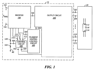
[0008] FIG. 1 is a partial block-diagram schematic of a ballast with lamp
filament detection,
in accordance with a preferred embodiment of the present invention;
-2-
CA 02729233 2010-12-23
WO 2009/158330 PCT/US2009/048236
[0009] FIG. 2 is a circuit diagram of a ballast for powering two lamps that
includes lamp
filament detection, in accordance with a preferred embodiment of the present
invention;
[0010] FIG. 3 is a circuit diagram of the ballast of FIG. 1, wherein the
ballast is utilized to
power only a single lamp, in accordance with a preferred embodiment of the
present invention;
[0011] FIG. 4a describes a voltage across a DC blocking capacitor as a
function of time in
the arrangements depicted in FIGS. 2 and 3 for a single lamp, in accordance
with a preferred
embodiment of the present invention; and
[0012] FIG. 4b describes a voltage across a DC blocking capacitor as a
function of time in
the arrangements depicted in FIGS. 2 and 3 for two lamps, in accordance with a
preferred
embodiment of the present invention.
Detailed Description of the Preferred Embodiments
[0013] FIG. 1 describes a ballast 10 for powering a gas discharge lamp load
20. Lamp load
20 includes at least one gas discharge lamp 30 having a pair of lamp filaments
32,34. Ballast 10
comprises an inverter 100, an output circuit 200, and a control circuit 500.
[0014] Ballast 10 preferably further includes a filament heating control
circuit 300 that is
coupled to output circuit 200 (via a first input 302), inverter 100 (via a
second input 304), and
control circuit 500 (via an input 504 of control circuit 500). A preferred
structure (as depicted in
FIGS. 2 and 3 herein) for realizing filament heating control circuit 300 is
described in further
detail in the aforementioned U.S. Patent Application titled "Ballast with Lamp-
Diagnostic
Filament Heating, and Method Therefor."
[0015] Referring again to FIG. 1, inverter 100 includes first and second input
terminals
102,104 and an inverter output terminal 106. First and second input terminals
102,104 are
adapted to receive a source of substantially direct current (DC) voltage,
VJjL, such as that which
is commonly provided by a combination of a full-wave rectifier (powered from a
conventional
AC source - e.g., 277 volts at 60 hertz) and a DC-to-DC converter circuit
(e.g., a boost
converter). VpJL is typically selected to have a steady-state operating
magnitude that is on the
order of several hundred volts; for example, for a commonly provided AC source
voltage of
-3-
CA 02729233 2010-12-23
WO 2009/158330 PCT/US2009/048236
277 volts rms, VRAIL is typically selected to have a steady-state operating
magnitude of about 450
volts. During operation, inverter 100 provides an alternating output voltage
(typically selected to
have a frequency in excess of 20,000 hertz) at inverter output terminal 106.
The operational
details of inverter 100 are known to those skilled in the art, and will not be
discussed in detail
herein. A preferred detailed structure for realizing inverter 100 is described
herein with
reference to FIGS. 2 and 3.
[0016] Output circuit 200 is coupled to inverter 100 and includes a plurality
of output
connections 202,204,...,210,212 adapted for coupling to one or more lamps
within lamp load 20.
During operation, output circuit 200 receives the alternating output voltage
at inverter output
terminal 106 and provides a high voltage for igniting, and a magnitude-limited
current for
operating, the lamp(s) within lamp load 20. Additionally, output circuit 200
serves, in
conjunction with filament heating control circuit 300, to provide appropriate
levels of excitation
for heating the filaments of the lamp(s) within lamp load 20. A preferred
structure for realizing
output circuit 200 is described herein with reference to FIGS. 2 and 3.
[0017] Control circuit 500 is coupled to inverter 100 and output circuit 200.
During
operation, and in a detection period (i.e., in the time between when power is
applied to ballast 10
and when inverter 100 begins to operate), control circuit 500 detects whether
or not one or more
lamps with intact lamp filaments are coupled to output connections
202,204,...,210,212. More
specifically: (1) in an arrangement wherein two lamps are coupled to the
output connections,
control circuit 500 detects whether or not both of the lamps have both
filaments intact; and (2) in
an arrangement wherein only a single lamp is coupled to the output
connections, control circuit
500 detects whether or not the single lamp has both filaments intact.
[0018] Thus, control circuit 500 operates to determine the presence of lamps
with intact
filaments that are connected to ballast 10. This determination may be utilized
in any of a number
of ways, such as for providing appropriate filament heating voltages, for
setting/adjusting
thresholds that are used for detecting lamp fault conditions, and/or for
accommodating
relamping.
-4-
CA 02729233 2010-12-23
WO 2009/158330 PCT/US2009/048236
[0019] As described in FIG. 1, control circuit 500 includes a filament
detection input 502
and a plurality of control outputs 510,511,512. Filament detection input 502
is coupled to output
circuit 200, while control outputs 510,511,512 are coupled to inverter 100.
[0020] During operation, in the detection period prior to startup of inverter
100, as well as
during a subsequent shutdown and/or monitoring mode, control circuit 500
receives, at filament
detection input 502, a voltage signal from output circuit 200 that indicates
whether or not one or
two lamps with intact lamp filaments are coupled to output connections
202,204,...,210,212.
Control circuit 500 provides a digital control signal at control outputs
510,511,512 in
dependence upon the voltage signal provided to filament detection input 502.
More specifically,
control circuit 500 provides a digital control signal at control output 512
which is then provided
to inverter 100 in dependence upon the voltage signal provided to filament
detection input 502.
Additionally, control circuit 500 provides digital control signals at control
outputs 510,511 which
are received by inverter 100 and which are utilized by inverter 100 to control
the timing of the
commutation of one or more electronic switches (e.g., power transistors)
within inverter 100
and heating control circuit 300.
[0021] In a preferred embodiment of ballast 10, as described in FIGS. 2 and 3,
control
circuit 500 is realized by a suitable programmable microcontroller, such as
the ST7LITEIB
microcontroller integrated circuit manufactured by ST Microelectronics. In the
following
description, control circuit 500 is hereinafter referred to as microcontroller
500.
[0022] FIGS. 2 and 3 describe a preferred detailed structure for ballast 10
that is suitable
for powering either two lamps (FIG. 2) or a single lamp (FIG. 3). It should be
appreciated that
microcontroller 500 is capable, provided that all filaments of the associated
lamp(s) are intact, of
distinguishing between the two-lamp arrangement of FIG. 2 and the one-lamp
arrangement of
FIG. 3. Consequently, the preferred embodiment of ballast 10 may be used to
power a lamp load
consisting of either two lamps or a single lamp. It should also be appreciated
that the principles
of the present invention are not limited to arrangements consisting of one or
two lamps, but may
be extended to arrangements that include three or more lamps.
-5-
CA 02729233 2010-12-23
WO 2009/158330 PCT/US2009/048236
[0023] Referring to FIG. 2, inverter 100 is preferably realized as a driven
half-bridge type
inverter comprising first and second inverter switches 110,120 (preferably
realized by N-channel
field-effect transistors, as depicted in FIG. 2) and an inverter driver
circuit 130. During
operation, inverter driver 130 receives (at inputs 140,141) logic-level (i.e.,
low voltage) control
signals from microcontroller 500 and, in response, commutates inverter
switches 110,120 (via
suitable drive signals provided at outputs 132,134,136) in a substantially
complementary fashion
(i.e., such that when transistor 110 is turned on, transistor 120 is turned
off, and vice-versa) and
at a high frequency rate that is typically selected to be greater than 20,000
hertz. Preferably, and
as will be appreciated by those skilled in the art, the control signals
provided at outputs 510,511
of microcontroller 500 (which control signals are received by inverter driver
circuit 130 via
inputs 140,141) dictate the timing of the commutation of FETs 110,120;
inverter driver circuit
130 effectively amplifies and level shifts those control signals so as to
provide appropriate drive
signals for turning FETs 110,120 on and off in a desired and efficient manner.
[0024] During operation of inverter 100, the output voltage that is provided
at inverter
output terminal 106 is a substantially squarewave voltage that, taken with
respect to circuit
ground 80, periodically varies between the magnitude of VJJL and zero.
Inverter driver circuit
130 may be realized by any of a number of suitable circuits or devices known
to those skilled in
the art, such as the L6382D5 integrated circuit manufactured by ST
Microelectronics.
Alternatively, inverter driver circuit 130 may be realized by any of a number
of discrete circuit
arrangements that are known to those skilled in the art.
[0025] As described in FIG. 2, inverter driver circuit 130 preferably includes
a plurality of
inputs 140,141,142 and a plurality of outputs 132,134,136,138. The signals at
inputs
140,141,142 and at outputs 132,134,136,138 are described as follows.
[0026] Input 140 of inverter driver circuit 130 is coupled to control output
510 of
microcontroller 500; the signal at input 140 is used to control the
commutation of inverter FET
110. More specifically, the logic-level (i.e., low voltage) signal provided at
output 510 of
microcontroller 500 is received at input 140 and is processed (i.e., amplified
and/or level-shifted)
by inverter driver circuit 130 so as to provide an output signal, between
outputs 132,134, having
-6-
CA 02729233 2010-12-23
WO 2009/158330 PCT/US2009/048236
a magnitude and power level that is sufficient for commutating FET 110 in a
desired and reliable
manner.
[0027] Along similar lines, input 141 of inverter driver circuit 130 is
coupled to control
output 511 of microcontroller 500; the signal at input 141 is used to control
the commutation of
inverter FET 120. More specifically, the logic-level (i.e., low voltage)
signal provided at output
511 of microcontroller 500 is received at input 141 and is processed (i.e.,
amplified and/or level-
shifted) by inverter driver circuit 130 so as to provide an output signal,
between output 136 and
circuit ground 80, having a magnitude and power level that is sufficient for
commutating FET
120 in a desired and reliable manner.
[0028] Referring again to FIG. 2, input 142 of inverter driver circuit 130 is
coupled to
output 512 of microcontroller 500 and output 510 of microcontroller 500 via
resistor 524. More
specifically, the logic-level (i.e., low voltage) signal provided at outputs
510 and 512 of
microcontroller 500 is received at input 142 and is processed (i.e., amplified
and/or level-shifted)
by inverter driver circuit 130 so as to provide an output signal, between
output 138 and circuit
ground 80, having a magnitude and power level that is sufficient for
commutating an electronic
switch (e.g., FET 310) within filament heating control circuit 300 in a
desired manner. Further
details concerning the operation of filament heating control circuit 300 are
disclosed in the
aforementioned U.S. Patent Application titled "Ballast with Lamp-Diagnostic
Filament Heating,
and Method Therefor."
[0029] In the preferred low-cost arrangement described with reference to FIG.
2, wherein
microcontroller 500 is preferably realized by a device such as the ST7LITEIB
integrated circuit
(manufactured by ST Microelectronics), a resistor 524 is coupled between
control outputs
510,512 of microcontroller 500. Resistor 524 is utilized so that the signal
(at output 512 of
micro controller 500) for controlling commutation of FET 310 (within filament
heating control
circuit 300) is substantially synchronized with the signal (provided at output
510 of micro-
controller 500) for controlling commutation of inverter FET 110. In this
preferred arrangement,
output 512 of microcontroller 500 is configured as a so-called "open drain
output" so as to allow
-7-
CA 02729233 2010-12-23
WO 2009/158330 PCT/US2009/048236
for deactivation of filament heating control circuit 300 (i.e., keeping FET
310 turned off) in
response to a digital signal.
[0030] As will be appreciated by those skilled in the art, the aforementioned
preferred
arrangement, wherein microcontroller 500 provides (at outputs 510,511,512)
logic-level signals
and inverter driver circuit 130 provides drive-level signals (i.e., signals,
at outputs 132,136,138,
having magnitudes and power levels that are sufficient for commutating power
transistors in a
desired manner), allows ballast 10 to be realized in a cost-effective manner.
The preferred
arrangement may be compared with a even more desirable alternative arrangement
wherein the
signal for commutating FET 310 is directly (as opposed to indirectly derived
from control signal
at output 510 of microcontroller 500) provided by microcontroller 500; such an
alternative
arrangement necessitates the incorporation of a more complex timer unit for
generating the 3
control signals 510,511,512 (e.g., pulse-width modulation generators) within
microcontroller
500, which is at the time of the invention not available in the market for a
reasonable cost
allowing for a low-cost solution.
[0031] Referring again to FIG. 2, output circuit 200 is preferably realized as
a series-
resonant type output circuit comprising first, second, third, fourth, fifth,
and sixth output
connections 202,204,206,208,210,212, a resonant inductor 220, a resonant
capacitor 224, a
direct current (DC) blocking capacitor CB, first and second voltage divider
resistors 260,262, a
plurality of resistances R1,R2,R3,R4, a capacitor 270, and filament heating
circuitry (comprising
secondary windings LFSi,LFS2,LFS3 and diodes 230,240,250). First and second
output
connections 202,204 are adapted for coupling to a first filament 32 of a first
lamp 30. Third and
fourth output connections 206,208 are adapted for coupling to a second
filament 34 of first lamp
30 and a first filament 42 of second lamp 40; as illustrated in FIG. 2, second
filament 34 of first
lamp 30 and first filament 42 of second lamp 40 are effectively connected in
series with each
other in a preferred embodiment, so third and fourth output connections
206,208 are adapted for
coupling to both filaments 34,42. Nonetheless other embodiments may use a
parallel connection
of second filament 34 of first lamp 30 and first filament 42 of second lamp
40. Fifth and sixth
output connections 210,212 are adapted for coupling to a second filament 44 of
second lamp 40.
Resonant inductor 220 is coupled between inverter output terminal 106 and a
first node 222.
-8-
CA 02729233 2010-12-23
WO 2009/158330 PCT/US2009/048236
Resonant capacitor 224 is coupled between first node 222 and circuit ground
80. DC blocking
capacitor CB is coupled between sixth output connection 212 and circuit ground
80. First voltage
divider resistor 260 is coupled between sixth output connection and voltage
detection input 502
of microcontroller 500. Second voltage divider resistor 262 is coupled between
voltage detection
input 502 of microcontroller 500 and circuit ground 80. First resistance RI is
coupled between
first input terminal 102 of inverter 100 and first output connection 202.
Second resistance R2 is
coupled between second output connection 204 and fifth output connection 210.
Third resistance
R3 is coupled between first input terminal 102 of inverter 100 and third
output connection 206.
Fourth resistance R4 and capacitor 270 are each coupled between fourth and
fifth output
connections 208,210.
[0032] Sequence start capacitor 270 coupled between output 208 and 210 in
parallel to
second lamp 40 will act as a capacitive voltage divider together with lamp
leakage capacities and
leakage capacitance of lamp wiring. This voltage divider is effecting the lamp
voltages prior to
striking of both lamps. Lamp voltage of lamp 30 will be much higher than lamp
voltage of lamp
40 until lamp 30 strikes. After strike of lamp 30 nearly all output voltage of
resonant output
circuit 200 will be applied to lamp 40 and strike this lamp after lamp 30 in a
sequential order.
[0033] Resistances R1,R2,R3,R4 (each of which may be realized by one or more
resistors,
as dictated by practical design considerations such as voltage and power
ratings) collectively
serve to allow microcontroller 500 to determine whether or not intact lamp
filaments are
connected to output connections 202,204,206,208,210,212. More particularly, in
a detection
period that occurs prior to startup of inverter 100 (i.e., before inverter 100
begins to operate and
provide commutation of inverter switches 110,120), resistances R1,R2,R3,R4 (in
conjunction
with filaments 32,34,42,44 of lamps 30,40) provide filament current paths
through which DC
currents flow, provided that the associated lamp filaments are intact, into DC
blocking capacitor
CB. In the two-lamp arrangement illustrated in FIG. 2, there are two distinct
filament current
paths; a first filament current path involves first filament 32 of first lamp
30 and second filament
44 of second lamp 40, and a second filament current path involves second
filament 34 of first
lamp 30, first filament 42 of second lamp 40, and second filament 44 of second
lamp 40. In the
-9-
CA 02729233 2010-12-23
WO 2009/158330 PCT/US2009/048236
one-lamp arrangement illustrated in FIG. 3, there is a single filament current
path that involves
first and second filaments 32,34 of lamp 30.
[0034] The filament heating circuitry within output circuit 200 comprises a
plurality of
series combinations including secondary windings LFSI,LFS2,LFS3 and diodes
230,240,250.
A series combination of secondary winding LFSZ and diode 230 is coupled
between first node 222
(which also connects to output 202) and second output connection 204; diode
230 has an anode
232 coupled to second output connection 204 and a cathode 234 coupled to LFS1
thus blocking
the DC path between output 202 and output 204 (except directly through the
filaments as will be
understood by those skilled in the art). The order of diodes and secondary
windings within the
series combination is determined by printed circuit board design
considerations and may be
swapped in other implementations. A series combination of secondary winding
LFS2 and diode
240 is coupled between third and fourth output connections 206,208; diode 240
has an anode 242
coupled to fourth output connection 208 and a cathode 244 coupled to LFS2 thus
blocking DC
path between output 206 and 208. A series combination of secondary winding
LFS3 and diode
250 is coupled between fifth and sixth output connections 210,212; diode 250
has an anode 252
coupled to LFS3 and a cathode 254 coupled to fifth output connection 210 thus
blocking the DC
path between output 210 and output 212. Secondary windings LFSI,LFS2,LFS3 are
each
magnetically coupled to a primary winding LFP within filament heating control
circuit 300.
During operation, secondary windings LFSI,LFS2,LFS3 provide heating of lamp
filaments
32,34,42,44, and diodes 230,240,250 serve to effectively isolate
LFSI,LFS2,LFS3 from the filament
current paths provided by resistances R1,R2,R3,R4.
[0035] Further details concerning the preferred operation of secondary
windings
LFSI,LFS2,LFS3 and filament heating control circuit 300 are provided in the
aforementioned U.S.
Patent Application titled "Ballast with Lamp-Diagnostic Filament Heating, and
Method
Therefor."
[0036] Resistances RI and R2 together serve to provide the first filament
current path that
includes first filament 32 of first lamp 30 and second filament 44 of second
lamp 40. That is,
during operation of ballast 10 and in the period prior to startup of inverter
100, if filaments 32
-10-
CA 02729233 2010-12-23
WO 2009/158330 PCT/US2009/048236
and 44 are both intact, a first DC current flows from first inverter input
terminal 102, through
resistance RI, out of output connection 202, through filament 32, into output
connection 204,
through resistance R2, out of output connection 210, through filament 44, into
output connection
212, through the parallel combination of capacitor CB and voltage divider
resistors 260,262, and
into circuit ground 80. The first DC current, taken by itself, contributes a
voltage equal to
Ki *VRAIL (where Ki is a constant that is determined by the voltage divider
formed by the
resistances R1,R2 and resistors 260,262, the filament resistances within the
current path are
several magnitudes smaller than the other resistances and can therefore be
neglected in
calculating the constant K1) to the voltage, VB, that appears across DC
blocking capacitor CB
prior to startup of inverter 100.
[0037] Resistances R3 and R4 together serve to provide the second filament
current path
that includes second filament 34 of first lamp 30, first filament 42 of second
lamp 40, and second
filament 44 of second lamp 40. That is, during operation of ballast 10 and in
the period prior to
startup of inverter 100, if filaments 34, 42, and 44 are all intact, a second
DC current flows from
first inverter input terminal 102, through resistance R3, out of output
connection 206, through
filament 34, through filament 42, into output connection 208, through
resistance R4, out of
output connection 210, through filament 44, into output connection 212,
through the parallel
combination of capacitor CB and voltage divider resistors 260,262, and into
circuit ground 80.
The second DC current, taken by itself, contributes a voltage equal to
K2*VRAIL (where K2 is a
constant that is determined by the voltage divider formed by the resistances
R3,R4 and resistors
260,262, and that is preferably chosen to be less than the constant Ki
associated with the first
filament current path) to the voltage, VB, that appears across DC blocking
capacitor CB prior to
startup of inverter 100. It should be appreciated that both the first and
second filament current
paths include second filament 44 of lamp 40 in this embodiment thereby
providing safer
conditions of operation.
[0038] When both the first and second filament current paths are intact (i.e.,
when filaments
32,34,42,44 are all intact), the voltage VB that appears across DC blocking
capacitor CB prior to
startup of inverter 100 is equal to K3*VRAJL (where K3 is a constant that is
determined by the
-11-
CA 02729233 2010-12-23
WO 2009/158330 PCT/US2009/048236
voltage divider formed by the resistances RI, R2, R3, R4 and resistors 260,
262). K3 is therefore
greater than constants Ki and K2 as a person skilled in the art would
understand.
[0039] Voltage detection input 502 of microcontroller 500 is coupled to DC
blocking
capacitor CB via voltage divider resistors 260,262. More specifically, voltage
detection input
502 is coupled to a junction of first voltage divider resistor 260 and second
voltage divider
resistor 262, and the series combination of first voltage divider resistor 260
and second voltage
divider resistor 262 is coupled in parallel with capacitor CB (i.e., between
sixth output connection
212 and circuit ground 80). It should be understood that the voltage Vx across
resistor 262 is
simply a scaled-down version of the voltage VB across DC blocking capacitor
CB.
[0040] In a preferred embodiment of ballast 10, microcontroller 500 provides a
first timing
function (hereinafter referred to in connection with "the first timer") and a
second timing
function (hereinafter referred to in connection with "the second timer").
First timer and second
timer are used by the microcontroller firmware to filter the measured voltage
Vx until one or
both timers will overflow, thus incorporating digital filters to minimize
noise influence on signal
Vx. The time constants of the filter, which are basically the timer overflow
thresholds multiplied
with the sample time interval of signal VX, are chosen higher than the time
constant of the
network formed by DC blocking cap CB and filament detection resistors R1,R2
and resistors 260
and 262. Microcontroller 500 utilizes the first and second timing functions to
provide the
following logic with respect to the voltage signal, Vx, received at voltage
detection input 502
during the detection period.
1. If VB exceeds a first predetermined threshold, VTH1 (corresponding to
Ki*VpJL
> VTHi > K2*VpJL), but does not exceed a second predetermined threshold, VTH2
(corresponding to K3 * VRAIL > VTH2 > Ki * VRAIL), the first timer is started
and is
periodically incremented at each sample time interval of voltage VX until such
time as either: (i) VB exceeds VTH2; or (ii) the first timer reaches a
predetermined
overflow limit (i.e., which means that VB has remained between VTH1 and VTH2
for a predetermined period of time, thereby indicating that only a single lamp
with
both filaments intact is coupled to the output connections).
-12-
CA 02729233 2010-12-23
WO 2009/158330 PCT/US2009/048236
2. If VB exceeds VTH2 (corresponding to K3*VpJL > VTH2 > Ki*VpJL, indicating
that both the first and second filament paths are intact), the first timer is
stopped,
a second timer is started, and the second timer is periodically incremented at
each
sample time interval of voltage VX until such time as it reaches the
predetermined
overflow limit (i.e., which means that VB has remained above VTH2 for a
predetermined period of time, thereby indicating that two or more lamps with
all
filaments intact are coupled to the output connections).
3. If VB does not exceed a first predetermined threshold, VTHZ, indicating
that no
filament path is intact, first and second timer are periodically decremented
to zero
at each sample time interval of voltage V.
[0041] If the first timer reaches the predetermined overflow limit (which
indicates the
presence of a single lamp with both filaments intact, as in the arrangement
described in FIG. 3),
microcontroller 500 will enter preheat mode and select a prestored parameter
set from internal
memory suitable for driving inverter 100 and heating circuit 300 in a single
lamp mode. If the
second timer reaches the predetermined overflow limit (which indicates the
presence of two
lamps with both filaments of each lamp being intact, as in the arrangement
described in FIG. 2),
microcontroller 500 will enter preheat mode and select a prestored parameter
set from internal
memory suitable for driving inverter 100 and heating circuit 300 in a two lamp
mode. If neither
the first timer nor the second timer reaches the predetermined overflow limit
(which indicates the
presence of no lamps with both filaments intact), microcontroller 500 will not
start the inverter
100 and heating circuit 300 (control signals 140, 141 and 142 remain at logic
level of zero) and
remain in a filament detection and monitoring mode (e.g., waiting for lamps to
be inserted or
replaced). The signal provided by inverter driver circuit 130 at auxiliary
output 138 is used to
control the filament heating provided by filament heating control circuit 300
and the filament
heating circuitry (i.e., LFSI,LFS2,LFS3 and diodes 230,240,250) within output
circuit 200; an
example of this is described in further detail in the aforementioned U.S.
Patent Application titled
"Ballast with Lamp-Diagnostic Filament Heating, and Method Therefor."
-13-
CA 02729233 2010-12-23
WO 2009/158330 PCT/US2009/048236
[0042] It should be appreciated that a condition in which VB = K2*VpJL (i.e.,
which occurs
when only the second filament current path, including R3 and R4, is intact) is
essentially ignored
by microcontroller 500, and is treated in the same manner as a condition
wherein no lamps with
intact filaments are present. To ensure this functionality, it is important,
as previously
mentioned, that K2 be chosen to be less than K1.
[0043] Microcontroller 500 preferably includes an input 506 for monitoring the
DC rail
voltage, VRAIL, as well as a current-sensing input 504 for monitoring the
current that flows in
filament heating control circuit 300. The provision of input 506 is useful in
that it allows
microcontroller 500 to effectively "track" the magnitude of VP JL; this
capability is desirable
because the filament detection function of microcontroller 500 is dependent
upon the magnitude
of VJJL, yet the magnitude of VRAIL is subject to certain variations during
operation (due to, for
example, a brown-out condition or an overvoltage condition at the AC power
source). The
functionality associated with current-sensing input 504 is discussed in
further detail in the
aforementioned U.S. Patent Application titled "Ballast with Lamp-Diagnostic
Filament Heating,
and Method Therefor."
[0044] Preferably, filament heating control circuit 300 comprises a first
input 302, a second
input 304, an electronic switch 310, a primary filament heating winding LFP, a
current-sensing
resistor 318, a capacitor 320, and a diode 330. Electronic switch 310 is
preferably realized as an
N-channel field effect transistor (FET) having a gate 312, a drain 316, and a
source 314. Gate
312 is coupled to second input 304. Capacitor 320 is coupled between first
input 302 and a node
324. Diode 330 has an anode 332 coupled to first input 302 and a cathode 334
coupled to node
324. Primary filament heating winding LFP is coupled between node 324 and
drain 316 of FET
310. Current-sensing resistor 318 is coupled between source 314 and circuit
ground 80.
[0045] Preferably, as described in FIG. 2, filament heating control circuit
300 also includes
a voltage clamping diode 340 having an anode 342 coupled to drain 316 (of FET
310) and a
cathode 344 coupled to input terminal 102 of inverter 100.
[0046] Secondary filament heating windings LFS1, LFS2, and LFS3 (located
within output
circuit 200) are magnetically coupled to primary filament heating winding LFP,
and provide
-14-
CA 02729233 2010-12-23
WO 2009/158330 PCT/US2009/048236
filament heating voltages which are controlled by filament heating circuit
300. Within output
circuit 200, diodes 230,240,250 are present in order to electrically isolate
filament heating
windings LFSI,LFS2,LFS3 from the DC current paths (involving R1,R2,R3,R4 and
the filaments
32,34,42,44 of lamps 30,40) that are used to ascertain the number of lamps
with intact filaments
that are coupled to the output connections of ballast 10.
[0047] A more detailed description of the operation of filament heating
control circuit 300 is
provided in the aforementioned U.S. Patent Application titled "Ballast with
Lamp-Diagnostic
Filament Heating, and Method Therefor."
[0048] The operation of ballast 10 is now described with reference to FIG. 2
as follows.
[0049] When both lamps 30,40 are present with both filaments of each lamp
being intact,
both the first and second filament current paths are intact; accordingly, both
the first and second
DC currents flow into the parallel circuit that includes DC blocking capacitor
CB and voltage
divider resistors 260,262. Consequently, the voltage VB (as defined and
characterized above)
across DC blocking capacitor CB will be at a first (i.e., relatively high)
level; when only one lamp
(with both filaments intact) is present, VB will be at a second (i.e.,
relatively low) level. Thus,
the magnitude of VB prior to startup of the inverter is indicative of the
number of functional
lamps (i.e., lamps with intact filaments) that are connected to the output of
ballast 10.
Correspondingly, a scaled-down version of VB -- i.e., Vx -- is conveyed to
microcontroller 500.
Vx is interpreted by microcontroller 500 to determine whether or not lamps
with intact filaments
are present.
[0050] As described in FIG. 2, preferably, the resulting control signals (from
outputs 510,
511 and 512 of microcontroller 500) are received by inverter driver circuit
130 (via inputs 140,
141 and 142) and are used to provide appropriate drive signals (via outputs
132,134,136 and
138) to inverter FETs 110 and 120 and to filament heating control circuit 300.
[0051] A graphical description of the previously described functionality is
provided in
FIG. 4a for 1 lamp operation and FIG. 4b for 2 lamp operation, which
illustrates approximate
-15-
CA 02729233 2010-12-23
WO 2009/158330 PCT/US2009/048236
waveforms for VB, VJJL and timer values. VTH1 and VTH2 in FIG. 4a and FIG. 4b
are to be
understood as being proportional to Vxi and Vx2, respectively.
[0052] Referring to FIG. 4a, AC power is initially applied to ballast 10 at
time ti. The DC
rail voltage, VpJL, does not reach its steady-state operating value (e.g.,
about 450 volts) until
power factor correction circuit and inverter 100 are started at time t3. Prior
to time t3, VpJL is
at the peak of the AC line voltage (e.g., about 390 volts, for an AC power
source voltage of
277 volts rms). Between time ti and time t3, the voltage across DC blocking
capacitor CB ramps
up and eventually levels out. Until time t3, which represents either first or
second timer is
reaching the predetermined overflow limit, microcontroller 500 is actively
monitoring Vx
(which, as previously explained, is simply a scaled-down version of VB). At
time t2 VB is
crossing VTH1 and the first timer is starting to be increased periodically. At
time t3, which
signifies the beginning of the preheat phase, VRAIL transitions to its steady-
state operating
value (e.g., 450 volts) and microcontroller 500 starts to apply control
signals to inverter 100
and filament control circuit 300 to provide preheating of the lamp filaments.
At time t4, the
preheating phase is completed and an ignition voltage is applied for starting
the lamps. Once
the lamps ignite, the voltage VB across DC blocking capacitor CB transitions
to a steady-state
operating value that is approximately equal to one half of VpJL (e.g., about
225 volts, when
VpJL is set at 450 volts). Subsequently (i.e., in the "operating phase" which
occurs after time
t4), ballast 10 supplies operating power to the lamps. Control signal 512 of
micro controller 500
is set to zero in operation mode to turn off filament heating in the preferred
low cost embodi-
ment. However, other embodiments of the invention may use an independent PWM
generator to
control the dutycycle of the logic level signal on output 512 of
microcontroller 500 independent
of the dutycycle of logic level signal 510 of microcontroller 500, thus
allowing change to the
heating of heating circuit 300 during normal operation to any desired level.
[0053] In FIG. 4b, the trace that is labeled "VB (2 lamps)" depicts the
voltage, VB, across
DC blocking capacitor CB in the two-lamp arrangement described in FIG. 2 under
a condition
wherein all of the filaments 32,34,42,44 of lamps 30,40 are intact. The trace
that is labeled
"VB (1 lamp)" depicts the voltage, VB, across DC blocking capacitor CB in the
one-lamp
-16-
CA 02729233 2010-12-23
WO 2009/158330 PCT/US2009/048236
arrangement described in FIG. 3 under a condition wherein both of the
filaments 32,34 of lamp
30 are intact.
[0054] It should be appreciated that the trace labeled "VB (1 lamp)" in FIG.
4a is also
representative of the voltage, VB, across DC blocking capacitor CB that occurs
in the two-lamp
arrangement described in FIG. 2 under a condition wherein: (i) one or both of
filaments 34,42
are not intact (i.e., the second filament current path, which includes R3 and
R4, is open); and
(ii) filaments 32,44 are both intact. However, as explained in further detail
herein, this condition
is treated as a lamp fault condition by associated protection circuitry within
ballast 10, and is
therefore of no consequence to the intended operation of microcontroller 500.
[0055] It should also be understood that there is a third possibility for VB
that is not depicted
in FIG. 4a or FIG. 4b. More particularly, in the two-lamp arrangement
described in FIG. 2, and
under a condition wherein filament 32 is open but the remaining filaments
34,42,44 are intact
(i.e., the first filament path, including RI and R2, is open, but the second
filament path, including
R3 and R4, is intact), VB will reach a magnitude that is less than VTH1. As
discussed in further
detail herein, that condition is essentially ignored by microcontroller 500,
and is effectively
treated as a condition wherein no lamps with both filament intact are present
(even though, in
fact, both filaments 42,44 of lamp 40 may be intact).
[0056] The operation of ballast 10 in the two-lamp arrangement of FIG. 2 under
various
conditions (i.e., with respect to whether or not certain lamp filaments are
intact) is described as
follows.
[0057] Under a condition wherein filaments 32,34,42,44 of lamps 30,40 are all
intact, both
the first and second filament current paths are intact. Consequently, VB will
equal K3*VRAIL, and
will therefore exceed VTH2 for at least most of the duration of the detection
window between t2
and t3. In that case, by time t3, the second timer within microcontroller 500
will have reached
its predetermined overflow limit, thereby causing microcontroller 500 to
select a prestored
parameter set from the internal memory for configuring the inverter regulator
firmware
algorithms and the fault detection firmware algorithms that is representative
of the fact that two
lamps, each having both filaments intact, are coupled to the output
connections of ballast 10.
-17-
CA 02729233 2010-12-23
WO 2009/158330 PCT/US2009/048236
[0058] Under a condition wherein filament 44 is open, and regardless of
whether or not
filaments 32,34,42 are intact, neither the first nor the second filament
current paths, both of
which include filament 44, are intact. Consequently, VB will remain at zero
until lamp 40 is
inserted or replaced with a new lamp with intact filament 44. In that case
neither of the timers
within microcontroller 500 will start counting and reach the predetermined
overflow limit,
thereby causing microcontroller 500 to select a parameter set so that the
inverter does not enter
preheat mode. As previously mentioned, safety concerns dictate that a
condition in which
filament 44 is open should be treated in a special manner, even when both
filaments 32,34 of
lamp 30 are intact.
[0059] Under a condition wherein either one of filaments 34,42 is open, and
irrespective
of whether the remaining filaments 32,44 are intact, the second filament
current path (which
includes R3 and R4) is open (i.e., not intact). Consequently, VB will be
limited, prior to inverter
startup, to a value that is no greater than Ki*VRAIL. Under these conditions,
VB will reach
Ki*VRAIL during the detection period only if filaments 32,44 are both intact,
in which case VB
will exceed VTH1, but not VTH2. From the point of view of microcontroller 500,
this condition
will appear to be the same as the one-lamp arrangement (with both filaments of
the single lamp
being intact) depicted in FIG. 3. However, with the second filament current
path being open,
neither of the two lamps 30,40 will receive heating of their associated
filaments 32,44, and will
therefore not ignite and/or operate in a normal manner; that being the case,
lamp heating circuitry
300 within ballast 10 will be configured and controlled by firmware of
microcontroller 500 as if
only one lamp with functional filaments would be present.
[0060] To summarize, in the two-lamp arrangement described in FIG. 2, the
parameter set
selected by microcontroller 500 to control inverter 100, heating circuit 300
and to configure fault
detection circuitry may assume one of several different values, depending upon
the conditions
(i.e., intact or open) of lamp filaments 32,34,42,44. More specifically, the
generation of the
control signals 510,511,512 is configured at: (i) a first value-array (e.g.,
on-time 1, deadtime 1,
frequency 1, fault condition thresholds 1) in response to a condition wherein
timer 1 is
overflowing; (ii) a second value-array (e.g., on-time 2, deadtime 2, frequency
2, fault condition
thresholds 2)in response to a condition wherein second timer is overflowing;
-18-
CA 02729233 2010-12-23
WO 2009/158330 PCT/US2009/048236
[0061] FIG. 3 describes an alternative application in which ballast 10 is
utilized to power a
single lamp 30. First and second output connections 202,204 are adapted for
coupling to a first
filament 32 of lamp 30. Fifth and sixth output connections 210,212 are adapted
for coupling to
a second filament 34 of lamp 30. In the one-lamp arrangement of FIG. 3, third
and fourth output
connections 206,208 are not utilized, and there is only a single filament
current path (which
includes R1 and R2). Consequently, resistances R3 and R4 serve no meaningful
function in the
operation of ballast 10 in the one-lamp arrangement depicted in FIG. 3.
[0062] The operation of ballast 10 in the one-lamp arrangement of FIG. 3 under
various
conditions (i.e., with respect to whether or not certain lamp filaments are
intact) is described as
follows.
[0063] Under a condition wherein both filaments 32,34 are intact, the single
filament current
path is intact. Consequently, VB will exceed VTH1 but will remain below VTH2
because the
second filament current path (i.e., including R3 and R4) is open. In that
case, by time t3, the first
timer within microcontroller 500 will have reached its predetermined overflow
limit, thereby
causing microcontroller 500 to select a prestored parameter set from the
internal memory for
configuring the inverter regulator firmware algorithms and the fault detection
firmware
algorithms that is representative of the fact that both filaments 32,34 of the
single lamp 30 are
intact.
[0064] Under a condition wherein either one or both of filaments 32,34 are not
intact, the
single filament current path will be open. Consequently, VB will be at zero,
and microcontroller
500 will interpret that as signifying that no lamp with both filaments intact
is present.
[0065] To summarize, in the one-lamp arrangement described in FIG. 3, the
generation of
the control signals 510,511,512 is configured at the first value-array (e.g.,
on-time 1, deadtime 1,
frequency 1, fault condition thresholds 1) in response to a condition wherein
timer 1 is
overflowing.
[0066] In this way, ballast 10 operates in arrangements including a single
lamp or multiple
lamps to detect the presence of lamps with intact filaments. As previously
described, this
-19-
CA 02729233 2010-12-23
WO 2009/158330 PCT/US2009/048236
detection may be used for any of a number of useful purposes, such as for
providing appropriate
levels of filament heating and/or for setting thresholds used in detecting
lamp fault conditions.
[0067] Although the present invention has been described with reference to
certain preferred
embodiments, numerous modifications and variations can be made by those
skilled in the art
without departing from the novel spirit and scope of this invention. For
example, although the
preferred embodiments described herein have specifically described
arrangements involving two
lamps and a single lamp, it should be appreciated that the principles of the
present invention may
be readily adapted and applied to ballasts for powering three or more lamps.
As another
example, a separate driver circuit for FET 310 could be employed instead of
sharing the one
driver circuit for the three FETs denoted by reference numerals 110, 120, and
310. As another
example a more sophisticated microcontroller 500 with additional PWM modules
could be used
to control the dutycycle of inverter input 142 independent of inverter input
140 thus allowing for
heating filaments of lamps 30 and 32 also during regular operation at any
desired level rather
than having only on/off capability for control during normal operation mode.
-20-